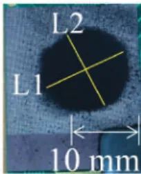
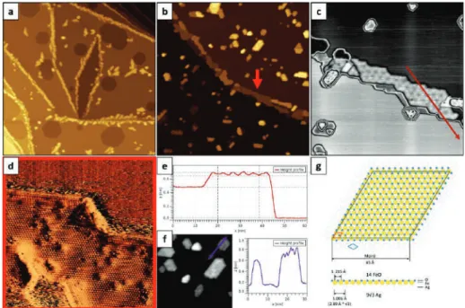
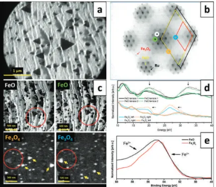
An atomic-resolution image of such an island shown in Fig. 1d revealed a close-packed atomic arrangement with a periodicity of ~3.2 Å, while its line profile presented in Fig. 1e provided information about the height of a typical Moiré-reconstructed island (~2.1 Å), Moiréperiod. The slope of the curve obtained for the islands without reconstruction on the HT-FeO/Ag(111) sample was much higher than that of pure Ag(111) and lower than that of Pt(111).
Conclusions
Efficient iterative schemes for ab initio total-energy calculations using a plane-wave basis set. Phys. Photoelectron spectroscopy study of the electronic structure of Au and Ag overlays on Pt(100), Pt(111), and Pt(997) surfaces. Phys.
Introduction
The results provided information on the growth, structure, electronic and magnetic properties of the films at the nanometer scale. In addition to the well-known dependence of the film morphology on the growth conditions, the results reveal the influence of the substrates' symmetry - more precisely: the mutual orientation of adjacent substrate monatomic terraces - on the structure of iron oxide islands and films epitaxially grown on top of them.
Materials and Methods
However, none of these studies comprehensively addressed the influence of the symmetry of different substrates on the structure of iron oxide islands and films grown on top of them. This work reports a comparative LEEM/XPEEM and μLEED surface science study of the growth and structure of FeO and Fe3O4 films on Pt(111) and Ru(0001).
Results and Discussion
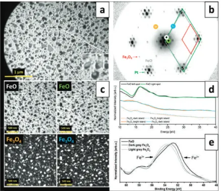
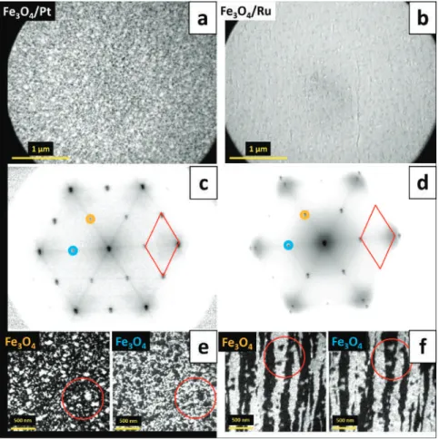
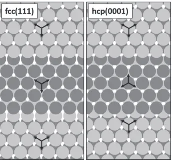
However, in our case, dark-field imaging of two neighboring Fe3O4(111) diffraction spots (i.e., (2×2) dots relative to Pt dots) did not result in two different image contrasts, thus indicating that all Fe3O4 islands have the same in-plane orientation (Figure 2c). Such a growth mode can be explained by the adaptation of symmetric triple iron oxides to the terraces of the triple symmetric substrate and leads to the natural structuring of iron oxide films, i.e., the formation of patch-like magnetite layers on Pt(111) and Fe3O400 and strip-like structures on Fe3O4001).
Self-Catalyzed CdTe Wires
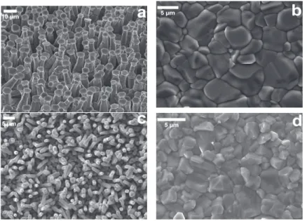
These substrates were especially chosen to separate the influence of the deposition surface from the surface roughness. Figure 5a,b shows SEM images of wire and planar layers grown by vacuum on SLG/Mo and SLG/FTO/Mo, respectively, with corresponding CL images shown in Figure 5c,d.
Scalable Fabrication of High-Performance Transparent Conductors Using Graphene
Results
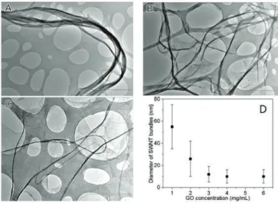
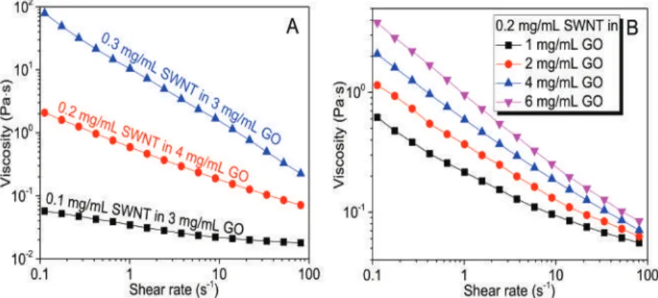
We prepared a series of GO-SWNT dispersions with different mass ratios of GO to SWNTs and found that homogeneous dispersions can only be obtained when the mass ratio reaches at least 5, at a concentration of 0.2 mg/mL SWNTs. The zeta potential measurements on these GO-SWNT dispersions are in reasonable agreement with the absorption spectra findings. For the GO-SWNT dispersion with a high SWNT content (0.02 mg/mL), the zeta potential remains almost unchanged.
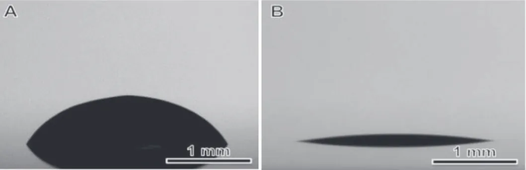
The relatively larger contact angle indicated a relatively poor wetting of the GO-SWNT ink on PET. For GO-SWNT dispersions, this behavior originates from debundling of nanotubes and/or from the increased orientation of nanotubes in the flow direction. As shown in Figure 6 , the resulting rGO-SWNT film contained a small amount of oxygen, compared to GO-SWNT film, indicating that the microwave treatment is very effective in removing the oxygen groups.
It can be seen that the films produced by the GO-SWNT system outperform other systems in terms of electro-optical properties. Due to the increased nonpolar nature of rGO compared to GO sheets, the rGO–SWNT interactions should be much stronger than the GO–SWNT interactions.
Optical Study and Experimental Realization of Nanostructured Back Reflectors with Reduced
Experimental Details
The overall fabrication process and SEM image of the hexagonal rear reflector is shown in Figure 1. Figure 3 shows reflectance data from sputtered ZnO (0 to 160 nm) on 200 nm sputtered Ag on the glass. This calculation matches the observation of the red shift of the reflectance minima with increasing ZnO thickness.
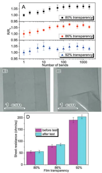
With the above understanding of flat Ag/ZnO BRs performance, the reflection results of ASAHI BRs are presented in the next section. The diffuse reflectance is an indirect way to characterize the scattering ability of the BRs [25]. Total and diffuse reflection of hexagonal Ag/ZnO nanostructured back reflectors Figure 6a,b shows the total and diffuse reflection of the hexagonal nanostructured BRs and ASAHI BR with 100 nm ZnO (see Figure 5 for SEM images).
To validate our simulation results, simulated overall absorption and measured absorption (1-measured reflectance) of the flat Ag/ZnO BR solar cell device are plotted in Figure 9b. Nanostructured back reflectors fabricated using polystyrene supported lithography for improved light trapping in silicon thin film solar cells.Sol.

Influence of InAlN Nanospiral Structures on the Behavior of Reflected Light Polarization
The optical properties of the resulting nanospirals were analyzed by Mueller matrix spectroscopic ellipsometry (MMSE) and the CompleteEASE software [21,22]. The main Pcpeak wavelength and band of reflected light were found to be highly correlated with the pitch, length, twist and composition of the grown InAlN nanospirals. The mirror shape of the two curves is evidence of high reproducibility in the MSE growth process.
SEM images of (a) right-handed and (b) left-handed indium aluminum nitride (InAlN) nanocoil film; (c) X-ray diffraction (XRD) patterns of right- and left-handed nanospirals; (d) Pc versus wavelength of the light reflected from nanospirals of opposite handedness. In addition, the thickness of the film-like nanostructure is thinner than that of the well-separated nanospirals. In this section we have the effect of the TiN seed layer thickness on |Pc| studied and the associated peak wavelength.
Therefore, precise control of the pitch of the grown nanospirals is important for the design of chiral optical response elements. The degree of circular polarization of the reflected light and the corresponding wavelength range were found to be highly dependent on the buffer thickness, pitch and morphology of nanospirals.

Linear Birefringent Films of Cellulose Nanocrystals Produced by Dip-Coating
The transmission (T) spectra at normal incidence of unpolarized light from the cellulose side of the dip-coated CNC films are shown in Figure 2. Figure 4 shows polar contour maps of the normalized Mueller matrix transfer data of dip-coated CNC films. To quantitatively determine the polarization properties of the dip-coated CNC films, we used differential (logarithmic) decomposition of the measured Mueller matrices.
The fact that CD and CBare zero indicates the absence of chiral phase in the films. The lack of chiral phase in the films is attributed to the short drying time. Figure A1 shows the X-ray diffraction data of the filter paper used as the cellulose source and of the dip-coated CNC films at draw speeds of 10 and 20 cm/min.
Figure A2 shows the FTIR spectra of filter paper, which was used as the cellulose source, and dip-coated CNC films at pullout speeds of 10 and 20 cm/min. The SEM images used to determine the thickness of the dip-coated CNC films at pullout speeds of 10 and 20 cm/min are shown in Figure A3.

Interfacial Model and Characterization for Nanoscale ReB 2 /TaN Multilayers at Desired Modulation Period
Results and Discussion 1. Microstructure Characterizations
HReB2/TaN=HReB2tReB2/Λ+HTaNtTaN/Λ (2) The calculated rule-of-mix hardness of the ReB2/TaN multilayer atΛ= 10 nm entReB2:ttaN. Detailed analyzes of the deformation mechanisms and the interface model will be presented in Section 3.3. Almost all the multilayers exhibit lower residual stress than the average value of the monolithic ReB2 and TaN coatings.
Figure 5a-d shows the results of the scratch test at differenttZrB2:tAlNandΛ, which reflects the fracture resistance of the ReB2/TaN multilayers. When considering the ideal growth of the ReB2 and TaN layers, B-terminated surfaces of ReB2(001) and Ta-terminated surfaces of TaN(111) are built in the ReB2(001)/TaN(111) configuration for the B-Ta. It is worth noting that the interfacial energy at differenttReB2:tTaN follows the similar trend as that of the residual stress.
The difference for this work from the reference report [44] in the modulation ratio of the most stable interface is due to the difference in the lattice structure and interfacial bonding for different elements in the interface. The multilayers at 1:3 atReB2:tTaN show the lowest residual stress, which corresponds to the lowest interfacial energy and the highest adsorption energy of the 9ReB2/21TaN interfacial structure.

Metal (Ag/Ti)-Containing Hydrogenated Amorphous Carbon Nanocomposite Films with Enhanced
Nanoscratch Resistance: Hybrid PECVD/PVD System and Microstructural Characteristics
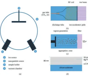
Nanocomposite films of a–C:H:Ag and a–C:H:Ti were deposited by sequential operation of the PECVD and PVD guns. Prior to the deposition of the nanocomposite films, a series of pristine a-C:H films were deposited to study the effects of ion source characteristics on the deposition rate and physical properties of the films. Figure 2b quantifies the effect of argon gas flow on the deposition rate of the a–C:H films.
In order to quantify the sizes of Ag and Ti NPs, the images were digitally analyzed. The details of the nanocomposite films prepared and tested in this study are shown in Table 3. The deposition details of the nanocomposite films grown in this study and the resulting surface roughness quantified by AFM.
This is related to the graphitization of the matrix with the introduction of metallic NPs and the release of energy trapped in angular and linear bond distortions. The structure of the silver-containing diamond-like carbon films: Investigation by multiwavelength Raman spectroscopy and XRD.Diam.
Enhancing the Microparticle Deposition Stability and Homogeneity on Planer for Synthesis
Experimental and Simulation Setup
The simulation shows that the flow velocity distribution of the 60mm cap was more even than that of the 20mm cap. The flow direction of the 60mm cap was also more constant than that of the 20mm cap. This result supports the simulation result that the 60 mm nozzle can stabilize the airflow and thus the deposition.
Since the mesh can stabilize the microparticle deposition, the effects of mesh size, pressure, and flow rate on microparticle deposition with the mesh were investigated to further improve the deposition stability. The airflow through the mask generated less and less turbulence between the mask and the substrate. Therefore, we investigated pressure and flow rate effects on deposition with a 3 mm orifice (Figure 9) and also compared the results with deposition without meshes (Figure 5).
Increasing the pressure and flow rate generated turbulence and eddy, resulting in instability in. With a 6 mm orifice, lowering the pressure or decreasing the flow rate increased deposit stability.