SAC solder joint for current load of 100 hours at an electromigration temperature of 100oC at thermal aging duration of (a) 0 hours and (b) 480 hours .. 65 Figure 4.15 SEM images of the microstructure of SAC solder materials a) SAC105 and b) . 89 Figure 5.5 Variation of the maximum value of PLWK at current density of 1.11× 10⁸A/m2 at a thermal aging temperature of 100oC and test temperature of 100oC for different thermal aging durations with and without applied random vibration.
- Moore’s Law
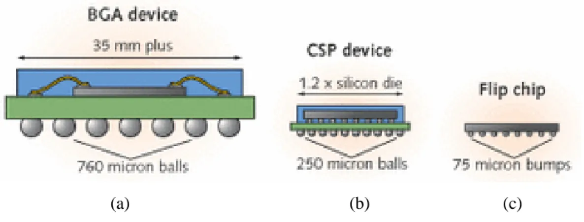
- Package Type Definitions
- Different Failure Modes of Solder Joint
- Electromigration
- Mechanism of Electromigration
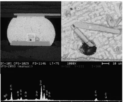
- Intermetallic Compound (IMC)
The diffusion of the atom is gradually increased in the direction of electron flow. The force that is the momentum transfer per unit time can be calculated by adding the initial and final states of the electrons that have been scattered.
![Figure 1.1 A plot of circuit density per chip of Si memory and logic devices against year [2]](https://thumb-ap.123doks.com/thumbv2/filepdfnet/10888865.0/19.892.209.750.407.695/figure-plot-circuit-density-chip-memory-logic-devices.webp)
Sn 5
That is why IMCs tend to be much harder and have much higher elastic moduli than either of their respective metallic elements. To study the variation of solder mass diffusion flux under random vibration of the component with different thermal aging conditions mentioned in (ii) and the variation of Ag percentages mentioned in (iii).
![Figure 1.5 Example of a Cu 3 Sn interfacial IMC of a SAC alloy BGA solder joint on OSP board [10]](https://thumb-ap.123doks.com/thumbv2/filepdfnet/10888865.0/31.892.296.665.349.656/figure-example-interfacial-imc-alloy-solder-joint-board.webp)
Isothermal aging effects have been previously reported in literature to lower the strength of solder joints. However, few works have been found on the effect of Ag percentage on electromigration-oriented failure.
Electromigration Analysis
A variation of current density from 2.7 x 10⁷ A/m2 to 1.4 x 10⁸ A/m2 is applied to the solder joint to observe the effect of current density on mass diffusion and plastic work per volume. Finally, the Ag percentage is varied from 1% to 3% to detect the effect of Ag percentage on the electromigration-diffusion flux of the SAC solder joint.
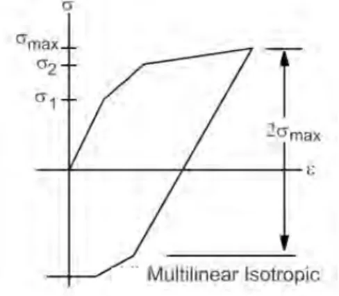
Material Models
The hardening rule is defined by changing the plastic surface with progressive yielding so that stress states can be formed for subsequent yielding. The time-dependent evolution equation of the local atomic density induced by the applied current is the mass balance (continuity) equation. Therefore, in order to obtain a complete solution to the problem, we should determine in a connected way the evolution of the distributions of current, temperature and voltage in the considered segment, which are caused by the continuous redistribution of the density of atoms.
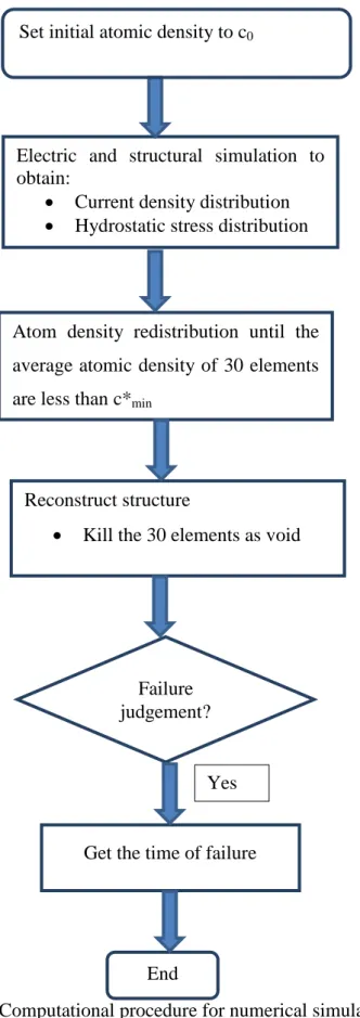
Thus, the normalized atomic density c in (i+1) steps can be obtained based on Eq. 33) in the form of the corresponding value in the i-th step. Lifetime and fault location in a solder bump can be predicted using numerical simulation of the process of cavity incubation, initiation and growth. In the simulation procedure for the cavity growth period, when the average atomic density value of the elements is less than the critical atomic density for cavity initiation c∗min, the corresponding elements will be killed ("element death"), and the structure presented in Figure 3.8 must be reconstructed.
In the semiconductor industry for an FCBGA solder bump failure criterion, a 15% increase in electrical resistance of the bump is usually considered EM failure.
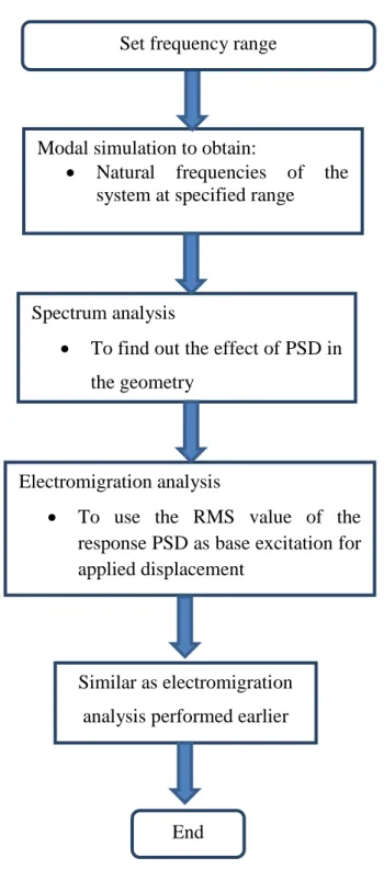
Simulation Methodology for Random Vibration Analysis
To use the RMS value of the response PSD as base excitation for applied displacement.
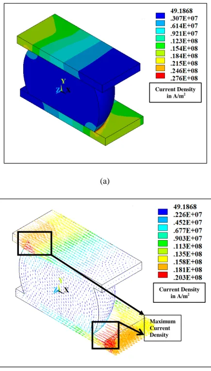
Current Density Distribution in the Solder Joint
This variation in electrical current is the sole function of the geometry of the solder joint and the Cu-pad interface. However, the initial electric current density varies linearly with the variation of electric current, which is verified from the plot of maximum current density variation with electric current as shown in Figure 4.2. It is further observed in Figure 4.2 that the maximum electrical current density occurring at the time of solder joint failure appears to be a function of some other parameters such as material properties etc.
That is why the electric current density at the time of the fault varies in a different way compared to the original current density with the variation of the electric current. The maximum current density is observed at the base of Cu and SAC material where the voids merge to form an open circuit.
Effects of Current Density
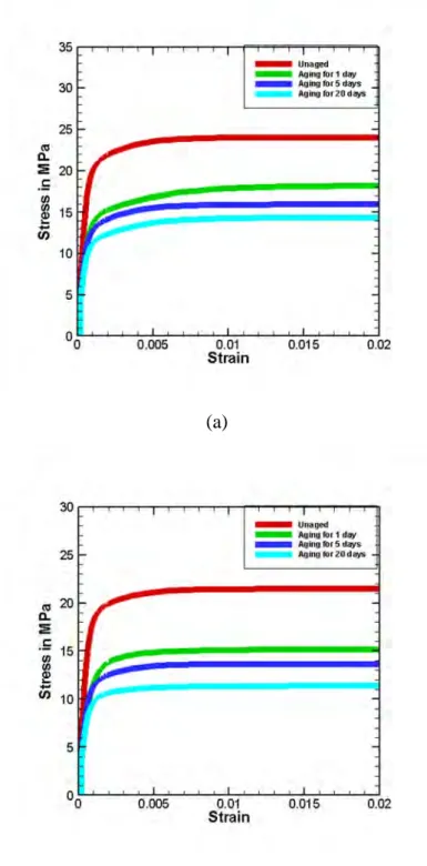
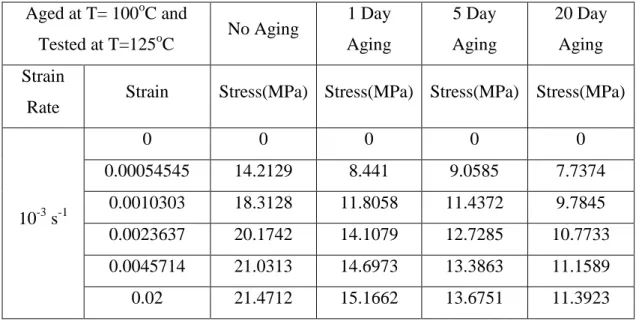
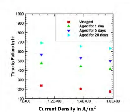
As the plot reveals, the diffusion flux increases about 6-8 times with the increase in solder joint ambient temperature from 100oC to 125oC. This distribution shows that diffusion flux has a proportional relationship with the electrical current density, which means that more electrons pass through the SAC solder joint. From Figure 4.9(a), it can be observed that with the increase of the aging time from 24 hours to 480 hours, the maximum diffusion flux decreases by approx. 20%.
Moreover, from Figure 4.9(b), a greater amount of diffusion flux can be observed at a higher electromigration temperature (125oC) due to the increased amount of kinetic energy obtained due to electron movement at higher temperatures. These thick grain boundaries actually dominate the grain boundary diffusion in SAC solder joint material. From Figure 4.14, the variation of electromigration-directed mass diffusion in terms of Ag percentage is summarized for investigation.
So it can be definitely stated that increasing Ag percentage reduces the electromigration lifetime of the SAC solder joint.
Effects of Thermal Aging on Electromigration Life
With the temperature increase to 125oC, the hydrostatic pressure increases during different aging periods. The time required to cause such a resistance change is marked as the time to failure (TTF) of the solder joint. Since at elevated temperature the grain boundary diffusion process is most dominant for mass diffusion, this reduction of the grain boundary area and the coarsening of the Sn-based microstructure causes an increase in the electromigration lifetime.
This grain boundary reduction is governed by the elastic modulus values as well as the stress strain properties of the SAC solder material under different thermal aging conditions. Due to the coarsening of the microstructure of the Sn-rich SAC solder material, the structural properties deteriorate significantly. This degradation of structural properties affects stress migration and subsequent mass diffusion in the SAC solder joint.
Thus, thermal aging plays an important role in the case of increasing the electromigration life of a SAC305 solder joint.
Effect of IMC Formation on Thermally Long Aged Solder Joints
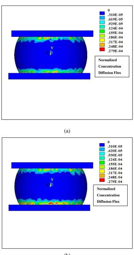
It shows that diffusion flux is significantly lower in most of the area of the SAC solder joint. Intermetallics such as Cu3Sn and Cu6Sn5 are essentially present in SAC solder joints under thermal aging conditions exposed for a long time. This brittle layer of IMC blocks the electromigration-oriented mass diffusion at the interface between the solder and Cu pads.
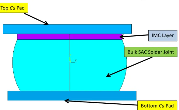
Since the IMC layer is linear elastic in nature, it does not exhibit inelastic work dissipation, similar to the Cup pad in previous studies. In this study, a single layer of intermetallic compound is placed between the top Cu pad and the SAC solder joint. In real applications, IMC layers are usually present at both interfaces of the SAC solder joint.
However, maintaining such layers on both sides of the solder joint will actually further reduce the diffusion flux and subsequent PLWK compared to the single layer IMC.
Numerical Validation
The finite element model of this research was used to predict the TTF of the SnPb solder joint (similar to the study done by Lin et al. [55]). For this purpose, the properties of SnPb solder materials from Wang et al. The TTF found from the FEA study is 104 minutes which is close to the experimental result of 95 minutes.
![Figure 4.28 Simulation Model capturing failure of SnPb solder joint Table 4.1 Electromigration and Mechanical Parameter of SnPb Solder Joint [63]](https://thumb-ap.123doks.com/thumbv2/filepdfnet/10888865.0/97.892.163.696.331.679/figure-simulation-capturing-failure-electromigration-mechanical-parameter-solder.webp)
Grid Independence Test
Modal Shapes of SAC Solder Joint
Effect of Random Vibration on Electromigration
75] it has been recognized that the random vibration-oriented failure pattern is somehow different from the failure pattern due to electromigration. Electromigration-oriented failure is mainly void-based failure, while random vibration-oriented failure is based on cracking. It can be seen from Figure 5.3 that the maximum PLWK achieved in the case of the combined mode is significantly higher compared to the pure electromigration mode.
The effect of thermal aging and random vibration on the electromigration-oriented failure has been studied in this section. The effect of Ag percentage and random vibration on the electromigration-oriented failure has been studied in this section. It can be seen from Figure 5.6 that the diffusion flux increases with the increase in Ag percentage in the SAC solder material.
Thus, it can be said that the effect of random vibration is more severe in SAC solder joints containing a higher percentage of Ag.
Conclusions
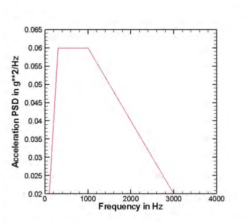
It has been shown in the study that the inelastic energy dissipation for SAC 305 solder joints decreases by 30-35% when the IMC thickness is increased to 4 microns from the unaged condition in the absence of intermetallics. The random vibration analysis showed that about 150% increase in inelastic energy dissipation and 80% increase in diffusion flux is observed for an input power spectrum density as shown in Figure 3.9. This concludes that random vibration reduces the electromigration life of a solder joint and can be considered a serious reliability problem.
This study will enable us to realize the effects of thermal aging, Ag percentage and random vibration on the electromigration-related mass diffusion in Flip-Chip SAC solder joints. It is expected that the results of this study will determine the optimal pre-aging time and Ag percentages for superior component design and thus optimize the reliability of Flip-Chip package solder joints.
Limitations of the Work
Since the TTF calculation is a highly time-consuming process with existing computational resources, electromigration lifetimes for SAC105 and 205 could not be calculated in this study.
Recommendation for Future Works
B., "Electromigration and Void Observation in Silver," J. og Nathan, M., "Numerical Simulation of Grain-Boundary Grooving by Level Set Method",'' J. Direct Observation of a Critical Length Effect in Dual-Damascene Cu/ Oxide Interconnects,'' Appl. 25] Arnaud, L., Berger, T., og Reimbold, G., "Beviser for korngrænse versus grænsefladediffusion i elektromigreringseksperimenter i kobberdamascene-forbindelser," J. J., "Reliability of the aging lead free solder joint," i 2006 E lectronic Components and T echnology Conference, Vol.
[53] Liu, Y., Zhang, Y., and Liang, L., “Prediction of electromigration induced voids and time to failure for the solder joint of a wafer-level chip-scale package,”. Improved reliability predictions of lead-free solder joints, including aging effects,” in Electronic Components and Technology Conference 2012, Vol. 63] Liu, Y., Zhang, Y., and Liang, L., “Prediction of electromigration induced voids and time to failure for the solder joint of a wafer-level chip-scale package,”.
64] Wang, S., Liang, L., and Liu, Y., "Reliability of solder joints under electromigration and thermal-mechanical loading", in 2006 Electronic Components and Technology Conference, Vol.