Fundamentals of Electronic Circuit Design
By
Hongshen Ma
© 2005 Hongshen Ma 2
Preface – Why Study Electronics?
Purely mechanical problems are often only a subset of larger multi-domain problems faced by the designer. Particularly, the solutions of many of today’s interesting problems require expertise in both mechanical engineering and electrical engineering.
DVD players, digital projectors, modern cars, machine tools, and digital cameras are just a few examples of the results of such combined innovation. In these hybrid systems, design trade-offs often span the knowledge space of both mechanical and electrical engineering. For example, in a car engine, is it more cost-effective to design a precise mechanical timing mechanism to trigger the firing of each cylinder, or is it better to use electronic sensors to measure the positions of each piston and then use a microprocessor to trigger the firing? For every problem, designers with combined expertise in mechanical and electrical engineering will be able to devise more ideas of possible solutions and be able to better evaluate the feasibility of each idea.
A basic understanding of electronic circuits is important even if the designer does not intend to become a proficient electrical engineer. In many real-life engineering projects, it is often necessary to communicate, and also negotiate, specifications between engineering teams having different areas of expertise. Therefore, a basic understanding of electronic circuits will allow the mechanical engineer to evaluate whether or not a given electrical specification is reasonable and feasible.
The following text is designed to provide an efficient introduction to electronic circuit design. The text is divided into two parts. Part I is a barebones introduction to basic electronic theory while Part II is designed to be a practical manual for designing and building working electronic circuits.
© 2005 Hongshen Ma 3
Part I
Fundamentals Principles
By
Hongshen Ma
© 2005 Hongshen Ma 4
Important note:
This document is a rough draft of the proposed
textbook. Many of the
sections and figures need to be revised and/or are
missing. Please check future
releases for more complete
versions of this text.
© 2005 Hongshen Ma 5
Fundamentals of Electronic Circuit Design
Outline
Part I – Fundamental Principles
1 The Basics
1.1 Voltage and Current 1.2 Resistance and Power 1.3 Sources of Electrical Energy 1.4 Ground
1.5 Electrical Signals
1.6 Electronic Circuits as Linear Systems
2 Fundamental Components: Resistors, capacitors, and Inductors 2.1 Resistor
2.2 Capacitors 2.3 Inductors
3 Impedance and s-Domain Circuits 3.1 The Notion of Impedance 3.2 The Impedance of a Capacitor 3.3 Simple RC filters
3.4 The Impedance of an Inductor 3.5 Simple RL Filters
3.6 s-Domain Analysis
3.7 s-Domain Analysis Example
3.8 Simplification Techniques for Determining the Transfer Function 3.8.1 Superposition
3.8.2 Dominant Impedance Approximation
3.8.3 Redrawing Circuits in Different Frequency Ranges 4 Source and Load
4.1 Practical Voltage and Current Sources 4.2 Thevenin and Norton Equivalent Circuits 4.3 Source and Load Model of Electronic Circuits 5 Critical Terminology
5.1 Buffer
5.2 Bias
5.3 Couple 6 Diodes
6.1 Diode Basics 6.2 Diode circuits
© 2005 Hongshen Ma 6 6.2.1 Peak Detector
6.2.2 LED Circuit
6.2.3 Voltage Reference 7 Transistors
7.1 Bipolar Junction Transistors 7.2 Field-effect Transistors 8 Operational Amplifiers
8.1 Op amp Basics 8.2 Op amp circuits
8.2.1 non-inverting amplifier 8.2.2 inverting amplifier 8.2.3 signal offset 9 Filters
9.1 The Decibel Scale
9.2 Single-pole Passive Filters 9.3 Metrics for Filter Design 9.4 Two-pole Passive Filters 9.5 Active Filters
9.5.1 First order low pass 9.5.2 First order high pass 9.5.3 Second order low pass 9.5.4 Second order high pass 9.5.5 Bandpass 10 Feedback
10.1 Feedback basics
10.2 Feedback analysis – Block diagrams 10.3 Non-inverting amplifier
10.4 Inverting amplifier 10.5 Precision peak detector 10.6 Opamp frequency response 10.7 Stability analysis
© 2005 Hongshen Ma 7 1 The Basics
1.1 Voltage and Current
Voltage is the difference in electrical potential between two points in space. It is a measure of the amount of energy gained or lost by moving a unit of positive charge from one point to another, as shown in Figure 1.1. Voltage is measured in units of Joules per Coulomb, known as a Volt (V). It is important to remember that voltage is not an absolute quantity; rather, it is always considered as a relative value between two points.
In an electronic circuit, the electromagnetic problem of voltages at arbitrary points in space is typically simplified to voltages between nodes of circuit components such as resistors, capacitors, and transistors.
Figure 1.1: Voltage V1 is the electrical potential gained by moving charge Q1 in an electric field.
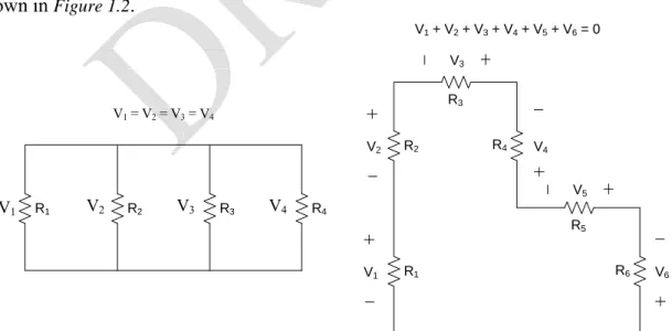
When multiple components are connected in parallel, the voltage drop is the same across all components. When multiple components are connected in series, the total voltage is the sum of the voltages across each component. These two statements can be generalized as Kirchoff’s Voltage Law (KVL), which states that the sum of voltages around any closed loop (e.g. starting at one node, and ending at the same node) is zero, as shown in Figure 1.2.
R2 R4
R3
R1
R5
R6
V1
V2
V3
V5
V4
V6
V1 + V2 + V3 + V4 + V5 + V6 = 0
R1
V1 V2 R2 V3 R3 V4 R4
V1 = V2 = V3 = V4
Figure 1.2: Kirchoff’s Voltage Law: The sum of the voltages around any loop is zero.
Electric current is the rate at which electric charge flows through a given area.
Current is measured in the unit of Coulombs per second, which is known as an ampere
© 2005 Hongshen Ma 8
(A). In an electronic circuit, the electromagnetic problem of currents is typically simplified as a current flowing through particular circuit components.
+ +
+ + +
+ +
+
+ + + +
+ + +
+ + +
+
+ +
+ +
+
+
+ + + +
+ + +
+
+
+
+
+ + ++
+ +
+ +
+ + +
+ + +
+ + +
+
+ + + +
+
+
+
+
I 1
+Figure 1.3: Current I1 is the rate of flow of electric charge
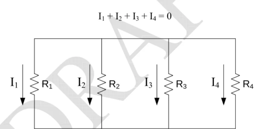
When multiple components are connected in series, each component must carry the same current. When multiple components are connected in parallel, the total current is the sum of the currents flowing through each individual component. These statements are generalized as Kirchoff’s Current Law (KCL), which states that the sum of currents entering and exiting a node must be zero, as shown in Figure 1.4.
R1
I1 I2 R2 I3 R3 I4 R4
I1 + I2 + I3 + I4 = 0
Figure 1.4: Kirchoff’s Current Law – the sum of the currents going into a node is zero.
An intuitive way to understand the behavior of voltage and current in electronic circuits is to use hydrodynamic systems as an analogue. In this system, voltage is represented by gravitational potential or height of the fluid column, and current is represented by the fluid flow rate. Diagrams of these concepts are show in Figure 1.5 through 1.7. As the following sections will explain, electrical components such as resistors, capacitors, inductors, and transistors can all be represented by equivalent mechanical devices that support this analogy.
© 2005 Hongshen Ma 9
height = V
1height = V
2Figure 1.5: Hydrodynamic analogy for voltage
Current
Figure 1.6: Hydrodynamic analogy for current
height = V
Cur ren t
Figure 1.7: A hydrodynamic example representing both voltage and current
1.2 Resistance and Power
When a voltage is applied across a conductor, a current will begin to flow. The ratio between voltage and current is known as resistance. For most metallic conductors, the relationship between voltage and current is linear. Stated mathematically, this property is known as Ohm’s law, where
© 2005 Hongshen Ma 10 R V
= I
Some electronic components such diodes and transistors do not obey Ohm’s law and have a non-linear current-voltage relationship.
The power dissipated by a given circuit component is the product of voltage and current,
P=IV
The unit of power is the Joule per second (J/s), which is also known as a Watt (W).
If a component obeys Ohm’s law, the power it dissipates can be equivalently expressed as,
P=I R2 or V2
P= R . 1.3 Voltage and Current Sources
There are two kinds of energy sources in electronic circuits: voltage sources and current sources. When connected to an electronic circuit, an ideal voltage source maintains a given voltage between its two terminals by providing any amount of current necessary to do so. Similarly, an ideal current source maintains a given current to a circuit by providing any amount of voltage across its terminals necessary to do so.
Voltage and current sources can be independent or dependent. Their respective circuit symbols are shown in Figure 1.8. Independent sources are usually shown as a circle while dependent sources are usually shown as a diamond-shape. Independent sources can have a DC output or a functional output; some examples are a sine wave, square wave, impulse, and linear ramp. Dependent sources can be used to implement a voltage or current which is a function of some other voltage or current in the circuit.
Dependent sources are often used to model active circuits that are used for signal amplification.
VS IS
VS=f(V1)
or
VS=f(I1)
IS=f(V1)
or
IS=f(I1)
Figure 1.8: Circuit symbols for independent and dependent voltage and current sources
© 2005 Hongshen Ma 11 1.4 Ground
An often used and sometimes confusing term in electronic circuits is the word ground. The ground is a circuit node to which all voltages in a circuit are referenced. In a constant voltage supply circuit, one terminal from each voltage supply is typically connected to ground, or is grounded. For example, the negative terminal of a positive power supply is usually connected to ground so that any current drawn out of the positive terminal can be put back into the negative terminal via ground. Some circuit symbols used for ground are shown in Figure 1.9.
Figure 1.9: Circuit symbols used for ground
In some circuits, there are virtual grounds, which are nodes at the same voltage as ground, but are not connected to a power supply. When current flows into the virtual ground, the voltage at the virtual ground may change relative to the real ground, and the consequences of this situation must be analyzed carefully.
1.5 Electronic Signals
Electronic signals are represented either by voltage or current. The time- dependent characteristics of voltage or current signals can take a number of forms including DC, sinusoidal (also known as AC), square wave, linear ramps, and pulse- width modulated signals. Sinusoidal signals are perhaps the most important signal forms since once the circuit response to sinusoidal signals are known, the result can be generalized to predict how the circuit will respond to a much greater variety of signals using the mathematical tools of Fourier and Laplace transforms.
A sinusoidal signal is specified by its amplitude (A), angular frequency (ω), and phase (φ) as,
( )
( ) sin
V t = A ω φt+
When working with sinusoidal signals, the mathematical manipulations often involves computing the effects of the circuit on the amplitude and phase of the signal, which can involve cumbersome trigonometric identities. Operations involving sinusoidal functions can be greatly simplified using the mathematical construct of the complex domain (see Appendix for more information). The sinusoidal signal from the above equation, when expressed in the complex domain, becomes the complex exponential,
( ) j t
V t =Ae−ω ,
© 2005 Hongshen Ma 12
where the physical response is represented by the real part of this expression. The amplitude and phase of the signal are both described by the complex constant A, where
j A
A= A e−φ .
As the following section will show, the complex representation of electronic signals greatly simplifies the analysis of electronic circuits.
1.6 Electronic Circuits as Linear Systems
Most electronic circuits can be represented as a system with an input and an output as shown in Figure 1.10. The input signal is typically a voltage that is generated by a sensor or by another circuit. The output signal is also often a voltage and is used to power an actuator or transmit signals to another circuit.
Circuit
Sensor Actuator
Input Signal Output Signal
Figure 1.10: Electronic circuit represented as a linear system
In many instances, it is possible to model the circuit as a linear system, which can be described by the transfer function H, such that
out in
H V
= V .
For DC signals, the linearity of the system implies that H is independent of Vin. For dynamic signals, the transfer function cannot in general be described simply.
However, if the input is a sinusoidal signal then the output must also be a sinusoidal signal with the same frequency but possibly a different amplitude and phase. In other words, a linear system can only modify the amplitude and phase of a sinusoidal input. As a result, if the input signal is described as a complex exponential,
( ) j ot
V tin = Ae−ω , where A is a complex constant,
j A
A= A e−φ .
The transfer function H can be entirely described by a complex constant,
© 2005 Hongshen Ma 13
j H
H = H e−φ , and the output signal is simply
( ) j ot
Vout t =HAe−ω , or in expanded form,
( A ) o
j j
( ) H t
Vout t = H A e− φ φ+ e−ω .
In general, the sinusoidal response of linear systems is not constant over frequency and H is also a complex function of ω.
© 2005 Hongshen Ma 14
2 Fundamental Components: Resistors, Capacitors, and Inductors
Resistors, capacitors, and inductors are the fundamental components of electronic circuits. In fact, all electronic circuits can be equivalently represented by circuits of these three components together with voltage and current sources.
2.1 Resistors
Resistors are the most simple and most commonly used electronic component.
Resistors have a linear current-voltage relationship as stated by Ohm’s law. The unit of resistance is an ohm, which is represented by the letter omega (Ω). Common resistor values range from 1 Ω to 22 MΩ.
In the hydrodynamic analogy of electronic circuits, resistors are equivalent to a pipe. As fluid flows through a pipe, frictional drag forces at the walls dissipate energy from the flow and thus reducing the pressure, or equivalently, the potential energy of the fluid in the pipe. A small resistor is equivalent to a large diameter pipe that will allow for a high flow rate, whereas a large resistor is equivalent to a small diameter pipe that greatly constricts the flow rate, as shown in Figure 2.1.
Figure 2.1: The hydrodynamic model of a resistor is a pipe
When several resistors are connected in series, the equivalent resistance is the sum of all the resistances. For example, as shown in Figure 2.2,
1 2
Req =R +R
When several resistors are connected in parallel, the equivalent resistance is the inverse of the sum of their inverses. For example,
3 4
3 4
3 4
1
1 1
eq
R R R
R R
R R
= =
+ +
In order to simplify this calculation when analyzing more complex networks, electrical engineers use the || symbol to indicate that two resistances are in parallel such that
3 4 3 4
3 4
3 4
|| 1
1 1
R R R R
R R
R R
= =
+ +
© 2005 Hongshen Ma 15
R3 R4
R1
R2
Figure 2.2: Resistors in series and in parallel
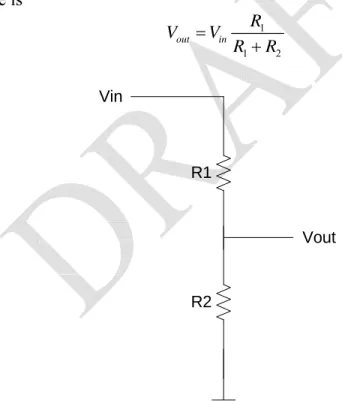
A common resistor circuit is the voltage divider used to divide a voltage by a fixed value. As shown in Figure 2.3, for a voltage Vin applied at the input, the resulting output voltage is
1
1 2
out in
V V R
R R
= +
R1
R2 Vin
Vout
Figure 2.3: Voltage divider circuit 2.2 Capacitors
A capacitor is a device that stores energy in the form of voltage. The most common form of capacitors is made of two parallel plates separated by a dielectric material. Charges of opposite polarity can be deposited on the plates, resulting in a
© 2005 Hongshen Ma 16
voltage V across the capacitor plates. Capacitance is a measure of the amount of electrical charge required to build up one unit of voltage across the plates. Stated mathematically,
C
C Q
=V ,
where Q is the number of opposing charge pairs on the capacitor. The unit of capacitance is the Farad (F) and capacitors are commonly found ranging from a few picofarads (pF) to hundreds of microfarads (μF).
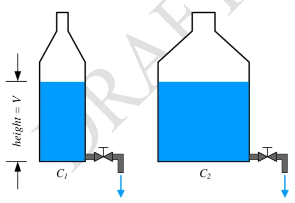
In the hydrodynamic analogy to electronic circuits, a capacitor is equivalent to a bottle, as shown in Figure 2.4. The voltage across the capacitor is represented by the height of fluid in the bottle. As fluid is added to the bottle, the fluid level rises just as charges flowing onto the capacitor plate build up the voltage. A small capacitor is a thin bottle, where adding a small volume of fluid quickly raise the fluid level.
Correspondingly, a large capacitor is a wide bottle, where a larger volume of fluid is required to raise the fluid level by the same distance.
height = V
C
1C
2Figure 2.4: The hydrodynamic model of a capacitor is a bottle
The current-voltage relationship of the capacitor is obtained by differentiating Q=CV to get
dVC
I dQ C
dt dt
= = .
© 2005 Hongshen Ma 17
Unlike a resistor, current in a capacitor is proportional to the derivative of voltage rather than voltage itself. Alternatively, it can be said that the voltage on a capacitor is proportional to the time integral of the influx current.
VC =
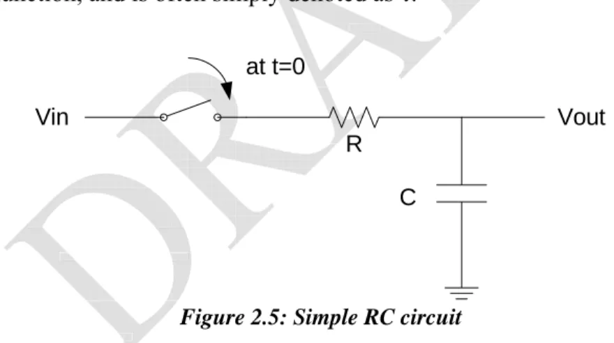
∫
IdtA typical example of a capacitor circuit is shown in Figure 2.5, where the capacitor is connected in series with a resistor, a switch, and an ideal voltage source.
Initially, for t<0, the switch is open and the voltage on the capacitor is zero. The switch closes at t=0, the voltage drop across the resistor is Vin−VC, and charges flows onto the capacitor at the rate of
(
Vin −VC)
/R . As voltage builds on the capacitor, the corresponding voltage on the resistor is therefore decreased. The reduction in voltage leads to a reduction of the current through the circuit loop and slows the charging process.The exact behavior of voltage across the capacitor can be found by solving the first order differential equation,
C S C
dV V V
C dt R
= − .
The voltage across the capacitor behaves as an exponential function of time, which is shown in Figure ###. The term RC, is known as the time constant of the exponential function, and is often simply denoted as τ.
R C
Vin Vout
at t=0
Figure 2.5: Simple RC circuit (### insert plot of RC response here ###)
Figure ###: Voltage output for the RC circuit as a function of time 2.3 Inductor
An inductor is a device that stores energy in the form of current. The most common form of inductors is a wire wound into a coil. The magnetic field generated by the wire creates a counter-acting electric field which impedes changes to the current. This effect is known as Lenz’s law and is stated mathematically as
L
V LdI
= − dt .
© 2005 Hongshen Ma 18
The unit of inductance is a Henry (H) and common inductors range from nanohenries (nH) to microhenries (μH).
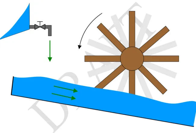
In the hydrodynamic analogy of electronic circuits, an inductor can be thought of as a fluid channel pushing a flywheel as shown in Figure 2.6. When the fluid velocity (current) in the channel changes, the inertia of the flywheel tends to resist that change and maintain its original angular momentum. A large inductor corresponds to a flywheel with a large inertia, which will have a larger influence on the flow in the channel.
Correspondingly a small inductor corresponds to a flywheel with a small inertia, which will have a lesser effect on the current.
Figure 2.6: Hydrodynamic analogy of an inductor is a flywheel
An example of the time domain analysis of an inductor circuit is shown in Figure 2.7 where the inductor is connected in series with a resistor, a switch, and an ideal voltage source. Initially, the current through the inductor is zero and the switch goes from closed to open at t=0. Similar to the capacitor-resistor circuit, the time-domain behavior of this circuit can be determined by solving the first order differential equation ###. The resulting voltage across the inductor is an exponential function of time as shown in Figure ###.
© 2005 Hongshen Ma 19 R
C
Vin Vout
at t=0
Figure 2.7: Simple RL circuit
###insert V(t) plot###
Figure ###: Voltage output for the RL circuit as a function of time
Switching circuits involving inductors have a rather destructive failure mode.
Suppose that in the circuit shown in Figure ###, the switch is opened again after the current flowing through the inductor has reached steady-state. Since the current is terminated abruptly, the derivative term of Eq. ### can be very high. High voltages can result in electrical breakdown which can permanently damage the inductor as well as other components in the circuit. This problem and appropriate remedies are discussed in more detail in section 18.2.
© 2005 Hongshen Ma 20 3 Impedance and s-Domain Circuits 3.1 The Notion of Impedance
Impedance is one of the most important concepts in electronic circuits. The purpose of impedance is to generalize the idea of resistance to create a component, shown in Figure 3.1, to capture the behavior of resistors, capacitors, and inductors, for steady- state sinusoidal signals. This generalization is motivated by the fact that as long as the circuit is linear, its behavior can be analyzed using KVL and KCL.
ZLOAD
IIN
VIN
Figure 3.1: Impedance – a generalized component
Impedance essentially can be viewed as frequency-dependent resistance. While resistance of a circuit is the instantaneous ratio between voltage and current, impedance of a circuit is the ratio between voltage and current for steady-state sinusoidal signals, which can vary with of frequency. As the later parts of this section will show, the voltage and current caused by applying a steady-state sinusoidal signal to any combination of resistors, capacitors, and inductors, are related by a constant factor and a phase shift.
Therefore, impedance can be expressed by a complex constant using an extended version Ohm’s law,
( ) ( )
( ) Z V
I ω ω
= ω ,
Where V(ω) and I(ω) are both the complex exponential representations of sinusoidal functions as disused in the next section.
The real part and imaginary part of impedance are interpreted as a resistive part that dissipates energy and a reactive part that stores energy. Resistors can only dissipate energy and therefore their impedances have only a real part. Capacitors and inductors can only store energy and therefore their impedances have only an imaginary part. When resistors, capacitors, and inductors are combined, the overall impedance may have both real and imaginary parts. It is important to note that the definition of impedance preserves the definition of resistance. Therefore, for a circuit with only resistors, ZEQ = REQ.
###An intuitive mechanical analog of impedance is stiffness. Stiffness is defined as the ratio between stress and strain, which in a practical mechanical structure can be measured as force and deflection. ###
© 2005 Hongshen Ma 21 3.2 The Impedance of a Capacitor
The impedance of a capacitor is determined by assuming that a sinusoidal voltage is applied across the capacitor, such that
j t
VC = Aeω . Since
C C
I CdV
= dt , the resulting current is
j t
IC = j CAeω ω .
Therefore, the impedance, or the ratio between voltage and current, is
C 1
C C
Z V
I j Cω
= = .
From the above equation, it is possible to see that the impedance of a capacitor is a frequency-dependent resistance that is inversely proportional to frequency; ZC is small at high frequency and large at low frequency. At DC, the impedance of a capacitor is infinite. The impedance expression also indicates that for a sinusoidal input, the current in a capacitor lags its voltage by a phase of 90o.
3.3 Simple RC Filters
A simple low-pass filter circuit, which allows low frequency signals to pass through the circuit while attenuating high-frequency signals, can be made using a resistor and capacitor in series as shown in Figure 3.2. The transfer function of this filter can be determined by analyzing the circuit as a voltage divider,
1
1
1 1
out in
V j C
V R j RC
j C ω
ω ω
= =
+ + .
The magnitude and phase of the frequency response of the low-pass filter are shown in Figure ###. The magnitude response is shown on a log-log scale, whereas the phase response is shown on a linear-log scale. For ω>>RC, the denominator of the transfer function is much greater than one and the input is significantly attenuated. On the other hand, for, Vout ≅Vin . The transition point between the high and low frequency regions is defined when ωRC=1, where Vout/Vin =1/ 2. This is known as the cut-off frequency for the filter,
© 2005 Hongshen Ma 22 1
C RC
ω = .
R C
Vin Vout
Figure 3.2: Simple RC low-pass filter
###(Insert Figure Here)
Figure ###: The frequency response of a simple RC low-pass filter
A simple high-pass filter can be made by switching the positions of the capacitor and resistor in the low-pass filter. The transfer function is now
1 1
out in
V R j RC
V R j RC
j C
ω ω ω
= =
+ + .
The frequency response of the high-pass filter is shown in Figure 3.3. Similar to the low-pass filter, the high-pass filter has a cut-off frequency at ωC =1/RC.
R C
Vin Vout
Figure 3.3: Simple RC high-pass filter
###(Insert Figure Here)
Figure ###: The frequency response of a simple RC high-pass filter
© 2005 Hongshen Ma 23 3.4 The Impedance of an Inductor
The ratio between voltage and current for an inductor can be found in a similar way as for a capacitor. For a sinusoidal voltage,
j t
VL = Aeω . Since
L L
I LdV
= dt ,
j t
IL = j LAeω ω . Thus, the impedance of an inductor is
L L
L
Z V j L
I ω
= = .
Therefore, an inductor is a frequency-dependent resistance that is directly proportional to frequency; ZL is small at low frequency and large at high frequency. At DC, the impedance of an inductor is zero. Just as for a capacitor, this expression shows that the voltage across an inductor lags the current by a phase of 90o.
3.5 Simple RL Filters
A low-pass filter can also be made using a resistor and an inductor in series, as shown in Figure 3.4. Once again, the transfer function of this filter can be determined like a voltage divider,
1 1
out in
V R
V R j L j L
R ω ω
= =
+ +
.
R L
Vout
Vin
Figure 3.4: Simple RL low-pass filter
###(Insert Figure Here)
Figure ###: The frequency response of a simple RL low-pass filter
© 2005 Hongshen Ma 24
The magnitude and phase of the frequency response are shown in Figure ###. For /
ω>>R L, Vout is attenuated, whereas for ω<<R L/ , Vout ≅Vin. At the cut-off frequency,
2 2
c
c R
f L
ω π π
= = ,
L 1 R ω =
, and 1
2
out in
V
V = .
A high-pass RL filter can be made from the low-pass RL filter by switching the position of the inductor and resistor as shown in Figure 3.5. The transfer function is
1
out in
j L
V j L R
V R j L j L
R ω ω
ω ω
= =
+ +
.
R
L
Vout
Vin
Figure 3.5: Simple RL high-pass filter
###(Insert Figure Here)
Figure ###: The frequency response of a simple RL high-pass filter
The frequency response of the filter is shown in Figure ###. The cut-off frequency of the high-pass filter is the same as the low-pass filter (Eq. ###)
3.6 s-Domain Analysis
The concept of complex impedance introduces a unified representation for resistors, capacitors, and inductors, whereby a circuit’s frequency response from input to output can be determined using KVL and KCL, where each element is assigned the appropriate impedance. The key assumption to this point is that the input to the circuit must consist solely of DC and/or sinusoidal signals. Now, this analysis is be extended to include arbitrary input signals by using the mathematical techniques of Laplace transforms.
© 2005 Hongshen Ma 25
The “brute force” method for determining the response of a circuit to an arbitrary signal is to write a system of linear differential equations using the voltage and current variables in the circuit and then to solve for the output signal, using the input signals as the forcing functions. The Laplace transform simplifies this process by converting linear differential equations in the time domain to algebraic equations in the complex frequency domain. The independent variable in the complex frequency domain is s, where
s= +σ jω.
The process for solving differential equations using Laplace transforms involves the following general procedure:
1. Write a set of differential equations to describe the circuit;
2. Laplace transform the differential equations to algebraic equations in s- domain;
3. Solve for the transfer function in the s-domain;
4. Laplace transform the input signal and multiply this by the transfer function to give the output signal in the s-domain;
5. Inverse Laplace transform the output signal to give circuit response as a function in the time domain.
The determination of the transfer function in steps 2 and 3 of this procedure can be greatly simplified by Laplace transforming of the impedances of individual circuit elements instead of generalized differential equations that govern circuit behavior. The transfer function can then be found by applying KVL and KCL simplifications to the resulting “Laplace circuit”.
For example, the current-voltage relationship of a capacitor is C dVC I C
= dt and the Laplace transformed result is IC =sCVC. Therefore, the impedance of a capacitor in s- domain is 1/sC. Similarly for an inductor, L dIL
V L
= dt and the Laplace transform of this is VL =sLIL. Therefore, the s-domain impedance for an inductor is sL. For a resistor, the s-domain impedance is still R. A summary of the s-domain representation of electronic circuits is shown in Table 3.1. Interestingly, the s-domain impedance very closely resembles the complex impedances discussed previously. In fact, the s-domain impedance is an extended version of the complex impedance that generalizes to arbitrary signals.
Time Domain Parameter s-Domain Impedance
R R C 1/sC L sL Table 3.1: Summary of s-domain impedances
© 2005 Hongshen Ma 26
The impedance representation once again unifies resistors, capacitors, and inductors as equivalent circuit components with specific impedances and the s-domain transfer function can be found by using KVL and KCL. The transfer function is generally expressed as a ratio of polynomials such that
( ) ( )
out in
V Z s V = P s , where
1
1 2 1
( ), ( ) n n ... n n
Z s P s =a s +a s − +a −s+a .
The polynomial can be factored into a number of roots. The roots of the denominator polynomial are known as poles, while the roots of the numerator polynomial are known as zeros.
The frequency response of the circuit is obtained by substituting jω for s in the transfer function. The time-domain response is found by implementing steps 4 and 5 of the general procedure: take the Laplace transform of the input signal and then take the inverse Laplace transform of the output signal. In practice, step 4 can be simplified since the time-domain behavior of a circuit is almost always evaluated in response to a step or ramp voltage input, for which the inverse Laplace transforms can be easily computed or obtained from existing tables. Step 5 is also usually simplified since most transfer functions can be approximated by one of a few transfer functions which have known time-domain responses to step and ramp input signals.
3.7 s-Domain Analysis Example
3.8 Simplification Techniques for Determining the Transfer Function 3.8.1 Superposition
3.8.2 Dominant Impedance Approximation
3.8.3 Redrawing Circuits in Different Frequency Ranges
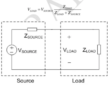
© 2005 Hongshen Ma 27 4 Source and Load
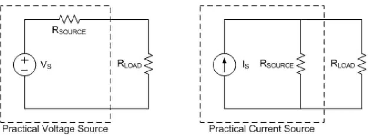
The ideas of electrical source and load are extremely useful constructs in circuit analysis since all electronic circuits can be modeled as a source circuit, a load circuit, or some combination of the two. Source circuits are circuits that supply energy while load circuits are circuits that dissipate energy. Load circuits can be simply modeled by a single equivalent impedance, while source circuits can be modeled as a voltage or current source plus an equivalent impedance. This section describes the properties of practical voltage and current sources; how to represent the output of arbitrary circuits as source circuits; and how the source and load model of electronic circuits can be used to model circuit behavior.
4.1 Practical Voltage and Current Sources
As discussed in section 1.3, an ideal voltage source will maintain a given voltage across a circuit by providing any amount of current necessary to do so; and an ideal current source will supply a given amount of current to a circuit by providing any amount of voltage output necessary to do so. Of course, ideal voltage sources and ideal current sources are both impossible in practice. When a very small resistive load is connected across an ideal voltage source, a practically infinite amount of current is required.
Correspondingly, when a large resistive load is connected across an ideal current source, an exceedingly large voltage is required.
A practical voltage source is modeled as an ideal voltage source in series with a small source resistance, as shown in Figure 4.1. The output voltage across the load resistance is attenuated due to the source resistance and the resulting voltage is determined by the resistive divider,
LOAD
out S
LOAD SOURCE
V V R
R R
= + .
A practical voltage source can approach an ideal voltage source by lowering its source resistance. Therefore, ideal voltage sources are said to have zero source resistance.
© 2005 Hongshen Ma 28
Figure 4.1: Practical voltage and current sources
A practical current source is modeled as an ideal current source in parallel with a large source resistance. The output current is reduced due to the source resistance by the current divider such that,
SOURCE
out S
LOAD SOURCE
I I R
R R
= + .
A practical current source can approach an ideal current source by increasing its source resistance. Therefore, ideal current sources are said to have infinite source resistance.
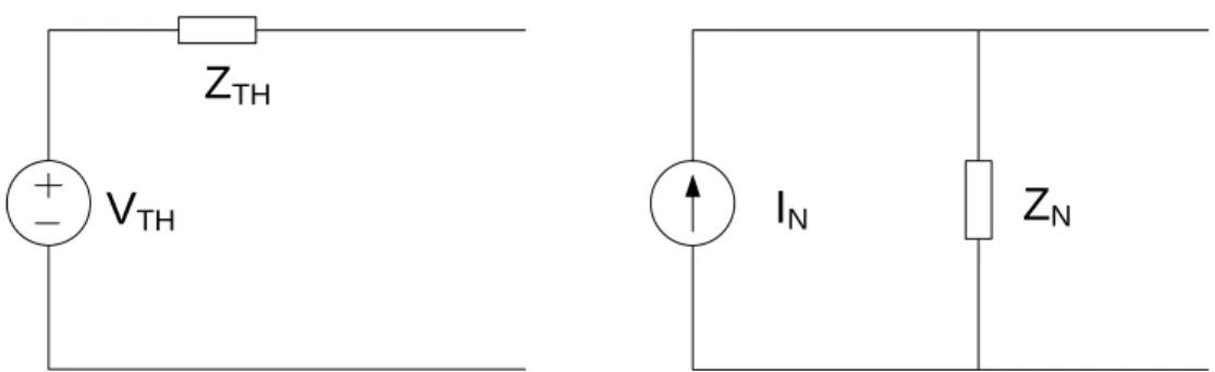
4.2 Thevenin and Norton Equivalent Circuits
The practical voltage and current source model can be used to model arbitrary linear source circuits using a technique known as Thevenin and Norton equivalent circuits.
Thevenin’s theorem states that the output of any circuit consisting of linear components and linear sources can be equivalently represented as a single voltage source, VTH, and a series source impedance, ZTH, as shown in Figure 4.2.
Norton’s theorem states that the output of any circuit consisting of linear components and linear sources can be equivalently represented as a single current source, IN, and a parallel source impedance, ZN, also shown in Figure 4.2.
I
NV
THZ
THZ
NFigure 4.2: Thevenin and Norton Equivalent Circuits
© 2005 Hongshen Ma 29
There are simple procedures to determine VTH, IN, ZN, and ZTH for a given circuit.
To determine VTH, set the load as an open circuit. The voltage across the output is VTH. To determine IN, set the load as a short circuit, and then the current through the short circuit is IN. An important link between Thevenin and Norton equivalent circuits is that ZTH and ZN are exactly the same value. To determine ZTH or ZN, short-circuit the voltage sources and open-circuit the current sources in the circuit. ZTH or ZN is then the resulting equivalent impedance of the circuit.
### Need Example circuit here with procedure for determining Thevenin and Norton equivalent circuits.###
4.3 Source and Load Model of Electronic Circuits
The simple model of source and load, shown in Figure 4.3, is an extremely useful way to predict how two circuits will interact when connected together. The source part can be used to represent the output of a circuit, while the load can be used to represent the input of another circuit. The value of ZLOAD can be determined from the equivalent circuit model of the load circuit using KVL and KCL. The value of ZSOURCE can be determined by Thevenin and Norton equivalent circuits. The voltage across the load can simply be calculated from,
LOAD
LOAD SOURCE
LOAD SOURCE
V V Z
Z Z
= +
Figure 4.3: Source and load model
The source and load model is particularly useful when the design of either the source or load circuit is fixed and a circuit is required to be the corresponding source or load circuit. For example, if the output of a voltage amplifier behaves as a voltage source with a source resistance of 500Ω, the input resistance of the next circuit, being the load impedance, should be significantly greater than 500Ω in order to prevent the source voltage from being attenuated.
© 2005 Hongshen Ma 30 5 Critical Terminology
As with any engineering discipline, electrical engineering is full of its own special words and lingo that can make electrical engineering speak sound like a foreign tongue.
Buffer, bias, and couple are three such words that can often trip-up new comers.
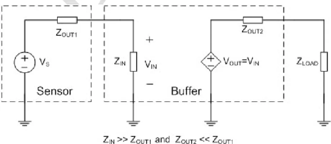
5.1 Buffer
Buffer is one of those words that seem to have a different meaning in every discipline of science and engineering. Buffer has two meanings in electrical engineering depending if the context is analog or digital electronics.
In analog electronics, to buffer means to preserve the content of a low power signal and convert it to a higher power signal via a buffer amplifier. This is a frequent operation in analog electronics since low power signals can be more easily interfered with than high power signals, but often only low power signals are available from electronic sensors.
If signals are represented by voltage in a circuit, the power of the signal is proportional to the amount of current drawn by the circuit. Since current draw is dependent on the impedance of the circuit, a high impedance circuit has less power, while a low impedance circuit has more power. The function of a buffer amplifier in this case is to convert a high impedance circuit to a low impedance circuit. This buffering scenario is represented by an equivalent circuit shown in Figure 5.1 where a voltage output electronic sensor has relatively high output impedance ZOUT1. If the sensor output is used to drive a load impedance, ZLOAD, directly, much of the voltage signal may be lost to attenuation. In order to remedy this problem, a buffer amplifier is inserted between the sensor output and ZLOAD. The input of the buffer amplifier measures this voltage signal with a high input impedance ZIN, and replicates the signal VIN with an output impedance ZOUT2. Since ZOUT2 is smaller than ZOUT1, the sensor signal can be used to drive ZLOAD without suffering significant attenuation.
Figure 5.1: A Functional Equivalent of a Buffer in Analog Electronics
© 2005 Hongshen Ma 31
In digital electronics, buffer refers to a mechanism in the communications link between two devices. When there are time-lags between the transmitting device and the receiving device, some temporary storage is necessary to store the extra data that can accumulate. This temporary storage mechanism is known as a buffer. For example, there is a buffer between the keyboard and the computer so that the CPU can finish one task before accepting more input to initiate another task. Digital video cameras have a much larger buffer to accumulate raw data from the camera before the data can be compressed and stored in a permanent location.
5.2 Bias
Bias refers to the DC voltage and current values in a circuit in absence of any time-varying signals. In circuits that contain nonlinear components such as transistors and diodes, it is usually necessary to provide a power supply with static values of voltage and current. These static operating parameters are known as the bias voltage and bias current of each device. When analyzing circuit response to signals, the circuit components are typically linearized about their DC bias voltage and current and the input signals are considered as linear perturbations. Frequently, the AC behavior of a circuit component is dependent on its bias voltage and bias current.
5.3 Couple
The word couple means to connect or to link a signal between two circuits. There are generally two types of coupling: DC and AC. As shown in Figure 5.2, DC coupling refers a direct wire connection between two circuits; while AC coupling refers to two circuits connected via a capacitor. Between AC coupled circuits, signals at frequencies below some cut-off frequency will be progressively attenuated at lower frequencies. The cut-off frequency is determined by the coupling capacitance along with the output impedance of the transmitting circuit and the input impedance of the receiving circuit.
Oscilloscope inputs also have both AC and DC coupling options, which allow the user the select between viewing the total signal or just the time-varying component. In addition to describing intentional circuit connections, AC coupling also refers to the path of interference signals through stray capacitances in the physical circuit. There are also a number of other coupling mechanisms not included in this discussion, such as magnetic, optical, and radio-frequency coupling.
Figure 5.2: DC and AC coupled circuits
© 2005 Hongshen Ma 32 6 Diodes
6.1 Diode Basics
A Diode is an electronic equivalent of a one-way valve; it allows current to flow in only one direction. There are two terminals on a diode, which are known as the anode and cathode. Current is only allowed to flow from anode to cathode. The symbol and drawing for the diode are shown in Figure 6.1 and Figure 6.2. The dark band of the diode drawing indicates the cathode mark on the diode symbol. The direction of current flow is indicated by the direction of the triangle. An easy trick for remembering the direction of current flow is to remember that of the current flowing alphabetically, from the anode to the cathode.
Anode Cathode
Figure 6.1: Circuit symbol for a diode
Figure 6.2: 3D model of a diode, the dark band indicate cathode (Courtesy of Vishay Semiconductors)
The unidirectional conduction through a diode is explained by semiconductor physics. A diode is a junction between N-type and P-type semiconductors, typically fabricated in thin layers as shown in Figure 6.3. Both N-type and P-type materials are electrically neutral, but have different mechanisms of conduction. In N-type material, negatively charged electrons are mobile and are the majority current carriers. In P-type material, positively charged holes are mobile are the majority current carriers. Holes are actually temporary positive charges created by the lack of an electron; the details of this interpretation can be found in textbooks on semiconductor physics [Ref: Sedra and Smith].
Near the junction interface, electrons from the N-type region diffuse into the P- type region while holes from the P-type region diffuse into the N-type region. The diffused electrons and holes remain in a thin boundary layer around the junction known as the depletion layer shown in Figure 6.3. The excess of positive and negative charges create a strong electric field at the junction which acts as a potential barrier that prevent electrons from entering the P-type region and holes from entering the N-type region.
© 2005 Hongshen Ma 33
When a negative electric field is applied from anode to cathode, the depletion region enlarges and it becomes even more difficult to conduct current across the junction. This is the reverse-conducting state. When a positive electric field is applied from anode to cathode, the depletion region narrows and allows current to conduct from the anode to the cathode. This is the forward-conducting state.
+ -
+
+ + +
+
+ + + +
+
+ +
+
+ +
+
+ +
+ + +
+
+
+
+
- -
- - -
- -
-
- -
- -
-
- -
- - -
- - - -
- -
- -
- Depletion Region
- -
+ +
+
+ +
+ +
+ +
+
-
- - -
- - -
- -
- -
+ +
Internal voltage of the PN junction N-type P-type
Anode Cathode
V
x
+ -
+
+ + +
+
+ + + +
+
+ +
+
+ + +
+ + +
+ +
+
+ +
+
- -
- - -
- -
-
- -
- -
-
- -
- - - -
- - -
- -
- -
- Depletion Region
- -
+ + + + +
+ +
+ +
+
-
- - -
- - -
- -
- -
+ +
Internal voltage of the PN junction N-type P-type
V
x
Reverse biased Forward biased
Anode Cathode
Figure 6.3: PN Junction in a diode showing the depletion region
The current-voltage relationship for a diode is shown in Figure 6.4. The current is an exponential function of voltage such that
( ) t 1
V V
I V Io⎛e ⎞
= ⎜⎜⎝ − ⎟⎟⎠, and
t
V kT
=Q .
At 300 K room temperature, Vt = 26 mV. This means that for every increase of Vt
in voltage, the current drawn by the diode scales by a factor of e. For most design purposes, the detailed exponential behavior of a diode can be approximated as a perfect conductor above a certain voltage and a perfect insulator below this voltage (Figure 6.4).
This transition voltage is known as the “knee” or “turn-on” voltage. For silicon (Si) diodes, the knee voltage is 0.7 V; for Schottky barrier and germanium (Ge) diodes, the knee voltage is 0.3 V; and for gallium-arsenide (GaAs), gallium-nitride (GaN), and other hetero-junction light-emitting diodes, the knee voltage can range from 2 to 4 V.
When a reverse voltage is applied to a diode, the resistance of the diode is very large. The exponential current-voltage behavior predicts a constant reverse current that is approximately equal to Io. In reality, the mechanisms responsible for reverse conduction
© 2005 Hongshen Ma 34
are leakage effects which are proportional to the area of the PN-junction. Silicon diodes typically have maximum reverse leakage currents on the order of 100 nA at a reverse voltage of 20 V, while the leakage currents for germanium and Schottky barrier diodes can be much higher.
0.7 V 0V
-VZ
Breakdown
VZ = Zener knee voltage
V I
Compressed scale
Expanded Scale
Figure 6.4: Diode current-voltage relationship (not to scale)
When a sufficiently high reverse voltage is applied across a diode, electrical breakdown can occur across the PN-junction, resulting in massive conduction. In some cases, this effect is reversible and if used properly, will not damage the diode. This is known as the Zener effect and such diodes can be specifically engineered to create a similar current-voltage non-linearity in the reverse direction as in the forward direction.
In fact, the knee in the current-voltage relationship for Zener diode can be significantly sharper and can range from 1.8V to greater than 100V. The symbol for a Zener diode is shown in Figure 6.5. In practical electronic circuits, Zener diodes are often used to make voltage references as well transient voltage suppressors.
Figure 6.5: Symbol for a Zener diode
© 2005 Hongshen Ma 35 6.2 Diode Circuits
6.2.1 Peak detector
A classic diode circuit is a peak detector shown in circuit a, Figure 6.6, having a diode and a capacitor in series. On the upswing of the signal, when the source voltage (VS) is 0.7 V greater than the capacitor voltage (VC), the diode has a small resistance and
C S 0.7
V =V − . On the downswing of the signal, the diode has a large resistance and the previous peak voltage is held on by the capacitor. If the signal is kept consistently lower than the capacitor voltage, then the capacitor voltage decays with a time constant that is equal to the reverse diode resistance multiplied by the capacitance. Since the reverse diode resistance can be as large as 109 ohms, the decay time constant may be undesirably long. If this is the case, a large resistor can be added in parallel with the capacitor, as shown in circuit b, Figure 6.6, to set the decay time constant as τ =RC.
Vin
Vout
Vin
Vout
C C R
a b
Figure 6.6: Diode peak detectors 6.2.2 LED Circuit
One of the most useful types of diodes is the light-emitting diode (LED). When current flows in the forward direction, an LED emits light proportional to the amount of forward current. Recent advances in semiconductor materials have drastically increased the power, efficiency, and range of colors of LED’s. It will not be long before many traditional lighting devices, such as fluorescent lights, are replaced by bright LED’s.
LED’s cannot be powered directly from a voltage source as shown in Figure 6.7, circuit a, due of the sensitivity of their current-voltage relationship. Since mV differences in the applied voltage can drastically alter their operating current, manufacturing variations would make it impossible to control their current flow this way. When an LED is powered using a voltage source, a current-limiting resistor should be used, as shown Figure 6.7, circuit b. For example, suppose that the turn-on voltage of the LED is 2.1V and the voltage source is the output of a 3.3V microprocessor. The resistor is chosen to operate the LED at the specified maximum operating current of 10mA, according to the following simple analysis. Given the 2.1V turn-on voltage drop, 3.3 - 2.1 = 1.2 V will be dropped across the resistor. The desired operating current is 10mA, and therefore the necessary resistance is 1.2 V / 10 mA = 120 Ω.
© 2005 Hongshen Ma 36
VS= 2.1V VS= 3.3V
R=120
a b
VON = 2.1V VON = 2.1V
Figure 6.7: Circuit for powering LED’s
While this method for powering a LED is simple and ubiquitous, it is inefficient since the power applied to the resistor is dissipated as heat. In the above example, more than one-third of the applied power is lost. Efficiency can be increased by using specialized integrated circuits that drive LED’s using a constant current source.
6.2.3 Voltage Reference
The highly non-linear current-voltage relationship of diodes also make them ideal for making voltage references. As shown in Figure 6.8, silicon diodes biased in the on- state can be used to generate a 0.7V reference. For references from 1.8V and above, Zener diodes biased in the reverse direction can be used in a similar circuit. The output current sourcing capacity is limited by the bias current through the diode. In order to maintain the correct bias in the diode, the bias current through diode should be at least a few mA greater than the maximum current that the reference will be required to source.
The resistor value can be selected using the same procedure for the LED circuit.
VS
R VON = 0.7V
Vout=0.7V
VS
R VZ = 1.8V
Vout=1.8V
Figure 6.8: Voltage reference circuits using a diode or Zener diode
© 2005 Hongshen Ma 37 7 Transistors
Transistors are active non-linear devices that facilitate signal amplification. In the hydrodynamic model of electrical current, transistors are equivalent to a dam with a variable gate that controls the amount of water flow shown in Figure 7.1. Just as in a real dam, a small amount of energy is required to operate the gate. Amplification is achieved in the sense that a small amount of energy can be used to control the flow of a large amount of current.
height = Vsupply
Figure 7.1: The hydrodynamic analogy of a transistor
There are two main classes of transistors: bipolar-junction transistors and field- effect transistors.
7.1 Bipolar-Junction Transistors (BJT)
A BJT has three terminals: emitter, base, and collector. In the hydrodynamic analogy, the emitter and collector correspond to the river above and below the dam. The base terminal corresponds to the control input that varies the flow through the dam.
There are two varieties of BJT’s: NPN devices that use electrons as the primary charge carrier and PNP devices that use holes as the primary charge carrier. The circuit symbols for NPN and PNP BJT’s are shown in Figure 7.2. From this point on, the
© 2005 Hongshen Ma 38
discussions of BJT behavior will use NPN devices as examples. The discussion for PNP devices is exactly complementary to that of NPN devices except electrons and holes are interchanged and as a result, all the characteristic device voltages are reversed.
Base
Collector
Emitter
Emitter
Collector Base
NPN PNP
Figure 7.2: Circuit symbols for the NPN and PNP transistor
The structure of an NPN BJT, shown in Figure ###, consists of three layers of materials: an N-type layer, a thin P-type layer, and another N-type layer, which corresponds to the emitter, base, and collector. The emitter-base and collector-base PN- junction form diodes with opposing directions of conduction as shown in Figure 7.3. Typically, the collector is connected to a higher voltage than the emitter, while the base is connected to a voltage between the two. The collector-to-emitter voltage is equivalent to the height of the water in the dam model. The base voltage is equivalent to the position of the control gate. When the voltage at the base is not enough to turn-on the base-emitter diode, there is no conduction from collector to emitter. When the voltage at the base is high enough to turn-on the base-emitter diode, a conduction path from collector to emitter is opened.
Figure 7.3: A crude model of a NPN BJT