1
Chapter 1
Introduction
In most of the electronic systems the input and output signals are analog in nature. Hence there are analog processing devices like amplifiers as input and output devices. However most of the modifications to be carried out on the input signals before obtaining the outputs are carried out in digital domain. Therefore, there is a need to convert the analog input signals into digital signals at the input end, and after processing them in the digital domain; they have to be converted back into analog signals in most of the applications. The circuits that convert analog signals to digital signals are known as analog to digital converters and the circuits that convert digital signals to analog signals are called digital to analog converters (DACs).
The penetration of electronics into areas like computers, communications, instrumentation and embedded systems such as mobile phones, camcorders, HDTVs has given rise to the need for DACs with stringent requirements. Digital-analog converters (DAC's) are known in the most diversified specific embodiments and are always used when digital numerical values, which are stored, for instance, in a storage component have to be converted to (quasi) analog voltages.
A fault in a digital to analog converter often leads to functional disturbances in the entire circuit.
If a chip manufacturer guarantees a certain maximum fault rate, this may be maintained possibly only by using fault detection circuits or testing circuits.
1.1 Problem Description
The thesis attempts at detecting fault of a digital to analog converter which is insensitive to mainly temperature to some extent. The techniques that are described here to detect fault of a digital to analog converter is to achieve higher accuracy, good speed and lower power have been adopted. It is therefore desirable to simplify the fault detection in a digital to analog converter circuit and particularly to make it available.
2 The fault detection of digital to analog converter has been achieved by two steps:
By changing frequencies. This enables to understand the characteristics of faults at various frequency components.
By making the components of the circuit (resistance & capacitance) by stuck on (or stuck-on) or stuck open (or stuck-off) fault detection process.
1.2 Thesis Contribution
The key contributions of this thesis are:
Fault detection and localization of 8-bit digital to analog converter. We compared between the faulty circuit and a fault free circuit (golden circuit) with the gain obtained by changing frequency.
This thesis therefore aims to describe the fundamentals of analog testing to analyze the difficulties of analog testing and to develop an approach to test the analog components. To test the circuit, stuck on (or stuck-on) & stuck open (or stuck-off) fault detection method is used.
The proposed test method takes the advantage of good fault coverage through the use of a simple stuck open-stuck on based test technique. It describes the deviation of ideal of the transfer function which is categorized into gain error are used for fault diagnosis. Simulation results are provided to demonstrate the feasibility, usefulness, and relevance of the proposed implementations.
1.3 Thesis Organization
The thesis is organized as follows:
Chapter 1- Introduction: Introduction to the thesis
Chapter 2- Digital to Analog Converter & concerned faults: Overview of the various types of DAC and related faults
3 Chapter 3- Related Work: A survey of latest developments in fault detection process of benchmark circuits.
Chapter 4- Operation of 8 Bit DA Converter: Circuit & operation of DAC according to ITC’97 Benchmark Circuit
Chapter 5- Simulation & Result of Faulty & Fault free 8 bit DAC: all the tables & graphs we obtained for the faults of main circuit & op amps.
Chapter 6- Conclusion: Conclusion to our thesis
4
Chapter 2
Digital to Analog Converter & Concerned Faults
2.1 Basic Digital to Analog Converter
In electronics, a digital-to-analog converter (DAC, D/A, D2A or D-to-A) is a function that converts digital data (usually binary) into an analog sign (current, voltage, or electric charge).It is a process in which signals having a few (usually two) defined levels or states (digital) are converted into signals having a theoretically infinite number of states (analog). A DAC works by reading the digital data in a file and attempting to recreate a copy of the original analog signal recorded. A basic block diagram of N-bit DAC is shown in Fig. 2.1 .
Fig 2.1: Ideal Digital to Analog Converter
5 Here, an input N-bit digital word (b1; b2,...bN ) has a value Bin given by the Equation.
Bin = b12¡1 + b22¡2 + …... + bN 2¡N
As per the Nyquist–Shannon sampling theorem, a digital to analog converter can reconstruct the original signal from the sampled data provided that its bandwidth meets certain requirements (e.g., a baseband signal with bandwidth less than the Nyquist frequency). Digital sampling introduces quantization error that manifests as low-level noise added to the reconstructed signal.
Fig 2.2: Ideally sampled signal
2.2 Digital to Analog Converter Classification
Basically, a digital to analog converter have an op-amp. It can be classified into two types. They are:
2.2.1. Digital to Analog Converter using Binary-Weighted Resistors:
A digital to analog converter using binary-weighted resistors is shown in the fig below. In the circuit, the op-amp is connected in the inverting mode. The op-amp can also be connected in the non-inverting mode. The circuit diagram represents a 4-digit converter. Thus, the number of binary inputs is four.
6 We know that, a 4-bit converter will have 24 = 16 combinations of output. Thus, a corresponding 16 outputs of analog will also be present for the binary inputs.
Four switches from b0 to b3 are available to simulate the binary inputs: in practice, a 4-bit binary counter such as a 7493 can also be used.
Fig 2.3: Digital to Analog Converter circuit-Binary-Weighted Resistor Method The graph with the analog outputs versus possible combinations of inputs is shown below.
Fig 2.4: Digital to Analog Converter circuit-Binary-Weighted Resistor Method Graph
7 If the number of inputs (>4) or combinations (>16) is more, the binary-weighted resistors may not be readily available. This is why; R and 2R method is more preferred as it requires only two sets of precision resistance values.
Advantage:
As only one resistor is used per it in the resistor network, thus it is an economical D/A converter.
Limitations:
1. Resistors used in the network have a wide range of values, so it is very difficult to ensure the absolute accuracy and stability of all the resistors.
2. It is very difficult to match the temperature coefficients of all the resistors. This factor is especially important in D/A converters operation over a wide temperature range.
3. When n is so large, the resistance corresponding to LBS can assume a large value, which may be comparable with the input resistance of the amplifier. This leads to erroneous results.
4. As the switches represent finite impedance that are connected in series with the weighted resistors and their magnitudes and variations have to be taken in to account in a D/A converter design.
2.2.2. Digital to Analog Converter with R and 2R Resistors:
A D/A converter with R and 2R resistors is shown in the fig below. As in the binary-weighted resistors method, the binary inputs are simulated by the switches (b0-b3), and the output is proportional to the binary inputs. Binary inputs can be either in the HIGH (+5V) or LOW (0V) state. Let b3 be the most significant bit and thus is connected to the +5V and all the other switchs are connected to the ground.
8 Fig 2.5: Digital to Analog Converter circuit- with R and 2R Resistors
The resultant circuit is shown in fig 2.6.
Fig 2.6: Digital to Analog Converter circuit- with R and 2R Resistors Graph is given below:
Fig 2.7: Digital to Analog Converter with R and 2R Resistors Graph
9 Advantage:
1. Only two values of resistors are used; R and 2R.
2. The actual value used for R is relatively less important as long as extremely large values, where stray capacitance enters the picture, are not employs only ratio of resistor values is critical.
3. 2R ladder network are available in monolithic chips. These are laser trimmed to be within 0.01% of the desired ratios.
4. The staircase voltage is more likely to be monotonic as the effect of the MSB resistor is not many times greater than that for LSB resistor.
5. In our thesis, we worked with a Digital to Analog Converter with R and 2R Resistors.
2.3 Fault models of digital to analog converter
A fault is the adjudged or hypothesized cause of a system failure. Fault detection (is there a fault?).and diagnosis (where is the fault?) are key steps in system design and maintenance .The aim of testing at the gate level is to verify that each logic gate in the circuit is functioning properly and the interconnections are good .If only a single stuck-at fault is assumed to be present in the circuit under test, then the problem is to construct a test set that will detect the fault by utilizing only the inputs & outputs of the circuit.
In our thesis, we worked on the single stuck-at fault technique of a basic DA converter.
2.3.1 Defect Model: Stuck-At Faults
The most commonly used fault model is the single stuck-at(SSA) model. It assumes that a fault location can be either be stuck-at 1 or stuck-at 0. If a fault at a wire is stuck-at 0, the logical value at the wire is always 0.in order to detect such a fault a particular fault model used by fault simulators and automatic test pattern generation (ATPG) tools to mimic a manufacturing defect within an integrated circuit. Individual signals and pins are assumed to be stuck at Logical '1', '0' and 'X'. For example, an output is tied to a logical 1 state during test generation to assure that a manufacturing defect with that type of behavior can be found with specific test pattern. Stuck open and stuck on faults can be emulated in a resistor or capacitor as illustrated in Fig 2.8.
10 A MOSFET stuck-on and stuck-off fault can be emulated using the stuck open and stuck on fault model as shown in Fig 2.8. For the fault- free case Rs=1ohm and Rp=100megohm.
Fig 2.8: Defect Model: Stuck-At Faults Any input or internal wire in circuit can be stuck-at-1 or stuck-at-0.
Single stuck-at-fault model: In the faulty circuit, a single line wire is S-a-0 or S-a-1
Multiple stuck-at fault models: In the faulty circuit any subset of circuit any subset of wires are S-a-0/ S-a-1(in any combination).
Three properties define a single stuck-at fault:
Only one line is faulty.
The faulty line is permanently set to 0 or 1.
The fault can be at an input or output of a gate.
Advantages:
1. Matches circuit level, easy to use.
2. Moderate number of faults (2n for an n-line circuit).
3. Tests for stuck at faults provide good defect coverage (experiments).
11 At the switch level, a transistor can be stuck open or stuck short, also referred to as stuck off &
stuck on respectively. The stuck at fault model cannot accurately reflect the behavior of stuck- open & stuck short faults in CMOS logic circuits because of the multiple transistors used to construct CMOS logic gates.
2.3.2 Stuck open Faults
Stuck open faults are hard faults in which the component terminals are out of contact with the rest of the circuit creating a high resistance at the incident of fault in the circuit. These faults can be simulated by adding a high resistance in series (Rs=100megohm) with the component to be faulted. We consider a two input CMOS NOR gate shown in the figure. Suppose transistor N2 is stuck-open. When the input vector AB=01 is applied, output Z should be logic 0,but the stuck open fault causes Z to be isolated from ground(Vss). Because transistor P2 & N1 are not conducting at this time, Z keeps it previous state either logic 0 or 1.In order to detect this fault, an ordered sequence of two test vectors AB=0001 is required. For the fault free circuit, the input 00 produces Z=1 & 01 produces Z=0 such that a falling transition at Z appears. but for the faulty circuit, while the test vector 00 produces Z=1,the subsequent test vector 01 will retain Z=1 without a falling transition such that the faulty circuit behaves like a level-sensitive latch. Thus, a stuck open fault in a CMOS combinational circuit requires a sequence of two vectors for detection rather than a single test vector for a stuck at fault.
Fig 2.8: 2 input NOR CMOS
12
2.3.3 Stuck on faults
A stuck on fault, on the other hand, is a stuck on between terminals of the component. This type of fault can be emulated by connecting a small resistor in parallel (Rs=1ohm) with the
component. Stuck on fault will produce a conducting path between VDD & Vss. For example, if transistor N2 is stuck short, there will be a conducting path between VDD & VSS for the test vector 00. This creates a voltage divider at the output node Z where the logic level voltage will be a function of the resistances of the conducting transistors. This voltage may or may not be interrupted as an incorrect logic level by the gate inputs driven by the gate with the transistor fault; however, Stuck on transistor faults may be detected by monitoring the power supply current to detect transistor Stuck on faults is referred to as IDDQ testing.
13
Chapter 3 Related Work
This chapter describes the relevant literature connected with growth of fault diagnosis of Digital to Analog Converter. The progress in the development of fault testing of DAC has not been studied through published work. Some review of previous work on DA converter & fault detection techniques are reported in this chapter.
3.1 Fault Testing of Benchmark Circuits
A transition fault model for sequential circuits is first proposed. In this fault model, a transition fault is characterized by the fault site, the fault type, and the fault size. The fault type is either slow-to-rise or slow-to-fall. The fault size is specified in units of clock cycles. Fault simulation and test generation algorithms for this fault model are presented. The fault simulation algorithm is a modification of PROOFS, a parallel, differential fault simulation algorithm for stuck faults.
Experimental results show that neither a comprehensive functional verification sequence nor a test sequence generated by a sequential circuit test generator for stuck faults produces high fault coverage for transition faults. Deterministic test generation for transition faults is required to raise the coverage to a reasonable level. With the use of a novel fault injection technique, tests for transition faults can be generated by using a stuck fault test generation algorithm with some modifications.
The IEEE 1997 International Test Conference benchmark circuits are a set of analog and mixed- signal circuits provided for the evaluation and performance of different testing approaches.
However, the fault models for these benchmark circuits, along with a list of standard faults and range of acceptable component variations were not specified but are a major concern in analog device testing. The set of benchmark circuits consists of some of the circuits taken from ITC'97 benchmark circuits along with others from different sources like Statistical Fault Analyzer (SFA). These circuits are listed in the following table along with their source and the number of components (Rs, Cs, BJTs, and MOSFETs) and number of operational amplifiers that constitute the benchmark circuits which faults have been recognized.
14 Table3.1: Benchmark Circuits
Name of Circuit Source Number of Components
Operational Amplifier #1 ITC’97 [1] 11
Continuous-Time State- Variable Filter
ITC’97 [1] 9 & 3 op amps
Operational Amplifier #2 ITC’97 [1] 10
Leapfrog Filter ITC’97 [1] 17 & 6 op amps
Differential Amplifier SFA [5][6] 9
Comparator SFA [5][6] 3 & 1 op amp
Single Stage Amplifier SFA [5][6] 6
Elliptical Amplifier SFA [5][6] 22 & 3 op amps
Low-Pass Filter Lucent Tech 4 & 1
Experimental results on large benchmark circuits show that high transition fault coverage can be achieved for the partial scan circuits designed using the cycle breaking technique
.
Here is the table shows the comparison of gain detection between the benchmark circuits.
Table3.2: Comparison of gain detection between the benchmark circuits
Circuit Total no. of
possible faults
Gain detect Gain detect %
Opamp1 28 28 100
Opamp2 20 20 80
comparator 26 21 80.76923077
CTSV Filter 84 67 79.76190476
elliptical amplifier 104 77 74.03846154
leap frog filter 154 116 75.32467532
low pass filter 28 24 85.71428571
15
Chapter 4
Digital-to-Analog Converter ITC’97
In this thesis, an 8 bit digital to analog converter with two stage CMOS operational amplifier is used. The components used in the operational amplifier are shown in the following table.
Table 4.1: Components of Operational amplifier used in digital-to-analog converter
Component Nominal Values
Operational amplifier:1(CMOS 2-stage) CMOS-2-OA
Resistors R, R1-R16, R=40K , 2R=80K
Capacitors C=15pF
Table 4.2: Fault Table of DA Converter
Hard Fault Table Fault No. of Faults
CMOS-2-OA Op amp faults 1x36=36
M1-M16 Stuck open/stuck on 2x16=32
R, R1-R16 Stuck open/stuck on 2x17=34
C Stuck open/stuck on 1x2=2
Total no. of faults 104
4.1 Operation of 8 Bit Digital to Analog Converter
Operation of the 8 bit R-2R ladder is straight forward. First, it can be shown, by starting from the right & working toward the left, that the resistance to the right of each ladder node, is equal to 2R. Thus the current flowing to the right, away from each node, is equal to the current flowing downward to ground and twice that current flow into the node from the left side.
16 Fig 5.1 shows the basic arrangement of 8 bit digital to analog converter. The circuit consist of a reference voltage Vref , the p-mos and n-mos are controlled by the 8 bit digital input word D,
𝐷 =
b121
+
b222
+ ⋯ +
𝑏828
Where b1, b2, and so onare bit coefficients that are either 1 or 0. Note that the bit b8 is the least significant bit (LSB) and b1 is the most significant bit (MSB). In the circuit in fig 5.1, b1 controls M1 and M2, and b2 controls M3 and M4 and so on. When b1 is 0, p-mos M1 conducts and when b1 is 1 n-mos M2 conducts.
Fig 4.1: 8 Bit digital to analog converter
Since all p-mos are connected with ground and all n-mos are connected with virtual ground of an output summing op amp, the current through each resistor remain constant. It follows that,
I=2 I
1=4 I
2=………..=2
NI
NWhere I1 to IN are binary weighted constant current which are switched between ground and virtual ground of an output summing op amp. I1 corresponds to the MSB and IN corresponding to the LSB of the DAC.
Thus, the output current will be given by,
𝑖
0=
𝑉𝑟𝑒𝑓𝑅
𝐷
17
Chapter 5
Simulation & Result of Faulty & Fault free 8 bit Digital to Analog Converter
For our analysis, we have taken 8 bit digital to analog converter. We mentioned the recognized 104 stuck-at faults, 52 of them are stuck open and rests 52 of them are stuck on. The main circuit faults & faults in the operational amplifiers are presented here sequentially.
5.1 Main Circuit Faults
With the purpose of simplification, the explanation of the graph & table, we have considered 3 bit DAC.
Fig 5.1: 3 Bit Digital to Analog Converter
18 Table 5.1: Pmos faults (stuck open) in DAC
Fault Name RMS error, Gain(dB)
M1stuck open 0.0011352
M3 stuck open 0.0017996
M5 stuck open 0.00089551
M7 stuck open 0.0009618
M9 stuck open 0.0025872
M11stuck open 0.016146
M13 stuck open 0.0087776
M15 stuck open 0.00014989
Comment:
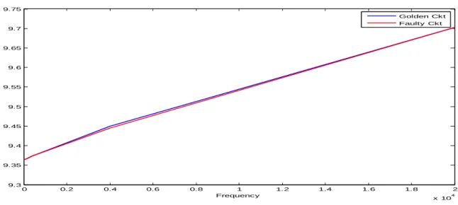
Assuming that, M1 is stuck open. Taking input bit 110, M2 and M4 will be connected with the virtual ground and M5 will be connected with the ground for both faulty and fault free circuit.
The equivalent circuit will be,
Fig 5.2: faulty circuit when M1 is stuck open
19 The input current of op-amp for the faulty circuit is 3𝐼
4
.
Similarly for the fault free circuit; we get the same input current of op-amp. As the current is same, we will get the same output voltage and gain for both faulty and fault free circuit. From the bellow graph, we can see that the gain error is negligible.
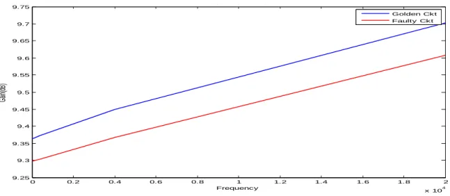
Fig 5.3: Gain Vs Frequency comparison between golden circuit and faulty circuit for M1 stuck open
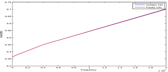
Fig 5.4: Gain Vs Frequency comparison between golden circuit and faulty circuit for M3 stuck open
0 0.2 0.4 0.6 0.8 1 1.2 1.4 1.6 1.8 2
x 104 9.3
9.35 9.4 9.45 9.5 9.55 9.6 9.65 9.7 9.75
Frequency
Gain(dB)
Gain Vs Frequency Comparison for :
Golden Ckt Faulty Ckt
0 0.2 0.4 0.6 0.8 1 1.2 1.4 1.6 1.8 2
x 104 9.3
9.35 9.4 9.45 9.5 9.55 9.6 9.65 9.7 9.75
Frequency
Gain(dB)
Gain Vs Frequency Comparison for :
Golden Ckt Faulty Ckt
20
Fig 5.5: Gain Vs Frequency comparison between golden circuit and faulty circuit for M5 stuck open
Fig 5.6: Gain Vs Frequency comparison between golden circuit and faulty circuit for M7 stuck open
Fig 5.7: Gain Vs Frequency comparison between golden circuit and faulty circuit for M9 stuck open
0 0.2 0.4 0.6 0.8 1 1.2 1.4 1.6 1.8 2
x 104 9.3
9.35 9.4 9.45 9.5 9.55 9.6 9.65 9.7 9.75
Frequency
Gain(dB)
Gain Vs Frequency Comparison for :
Golden Ckt Faulty Ckt
0 0.2 0.4 0.6 0.8 1 1.2 1.4 1.6 1.8 2
x 104 9.3
9.35 9.4 9.45 9.5 9.55 9.6 9.65 9.7 9.75
Frequency
Gain(dB)
Gain Vs Frequency Comparison for :
Golden Ckt Faulty Ckt
0 0.2 0.4 0.6 0.8 1 1.2 1.4 1.6 1.8 2
x 104 9.3
9.35 9.4 9.45 9.5 9.55 9.6 9.65 9.7 9.75
Frequency
Gain(dB)
Gain Vs Frequency Comparison for :
Golden Ckt Faulty Ckt
21
Fig 5.8: Gain Vs Frequency comparison between golden circuit and faulty circuit for M11 stuck open
Fig 5.9: Gain Vs Frequency comparison between golden circuit and faulty circuit for M13 stuck open
Fig 5.10: Gain Vs Frequency comparison between golden circuit and faulty circuit for M15 stuck open
0 0.2 0.4 0.6 0.8 1 1.2 1.4 1.6 1.8 2
x 104 9.3
9.35 9.4 9.45 9.5 9.55 9.6 9.65 9.7 9.75
Frequency
Gain(dB)
Gain Vs Frequency Comparison for :
Golden Ckt Faulty Ckt
0 0.2 0.4 0.6 0.8 1 1.2 1.4 1.6 1.8 2
x 104 9.3
9.35 9.4 9.45 9.5 9.55 9.6 9.65 9.7 9.75
Frequency
Gain(dB)
Gain Vs Frequency Comparison for :
Golden Ckt Faulty Ckt
0 0.2 0.4 0.6 0.8 1 1.2 1.4 1.6 1.8 2
x 104 9.3
9.35 9.4 9.45 9.5 9.55 9.6 9.65 9.7 9.75
Frequency
Gain(dB)
Gain Vs Frequency Comparison for :
Golden Ckt Faulty Ckt
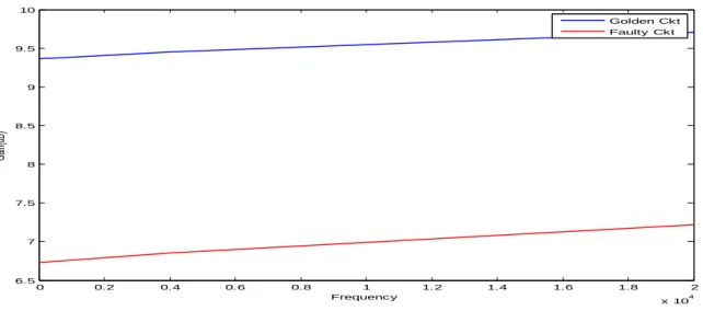
22 Table 5.2: Nmos faults(stuck open) in DAC
Fault Name RMS Error Gain(dB)
M2 stuck open 2.6001
M4 stuck open 0.24921
M6 stuck open 0.41807
M8 stuck open 0.4875
M10 stuck open 0.30599
M12stuck open 0.075207
M14 stuck open 0.63105
M16 stuck open 2.1976
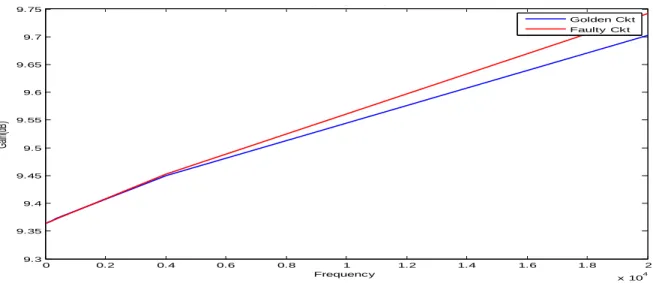
Comment:
Assuming that, M4 is stuck open. Taking input bit 011. As M4 is stuck opened in faulty circuit 2R resistance connected with M4 will be eliminated but in fault free circuit it will be connected with virtual ground. The equivalent circuit will be,
(a) (b) Fig 5.11(a): faulty circuit when M4 is stuck open;
(b): fault free circuit
23 The input current of op-amp for the faulty circuit is 𝐼
5
.
The input current of op-amp for the fault free circuit is 3𝐼8
.
Here, we can see that, the current of fault free circuit is greater than faulty circuit. So both output voltage & gain of fault free circuit will be greater than faulty circuit, which is shown in the following graph:
Fig5.12: Gain Vs Frequency comparison between golden circuit and faulty circuit for M2 stuck open
Fig 5.13: Gain Vs Frequency comparison between golden circuit and faulty circuit for M4 stuck open
0 0.2 0.4 0.6 0.8 1 1.2 1.4 1.6 1.8 2
x 104 6.5
7 7.5 8 8.5 9 9.5 10
Frequency
Gain(dB)
Gain Vs Frequency Comparison for :
Golden Ckt Faulty Ckt
0 0.2 0.4 0.6 0.8 1 1.2 1.4 1.6 1.8 2
x 104 9
9.1 9.2 9.3 9.4 9.5 9.6 9.7 9.8 9.9
Frequency
Gain(dB)
Gain Vs Frequency Comparison for :
Golden Ckt Faulty Ckt
24
Fig5.14: Gain Vs Frequency comparison between golden circuit and faulty circuit for M6 stuck open
Fig 5.15: Gain Vs Frequency comparison between golden circuit and faulty circuit for M8 stuck open
Fig 5.16: Gain Vs Frequency comparison between golden circuit and faulty circuit for M10 stuck open
0 0.2 0.4 0.6 0.8 1 1.2 1.4 1.6 1.8 2
x 104 9.3
9.4 9.5 9.6 9.7 9.8 9.9 10 10.1 10.2 10.3
Frequency
Gain(dB)
Gain Vs Frequency Comparison for :
Golden Ckt Faulty Ckt
0 0.2 0.4 0.6 0.8 1 1.2 1.4 1.6 1.8 2
x 104 9.3
9.4 9.5 9.6 9.7 9.8 9.9 10 10.1 10.2 10.3
Frequency
Gain(dB)
Gain Vs Frequency Comparison for :
Golden Ckt Faulty Ckt
0 0.2 0.4 0.6 0.8 1 1.2 1.4 1.6 1.8 2
x 104 9.3
9.4 9.5 9.6 9.7 9.8 9.9 10
Frequency
Gain(dB)
Gain Vs Frequency Comparison for :
Golden Ckt Faulty Ckt
25
Fig 5.17: Gain Vs Frequency comparison between golden circuit and faulty circuit for M12 stuck open
Fig 5.18: Gain Vs Frequency comparison between golden circuit and faulty circuit for M14 stuck open
Fig 5.19: Gain Vs Frequency comparison between golden circuit and faulty circuit for M16 stuck open
0 0.2 0.4 0.6 0.8 1 1.2 1.4 1.6 1.8 2
x 104 9.25
9.3 9.35 9.4 9.45 9.5 9.55 9.6 9.65 9.7 9.75
Frequency
Gain(dB)
Gain Vs Frequency Comparison for :
Golden Ckt Faulty Ckt
0 0.2 0.4 0.6 0.8 1 1.2 1.4 1.6 1.8 2
x 104 8.4
8.6 8.8 9 9.2 9.4 9.6 9.8
Frequency
Gain(dB)
Gain Vs Frequency Comparison for :
Golden Ckt Faulty Ckt
0 0.2 0.4 0.6 0.8 1 1.2 1.4 1.6 1.8 2
x 104 7
7.5 8 8.5 9 9.5 10
Frequency
Gain(dB)
Gain Vs Frequency Comparison for :
Golden Ckt Faulty Ckt
26 Table 5.3: Pmos faults(stuck on) in DAC
Fault Name RMS error,Gain(dB)
M1stuck on 2.6207
M3 stuck on 1.5787
M5 stuck on 1.2216
M7 stuck on 1.2857
M9 stuck on 1.7474
M11 stuck on 2.4029
M13 stuck on 3.5613
M15stuck on 8.1128
Comment:
Assuming that, M3 is stuck on. Taking input bit 011. As M3 is stuck oned, 2R resistance
connected with M3 will be connected with ground instead virtual ground of the am-opm in faulty circuit. The equivalent circuit will be,
(a) (b) Fig 5.20(a): faulty circuit when M3 is stuck on; (b): fault free circuit
27 The input current of op-amp for the faulty circuit is 𝐼
8
The input current of op-amp for the fault free circuit is 3𝐼
8
Here, we can see that, the current of fault free circuit is greater than faulty circuit. So both output voltage & gain of fault free circuit will be greater than faulty circuit, which is shown in the following graph:
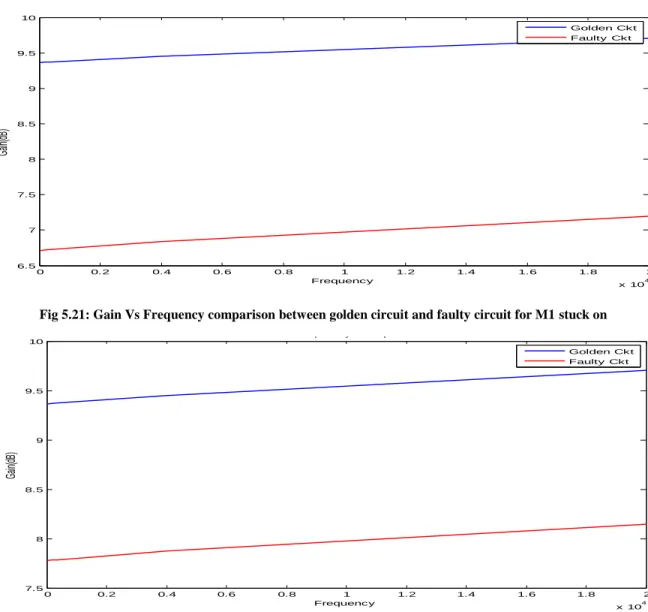
Fig 5.21: Gain Vs Frequency comparison between golden circuit and faulty circuit for M1 stuck on
Fig 5.22: Gain Vs Frequency comparison between golden circuit and faulty circuit for M3 stuck on
0 0.2 0.4 0.6 0.8 1 1.2 1.4 1.6 1.8 2
x 104 6.5
7 7.5 8 8.5 9 9.5 10
Frequency
Gain(dB)
Gain Vs Frequency Comparison for :
Golden Ckt Faulty Ckt
0 0.2 0.4 0.6 0.8 1 1.2 1.4 1.6 1.8 2
x 104 7.5
8 8.5 9 9.5 10
Frequency
Gain(dB)
Gain Vs Frequency Comparison for :
Golden Ckt Faulty Ckt
28
Fig 5.23: Gain Vs Frequency comparison between golden circuit and faulty circuit for M5 stuck on
Fig 5.24: Gain Vs Frequency comparison between golden circuit and faulty circuit for M7 stuck on
Fig 5.25: Gain Vs Frequency comparison between golden circuit and faulty circuit for M9 stuck on
0 0.2 0.4 0.6 0.8 1 1.2 1.4 1.6 1.8 2
x 104 8
8.2 8.4 8.6 8.8 9 9.2 9.4 9.6 9.8 10
Frequency
Gain(dB)
Gain Vs Frequency Comparison for :
Golden Ckt Faulty Ckt
0 0.2 0.4 0.6 0.8 1 1.2 1.4 1.6 1.8 2
x 104 8
8.2 8.4 8.6 8.8 9 9.2 9.4 9.6 9.8 10
Frequency
Gain(dB)
Gain Vs Frequency Comparison for :
Golden Ckt Faulty Ckt
0 0.2 0.4 0.6 0.8 1 1.2 1.4 1.6 1.8 2
x 104 7.5
8 8.5 9 9.5 10
Frequency
Gain(dB)
Gain Vs Frequency Comparison for :
Golden Ckt Faulty Ckt
29
Fig 5.26: Gain Vs Frequency comparison between golden circuit and faulty circuit for M11 stuck on
Fig 5.27: Gain Vs Frequency comparison between golden circuit and faulty circuit for M13 stuck on
Fig 5.28: Gain Vs Frequency comparison between golden circuit and faulty circuit for M15 stuck on
0 0.2 0.4 0.6 0.8 1 1.2 1.4 1.6 1.8 2
x 104 7
7.5 8 8.5 9 9.5 10
Frequency
Gain(dB)
Gain Vs Frequency Comparison for :
Golden Ckt Faulty Ckt
0 0.2 0.4 0.6 0.8 1 1.2 1.4 1.6 1.8 2
x 104 5
5.5 6 6.5 7 7.5 8 8.5 9 9.5 10
Frequency
Gain(dB)
Gain Vs Frequency Comparison for :
Golden Ckt Faulty Ckt
0 0.2 0.4 0.6 0.8 1 1.2 1.4 1.6 1.8 2
x 104 1
2 3 4 5 6 7 8 9 10
Frequency
Gain(dB)
Gain Vs Frequency Comparison for :
Golden Ckt Faulty Ckt
30 Table 5.4: Nmos faults(stuck on) in DAC
Fault Name RMS error, Gain(dB)
M2 stuck on 19.9954
M4 stuck on 15.0909
M6 stuck on 11.0337
M8 stuck on 7.8275
M10 stuck on 5.2082
M12 stuck on 3.1156
M14 stuck on 1.6319
M16 stuck on 0.028451
Comment:
Assuming that, M2 is stuck on. Taking input bit 011. As M2 is stuck oned, 2R resistance connected with M2 will be connected with virtual ground of the op-amp instead of ground. The equivalent circuit will be,
(a) (b) Fig 5.29 (a): faulty circuit when M2 is stuck on; (b): fault free circuit
31 The input current of op-amp for the faulty circuit is 7𝐼
8
The input current of op-amp for the fault free circuit is 3𝐼
8
Here, we can see that, the current of faulty circuit is greater than fault free circuit. So both output voltage & gain of faulty circuit will be greater than fault free circuit, which is shown in the following graph:
Fig 5.30: Gain Vs Frequency comparison between golden circuit and faulty circuit for M2 stuck on
Fig 5.31: Gain Vs Frequency comparison between golden circuit and faulty circuit for M4 stuck on
0 0.2 0.4 0.6 0.8 1 1.2 1.4 1.6 1.8 2
x 104 5
10 15 20 25 30
Frequency
Gain(dB)
Gain Vs Frequency Comparison for :
Golden Ckt Faulty Ckt
0 0.2 0.4 0.6 0.8 1 1.2 1.4 1.6 1.8 2
x 104 8
10 12 14 16 18 20 22 24 26
Frequency
Gain(dB)
Gain Vs Frequency Comparison for :
Golden Ckt Faulty Ckt
32
Fig 5.32: Gain Vs Frequency comparison between golden circuit and faulty circuit for M6 stuck on
Fig 5.33: Gain Vs Frequency comparison between golden circuit and faulty circuit for M8 stuck on
Fig 5.34: Gain Vs Frequency comparison between golden circuit and faulty circuit for M10 stuck on
0 0.2 0.4 0.6 0.8 1 1.2 1.4 1.6 1.8 2
x 104 8
10 12 14 16 18 20 22
Frequency
Gain(dB)
Gain Vs Frequency Comparison for :
Golden Ckt Faulty Ckt
0 0.2 0.4 0.6 0.8 1 1.2 1.4 1.6 1.8 2
x 104 9
10 11 12 13 14 15 16 17 18
Frequency
Gain(dB)
Gain Vs Frequency Comparison for :
Golden Ckt Faulty Ckt
0 0.2 0.4 0.6 0.8 1 1.2 1.4 1.6 1.8 2
x 104 9
10 11 12 13 14 15
Frequency
Gain(dB)
Gain Vs Frequency Comparison for :
Golden Ckt Faulty Ckt
33
Fig 5.35: Gain Vs Frequency comparison between golden circuit and faulty circuit for M12 stuck on
Fig 5.36: Gain Vs Frequency comparison between golden circuit and faulty circuit for M14 stuck on
Fig 5.37: Gain Vs Frequency comparison between golden circuit and faulty circuit for M16 stuck on
0 0.2 0.4 0.6 0.8 1 1.2 1.4 1.6 1.8 2
x 104 9
9.5 10 10.5 11 11.5 12 12.5 13
Frequency
Gain(dB)
Gain Vs Frequency Comparison for :
Golden Ckt Faulty Ckt
0 0.2 0.4 0.6 0.8 1 1.2 1.4 1.6 1.8 2
x 104 9.2
9.4 9.6 9.8 10 10.2 10.4 10.6 10.8 11 11.2
Frequency
Gain(dB)
Gain Vs Frequency Comparison for :
Golden Ckt Faulty Ckt
0 0.2 0.4 0.6 0.8 1 1.2 1.4 1.6 1.8 2
x 104 9.3
9.35 9.4 9.45 9.5 9.55 9.6 9.65 9.7 9.75 9.8
Frequency
Gain(dB)
Gain Vs Frequency Comparison for :
Golden Ckt Faulty Ckt
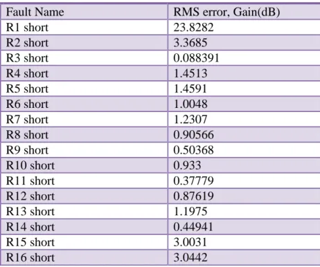
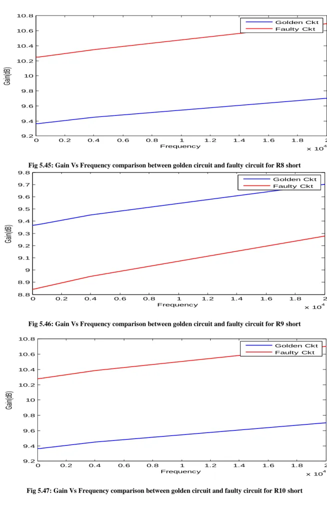
34 Table 5.5: Fault(short) in Resistance in DAC
Fault Name RMS error, Gain(dB)
R1 short 23.8282
R2 short 3.3685
R3 short 0.088391
R4 short 1.4513
R5 short 1.4591
R6 short 1.0048
R7 short 1.2307
R8 short 0.90566
R9 short 0.50368
R10 short 0.933
R11 short 0.37779
R12 short 0.87619
R13 short 1.1975
R14 short 0.44941
R15 short 3.0031
R16 short 3.0442
Comment:
For above faults, if any of the resistance is shorted, then the input current of op-amp in faulty circuit is expected to be greater than fault free circuit. So, both output voltage and gain of faulty circuit is expected to be greater than fault free circuit. This trend is observed in all faults
excepting R5, R7 & R9 short where a minor deviation is observed as shown in following graph,
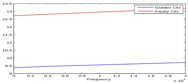
Fig 5.38: Gain Vs Frequency comparison between golden circuit and faulty circuit for R1 short
0 0.2 0.4 0.6 0.8 1 1.2 1.4 1.6 1.8 2
x 104 5
10 15 20 25 30 35
Frequency
Gain(dB)
Gain Vs Frequency Comparison for :
Golden Ckt Faulty Ckt
35
Fig 5.39: Gain Vs Frequency comparison between golden circuit and faulty circuit for R2 short
Fig 5.40: Gain Vs Frequency comparison between golden circuit and faulty circuit for R3 short
Fig 5.41: Gain Vs Frequency comparison between golden circuit and faulty circuit for R4 short
0 0.2 0.4 0.6 0.8 1 1.2 1.4 1.6 1.8 2
x 104 9
9.5 10 10.5 11 11.5 12 12.5 13 13.5
Frequency
Gain(dB)
Gain Vs Frequency Comparison for :
Golden Ckt Faulty Ckt
0 0.2 0.4 0.6 0.8 1 1.2 1.4 1.6 1.8 2
x 104 9.3
9.35 9.4 9.45 9.5 9.55 9.6 9.65 9.7 9.75
Frequency
Gain(dB)
Gain Vs Frequency Comparison for :
Golden Ckt Faulty Ckt
0 0.2 0.4 0.6 0.8 1 1.2 1.4 1.6 1.8 2
x 104 9
9.5 10 10.5 11 11.5
Frequency
Gain(dB)
Gain Vs Frequency Comparison for :
Golden Ckt Faulty Ckt
36
Fig 5.42: Gain Vs Frequency comparison between golden circuit and faulty circuit for R5 short
Fig 5.43: Gain Vs Frequency comparison between golden circuit and faulty circuit for R6 short
Fig 5.44: Gain Vs Frequency comparison between golden circuit and faulty circuit for R7 short
0 0.2 0.4 0.6 0.8 1 1.2 1.4 1.6 1.8 2
x 104 7.8
8 8.2 8.4 8.6 8.8 9 9.2 9.4 9.6 9.8
Frequency
Gain(dB)
Gain Vs Frequency Comparison for :
Golden Ckt Faulty Ckt
0 0.2 0.4 0.6 0.8 1 1.2 1.4 1.6 1.8 2
x 104 9.2
9.4 9.6 9.8 10 10.2 10.4 10.6 10.8
Frequency
Gain(dB)
Gain Vs Frequency Comparison for :
Golden Ckt Faulty Ckt
0 0.2 0.4 0.6 0.8 1 1.2 1.4 1.6 1.8 2
x 104 8
8.2 8.4 8.6 8.8 9 9.2 9.4 9.6 9.8 10
Frequency
Gain(dB)
Gain Vs Frequency Comparison for :
Golden Ckt Faulty Ckt
37
Fig 5.45: Gain Vs Frequency comparison between golden circuit and faulty circuit for R8 short
Fig 5.46: Gain Vs Frequency comparison between golden circuit and faulty circuit for R9 short
Fig 5.47: Gain Vs Frequency comparison between golden circuit and faulty circuit for R10 short
0 0.2 0.4 0.6 0.8 1 1.2 1.4 1.6 1.8 2
x 104 9.2
9.4 9.6 9.8 10 10.2 10.4 10.6 10.8
Frequency
Gain(dB)
Gain Vs Frequency Comparison for :
Golden Ckt Faulty Ckt
0 0.2 0.4 0.6 0.8 1 1.2 1.4 1.6 1.8 2
x 104 8.8
8.9 9 9.1 9.2 9.3 9.4 9.5 9.6 9.7 9.8
Frequency
Gain(dB)
Gain Vs Frequency Comparison for :
Golden Ckt Faulty Ckt
0 0.2 0.4 0.6 0.8 1 1.2 1.4 1.6 1.8 2
x 104 9.2
9.4 9.6 9.8 10 10.2 10.4 10.6 10.8
Frequency
Gain(dB)
Gain Vs Frequency Comparison for :
Golden Ckt Faulty Ckt
38
Fig 5.48: Gain Vs Frequency comparison between golden circuit and faulty circuit for R11 short
Fig 5.49: Gain Vs Frequency comparison between golden circuit and faulty circuit for R12 short
Fig 5.50: Gain Vs Frequency comparison between golden circuit and faulty circuit for R13 short
0 0.2 0.4 0.6 0.8 1 1.2 1.4 1.6 1.8 2
x 104 9.3
9.4 9.5 9.6 9.7 9.8 9.9 10 10.1 10.2 10.3
Frequency
Gain(dB)
Gain Vs Frequency Comparison for :
Golden Ckt Faulty Ckt
0 0.2 0.4 0.6 0.8 1 1.2 1.4 1.6 1.8 2
x 104 9.2
9.4 9.6 9.8 10 10.2 10.4 10.6 10.8
Frequency
Gain(dB)
Gain Vs Frequency Comparison for :
Golden Ckt Faulty Ckt
0 0.2 0.4 0.6 0.8 1 1.2 1.4 1.6 1.8 2
x 104 9.2
9.4 9.6 9.8 10 10.2 10.4 10.6 10.8 11 11.2
Frequency
Gain(dB)
Gain Vs Frequency Comparison for :
Golden Ckt Faulty Ckt
39
Fig 5.51: Gain Vs Frequency comparison between golden circuit and faulty circuit for R14 short
Fig 5.52: Gain Vs Frequency comparison between golden circuit and faulty circuit for R15 short
Fig 5.53: Gain Vs Frequency comparison between golden circuit and faulty circuit for R16 short
0 0.2 0.4 0.6 0.8 1 1.2 1.4 1.6 1.8 2
x 104 9.3
9.4 9.5 9.6 9.7 9.8 9.9 10 10.1 10.2
Frequency
Gain(dB)
Gain Vs Frequency Comparison for :
Golden Ckt Faulty Ckt
0 0.2 0.4 0.6 0.8 1 1.2 1.4 1.6 1.8 2
x 104 9
9.5 10 10.5 11 11.5 12 12.5
Frequency
Gain(dB)
Gain Vs Frequency Comparison for :
Golden Ckt Faulty Ckt
0 0.2 0.4 0.6 0.8 1 1.2 1.4 1.6 1.8 2
x 104 6
6.5 7 7.5 8 8.5 9 9.5 10
Frequency
Gain(dB)
Gain Vs Frequency Comparison for :
Golden Ckt Faulty Ckt
40 Table 5.6: Fault (stuck on) in Resistance & Capacitance across op-amp
Fault Name RMS error, Gain(dB)
r short 18.5537
C2 short 18.553
Comment:
When r & C2 are stuck oned, current doesn’t pass through the op-amp, so it cannot amplify. For this reason, both output voltage & gain of faulty circuit are less than fault free circuit as shown in graph,
Fig 5.54: Gain Vs Frequency comparison between golden circuit and faulty circuit for r short
Fig 5.55: Gain Vs Frequency comparison between golden circuit and faulty circuit for C2 short
0 0.2 0.4 0.6 0.8 1 1.2 1.4 1.6 1.8 2
x 104 -10
-8 -6 -4 -2 0 2 4 6 8 10
Frequency
Gain(dB)
Gain Vs Frequency Comparison for :
Golden Ckt Faulty Ckt
0 0.2 0.4 0.6 0.8 1 1.2 1.4 1.6 1.8 2
x 104 -10
-8 -6 -4 -2 0 2 4 6 8 10
Frequency
Gain(dB)
Gain Vs Frequency Comparison for :
Golden Ckt Faulty Ckt
41 Table 5.7: Fault (open) in Resistance & Capacitance in DAC
Fault Name RMS error, Gain(dB)
R1 open 2.6007
R2 open 10.5566
R3 open 0.24823
R4 open 6.631
R5 open 0.41945
R6 open 5.242
R7 open 0.48689
R8 open 4.6046
R9 open 0.30722
R10 open 4.0319
R11 open 0.092466
R12 open 3.133
R13 open 0.62976
R14 open 1.4569
R15 open 2.1973
R16 open 1.4254
Comment:
For above faults, if any of the resistance is stuck opened, then the input current of op-amp in faulty circuit is expected to be less than fault free circuit. So, both output voltage and gain of faulty circuit is expected to be less than fault free circuit. This trend is observed in all faults excepting R5,RR7 & R9 stuck open where a minor deviation is observed as shown in following graph,
Fig 5.56: Gain Vs Frequency comparison between golden circuit and faulty circuit for R1 open
0 0.2 0.4 0.6 0.8 1 1.2 1.4 1.6 1.8 2
x 104 6.5
7 7.5 8 8.5 9 9.5 10
Frequency
Gain(dB)
Gain Vs Frequency Comparison for :
Golden Ckt Faulty Ckt
42
Fig 5.57: Gain Vs Frequency comparison between golden circuit and faulty circuit for R2 open
Fig 5.58: Gain Vs Frequency comparison between golden circuit and faulty circuit for R3 open
Fig 5.59: Gain Vs Frequency comparison between golden circuit and faulty circuit for R4 open
0 0.2 0.4 0.6 0.8 1 1.2 1.4 1.6 1.8 2
x 104 -2
0 2 4 6 8 10
Frequency
Gain(dB)
Gain Vs Frequency Comparison for :
Golden Ckt Faulty Ckt
0 0.2 0.4 0.6 0.8 1 1.2 1.4 1.6 1.8 2
x 104 9.1
9.2 9.3 9.4 9.5 9.6 9.7 9.8
Frequency
Gain(dB)
Gain Vs Frequency Comparison for :
Golden Ckt Faulty Ckt
0 0.2 0.4 0.6 0.8 1 1.2 1.4 1.6 1.8 2
x 104 2
3 4 5 6 7 8 9 10
Frequency
Gain(dB)
Gain Vs Frequency Comparison for :
Golden Ckt Faulty Ckt

![CHAPTER 7 - introduction: PID controller design,” [Online]. Ava](data:image/gif;base64,R0lGODlhAQABAIAAAP///wAAACH5BAEAAAAALAAAAAABAAEAAAICRAEAOw==)