High Gain, Low Noise Cascode LNA with RF
Amplifier at 5.8GHz Using T-Matching Networks
Abu Bakar Ibrahim1, Abdul Rani Othman2, Mohd Nor Husain3, Mohammad Syahrir Johal4,
Abstract: This paper presents the high gain, low noise Cascode LNA with RF amplifier at 5.8GHz using T-matching network applicable for WIMAX application. The Cascode LNA uses FHX76LP Low Noise SuperHEMT FET and RF amplifier use EPA018A. The LNA designed used T-matching network consisting of lump element reactive element at the input and the output terminal. The Cascode LNA with RF amplifier produced gain of 35.5 dB and noise figure (NF) at 1.4 dB. The input reflection (S11) and output return loss (S22) are -12.4dB and -12.3 dB respectively. The bandwidth of the amplifier is more than 1.2 GHz. The input sensitivity is compliant with the IEEE 802.16 standards.
Keyword: Cascode LNA, RFA, T -Matching Network
I.INTRODUCTION
HE increasing number of personal wireless communication systems demand for Radio Frequency (RF) front-end capable to handle difference standard specification, i.e. WiMAX [1]. WiMAX, which is short for Worldwide Interoperability for Microwave Access, is a novel wireless communication technology. It is an attractive technology due to the high transmitting speed (up to 70Mbps) and long transmitting distance (up to 30 mile). The system bases on IEEE 802.16 standards and uses several bands (2.3-2.7 GHz, 3.4-3.6 GHz and 5.1-5.8GHz) to transmit data. The design of the front-end low noise amplifier (LNA) is one of the challenges in radio frequency (RF) receivers, which needs to provide good input impedance match, enough power gain and low noise figure (NF) within the required band [2].Many high gain amplifier topologies have been proposed as a way to satisfy the requirement for low power dissipation as well as good performances. The Cascode with RF amplifier to produces results in a higher bandwidth and gain, due to the increase in the output impedance, as well as better isolation between the input and output ports [3]. Most of the single stage LNA device in the review could only around 20 dB gain. It was proposed that the low noise amplifier should have a gain of at least 30 dB [8]. By taking consideration the extension of communication distance of up to 50 km [8]. A budgeted high gain of LNA will ensure a good signal to noise separation for further amplification.
Abu Bakar Ibrahim1, Abdul Rani Othman2, Mohd Nor Husain3, and
Mohammad Syahrir Johal4 are with the Faculty of Electronic and Computer Engineering, Universiti Teknikal Malaysia Melaka, Hang Tuah Jaya, 76100 Durian Tunggal, Melaka. Phone: +6065552128 Fax: +6065552112, Email: [email protected],[email protected],[email protected],sy [email protected].
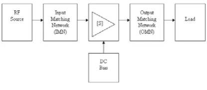
For this gain of 30 dB, a Cascode LNA with RF amplifier is introduced. It is shows in Fig.1.
Fig. 1 Cascode LNA and RFA
II.THEORETICAL ASPECTS
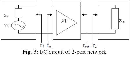
Basically, designing an amplifier, the input and output matching network are consider to achieve the required stability, small signal gain, and bandwidth. Super high frequency amplifier is a typical active circuit used to amplify the amplitude of RF signal. Basic concept and consideration in design of super high frequency amplifier is presented in this paper. The LNA designed, the formula and equation were referred to [4]. Figure 2, shows a typical single-stage amplifier including input/output matching networks.
Fig. 2 Typical amplifier design
The basic concept of high frequency amplifier design is to match input/output of a transistor at high frequencies using S-parameters frequency characteristics at a specific DC-bias point with source impedance and load impedance. Input/output matching circuit is essential to reduce the unwanted reflection of signal and to improve efficiency of the transmission from source to load [4], [5].
A. Power Gain
L L S IN
S
S
S
S
Γ
−
Γ
+
=
Γ
=
Γ
22 21 12 11 *1
S S L OUTS
S
S
S
Γ
−
Γ
+
=
Γ
=
Γ
11 21 12 22 *1
2 21 12 22 11 2 2 2 21 | ) ( ) 1 )( 1 ( | ) | | 1 )( | | 1 ( | | L S L S L S avs L T S S S S S P P source the from Available Power load the to delivered Power G Γ Γ − Γ − Γ − Γ − Γ − = = = 2 22 2 2 21 2|
1
|
|
|
1
|
|
|
|
1
1
supplied
L L in in L PS
S
P
P
amplifier
the
to
power
load
the
to
delivered
Power
G
Γ
−
Γ
−
Γ
−
=
=
=
3, power gains of 2-port circuit network with power impedance or load impedance at power amplifier represented with scattering coefficient are classified into Operating Power Gain, Transducer Power Gain and Available Power Gain [4],[5].
Fig. 3: I/O circuit of 2-port network
B. Operating Power Gain
Operating power gain is the ratio of power (PL) delivered
to the load (ZL) to power (Pin) supplied to 2-port network. Power delivered to the load is the difference between the power reflected at the output port and the input power, and power supplied to 2-port network is the difference between the input power at the input port and the reflected power. Therefore, Operating Power Gain is represented by
(1)
Where,
Γ
in indicates reflection coefficient of load at the inputport of 2-port network and
Γ
s is reflection coefficient of power supplied to the input port.C. Transducer Power Gain
Transducer Power Gain is the ratio of
P
avs , maximumpower available from source to
P
L, power delivered to the load. As maximum power is obtained when input impedance of circuit network is equal to conjugate complex number of power impedance, ifΓ
in =Γ
s , transducer power gain is represented by(2) Where,
Γ
L indicates load reflection coefficient.D. Available Power Gain
Available Power Gain,
G
Ais the ratio ofP
avs , poweravailable from the source, to
P
avn, power available from2-port network, that is,
avs avn A
P P
G = . Power gain is
P
avn whenin
Γ
=Γ
*
s. Therefore Available Power Gain is given by:(3)
That is, the above formula indicates power gain when input and output are matched [5].
E. Noise Figure
Signals and noises applied to the input port of amplifier were amplified by the gain of the amplifier and noise of amplifier itself is added to the output. Therefore, SNR (Signal to Noise Ratio) of the output port is smaller than that of the input port. The ratio of SNR of input port to that of output port is referred to as noise figure and is larger than 1 dB. Typically, noise figure of 2-port transistor has a minimum value at the specified admittance given by formula:
(4)
For low noise transistors, manufactures usually provide
opt N
Y
R
F
min,
,
by frequencies. N defined by formula for desired noise figure:(5)
F. Condition for Matching
The scattering coefficients of transistor were determined. The only flexibility permitted to the designer is the input/output matching circuit. The input circuit should match to the source and the output circuit should match to the load in order to deliver maximum power to the load. After stability of active device is demand, input/output matching circuits should be designed so that reflection coefficient of each port is correlated with conjugate complex number as given below [6]: (6) (7) 2 22 2 21 2 11 2 | 1 | 1 | | | 1 | | | 1 L S S avs avn A S S S P P source the from available Power amplifier the from available Power G Γ − Γ − Γ − = = = 2 min | s opt|
S N Y Y
G R F
F= + −
2 0 min 2 2 | 1 | / 4 | | 1 | | opt N S opt s Z R F F
N = − +Γ
Γ
−
Γ
+
=
Γ
=
Γ
s s out
L
S
S
S
S
11 21 12 22 *
1
The noise figure of the first stage of the receiver overrules noise figure of the whole system. To get minimum noise figure using transistor, power reflection coefficient should match with
Γ
opt and load reflection coefficient should matchwith
Γ
out*
Γ
s=Γ
opt (8)
(9)
III. CASCODE LNA AND RFADESIGN
Cascode LNA is designed based on the S-parameters were obtained from calculation and simulation using ADS 2008. The S-parameter for Cascode LNA is shows in Table I.
TABLE I:S-PARAMETERS OF CASCODE LNA
The overall performance of the low noise amplifier is determined by calculating the transducer gain GT, noise figure
F and the input and output standing wave ratios, VSWRIN and
VSWROUT. The optimum, Γopt and ΓL were obtained as Γopt = 17.949 + j48.881 and ΓL = 79.913-j7.304 for single
LNA.
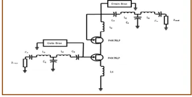
Fig. 4: The Schematic Circuit for Cascode LNA
Fig. 4 shows, the complete schematic circuit of 5.8 GHz a cascode Low noise amplifier. It is called inductive source degeneration. The passive elements in the input matching network are L1, L2 and C1.While; the passive elements in the
output matching network are L3, L4 and C2. The load
transistor consist of an inductor LD, it call peaking structure to
enhance gain and bandwidth [9]. This transistor also improves the reverse isolation and lowers miller effect [10],[13].
Fig. 5: The Schematic Circuit for RFA
Fig. 5 shows the completed schematic circuit of a RF amplifier with associated component and the 3 dB attenuator resistors. The RF amplifier was design based on [6] and [7]. Using theoretical design equation for the RFA, the equations are computed using Mathcad. The FET chosen for the design is EPA018A.The S-parameter given for the FET is shown in Table II. These parameter were measured at VDD =2V and
IDS= 10mA which sets the biasing for FET. This transistor
biasing circuit is similar with the LNA amplifier.
TABLE II :S-PARAMETERS OF RFAMPLIFIER
Gain, noise figure, input and output matching component were calculated and simulated using MathCAD and ADS 2008. Both calculated and simulated results were almost similar shows in Table IV. The calculated transducer power gain for matched condition was 17.3 dB. The input matching for optimum
Γ
optandL
Γ
were obtained asΓ
opt = 12.662 +j 38.168 andL
Γ
= 79.97- j7.286. The noise figure calculated is 2.475 dB. The RF amplifier can also act as an isolator for the overall front-end system and a suitable Π-network with 50Ώ load impedance was inserted at the input and output of the
amplifier to provide 3 dB attenuation each for the network. The purpose of 3 dB attenuation is to isolate the system from the reflected load power and to improve the return loss of overall systems. The Cascode LNA and RF amplifier Matching component are shown in Table III.
TABLE III:CASCODE LNA AND RFAMATCHING PARAMETERS Components LNA(Values) RFA(Values)
L1 6.14 nH 7.21nH
L2 2.4 nH 2.65nH
L3 1.55 nH 0.67nH
L4 1.62 nH 0.75nH
C1 0.315 pF 0.3pF
C2 429.9fF
IV. SIMULATION RESULT
Table IV is shows the S-parameters output for Cascode LNA, RF amplifier and Cascode LNA with RFA. It is simulated using Advanced Design System (ADS). The simulation recorded that the Cascode with RF amplifier gain S21 is 36.1 dB. The input insertion loss S11 is -12.14 dB,
overall noise figure (NF) is 1.3 dB and the output insertion loss S22 is -10.87 dB. The reflection loss S12 is -45.47 dB.
These values were within the design specification and were accepted. The outputs S-parameter are shown in Fig. 6a, 6b and 6c.
Frequency/dB S11 S12 S21 S22
5.8GHz 0.712 0.065 8.994 0.237
Angle -86.54 33.878 178.66 -10.456
Frequency/dB S11 S12 S21 S22
5.8 GHz 0.728 0.049 6.327 0.237
Fig. 6a: S-parametersfor Cascode
Fig. 6b: S-parametersfor RFA
Fig. 6c: S-parametersfor Cascode + RFA
TABLE IV:COMPARISON OF OUTPUT LNA
V. MEASUREMENT AND ANALYSIS
The result for Cascode LNA RF front-end was presented in
Table V.
TABLE V:SPARAMETER RESULT FOR CASCODE LNA
From the tabulated values, the S11 parameter measured is
11.5 dB. This is -1.5 dB less than targeted which is better and acceptable. S22 measured is -12.3 dB which is less than
targeted and acceptable. The return loss required S12 obtained
was less than -27.3 dB. The related measured gain S21 for the
LNA amplifier was 18.5 dB. The noise figure values obtained
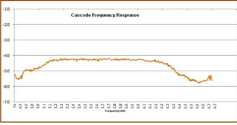
was 1.3 dB which complied with the targeted value of less 3 dB. The use of T lump reactive element and microstrip line matching technique at the input of the LNA contributes the best performance for the amplifier. This matching technique was used to provide high-loaded Q factor for better sensitivity and thus minimized the noise figure. The elements of T-network were realized in the form of lump reactive elements and microstrip line impedance. The 3 dB bandwidth for the amplifier is measured and the frequency response of LNA is shown in Fig. 7. The 3dB bandwidth obtained was 1.4 GHz compliant with targeted result of more than 1 GHz
The RF amplifier measurement setup was similar to the measurement set up for LNA. The results were shown in Table VI.
Fig. 7: Power output vs Frequency GHz Cascode LNA
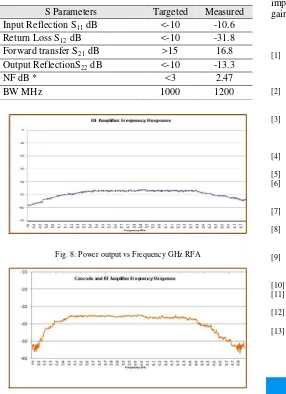
From the tabulated values, the S11 parameter measured is
-10.6 dB. This is -0.6 dB less than targeted which is better and acceptable. S22 measured is -13.3 dB which is less than
targeted and acceptable. The return loss required S12 obtained
is less than -31.8 dB which is also acceptable and better. The
use of Π-network with 50 Ώ load impedance at the input and
output of the RFA shows a better return loss which is lower than -31.8 dB.
The minimum return loss targeted for this amplifier is less than -10dB. The related measured gain S21 for the RF
amplifier is 16.8 dB measured. The noise figure values obtained is 2.47 dB which complied with the targeted value of 3dB. Again shows that the use of T lump reactive element and microstrip matching network provide best performance for the RF Amplifier since the measure value nearly optimized. The 3dB bandwidth obtained is 1200 MHz which is more than the targeted result of 1GHz.
Both amplifiers were then cascaded and tested with 10dB attenuation set on the spectrum analyzer the output power versus frequency is shown in Fig. 9. It was observed that the power output is -36.5 dBm and is expected if includes the total loss from cable and connector of 2 dB.
The Front-end system designed consisted of a LNA with RFA were developed. The final result for overall amplifier gain is 35.5 dB gains with noise figure of 1.3 dB. The total insertion loss is -25.5 dB. With injecting a -60 dBm signal and that attenuator setup of spectrum is 10 dB.
S-Parameters
(dB) S11 S12 S21 S22 NF
Cascode LNA -18.9 -22.1 19.5 -20.0 1.2 RF Amplifier -12.5 -21.5 17.3 -12.6 2.40
Cascode and
RFA -24.3 -62.6 36.1 -23.86 1.30
S Parameters Targeted Measured
Input Reflection S11 dB <-10 dB -11.5
Return Loss S12 dB <-10 dB -27.3
Forward transfer S21 dB >17 dB 18.5
Output ReflectionS22 dB <-10 dB -12.3
NF dB * <3 dB 1.3
Table VI: S-Parameters for RF Amplifier
Fig. 8: Power output vs Frequency GHz RFA
Fig. 9: Power output vs Frequency for Cascode LNA + RF Amp
For a wireless communication system such as WiMAX system, this RF front-end receiver will capable to provide a better pipeline for the receiver with minimum noise figure and provide a high gain. This output is acceptable for further processing of the baseband system for IEEE 802.16 WiMAX standard.
VI. CONCLUSION
The Cascode LNA with RFA has been simulated and developed successfully with IEEE standard 802.16 WiMAX. It is observed that the simulated and experiment results have not much different. It observed that the gain of the simulated analysis is 36.1 dB and the experimental value is 35.5 dB while; the noise figure (NF) measured is less than 1.4 dB. It is important to take note when designing the amplifier to match the amplifier circuits. The Cascode LNA with RF Amplifier has been developed successfully and the circuit cab contributed to the front end receiver at the described
frequency. For better performance in gain of the amplifier, it can be achieved by increasing the number of stages to improve the gain and noise figure of the design [11]. Higher gain would expand the coverage or communication distance.
REFERENCES
[1] Edwin C, Becerra Alvarez, Jose M.de la Rose and Federico Sandoval. “ Design of a 1V 90-nm CMOS Folded Cascode LNA for Multi-Standerd Application”. IEEE Proceeding 2010.
[2] Ruey-Lue Wang, Shih-Chih Chen, Cheng-Lin Huang, Chien-Hsuan Lie,Yi-Shu Lin. "2-6GHz Current-Reused LNA With Transformer-type Inductors." IEEE Proceeding 2008.
[3] Leon, Michael Angelo G.Lorenzo and Maria Theresa G.De. "Comparison of LNA Topology for Wimax Application in a Standard 90-nm CMOS Process." 12th International Conference on Computer Modelling and Simulation. 2010. pp-642-647. [4] M.Pozar, David. Microwave and RF Wireless System. Third
Avenue, N.Y.John Wiley & Sons, in 2001.
[5] Gonzalez, Guillermo. Microwave Transistor Amplifier. 1996. [6] Garuda C.& Mohammad,I. ‘A Multi Band CMOS RF Rront-End
for 4G Wimax & WLAN Application.IEEE Transection on Microwave Theory & Techniques, pp 3049-3052. 2006
[7] M.Pozar, David. Microwave and Engineering. N.Y.John Wiley & Sons, in 2005.
[8] IEEE Computer Society and IEEE Microwave Theory Technique and Society. Part 16 Air Interface For Fix Broadband Wireless System, IEEE Standard 802.16. 2004
[9] Dorra Ayadi, Saul Rodriguez, Mourad Loulou, and Mohammad Ismail. “ System Level Design of Radio Frequency Receiver for IEEE 802.16 Standard”. IEEE Proceeding 2009.
[10] Richard Chi-His Li. RF Circuit Design, 2009
[11] Inder J.Bahl. Fundamentals of RF and Microwave Transistor Amplifier. 2009
[12] Bhartia, P. & Bahl, I. Microwave Solid State Circuit Design, 2nd
Edition, J Wiley, 2003.
[13] A.Baishya, P. P.Sahu and M.K.Naskar. A High Gain Low Noise Amplifier for 0.9 – 6GHz Wireless Application. IEEE Proceeding, 2011
Abu Bakar Ibrahim received the B.S degree in
electrical engineering and master degree from University of Technology Malaysia in 1998 and 2000 respectively. Currently is working toward the Ph.D. degree in development of low noise amplifier front-end receiver for wireless application at the Universiti Teknikal Malaysia Melaka.
Email: [email protected]
Abdul Rani Othman received B.eng in
electrical and Electronic from University of Strathclyde and master degree in electrical and electronic from University Technology of Malaysia. He received Ph.D. in RF front-end receiver for wireless application from University of Teknikal Malaysia Melaka and now he joined Universiti Teknikal Malaysia Melaka. Email: [email protected]
Mohd Nor Husain received B.S in electrical and
Electronic Engineering from University of Strathclyde and master degree in electronic communication from University of Essex England. He received Ph.D. in optical and waveguide from University of Bath England and now he joined Universiti Teknikal Malaysia Melaka. Email:[email protected]
S Parameters Targeted Measured
Input Reflection S11 dB <-10 -10.6
Return Loss S12 dB <-10 -31.8
Forward transfer S21 dB >15 16.8
Output ReflectionS22 dB <-10 -13.3
NF dB * <3 2.47