DOI: 10.12928/TELKOMNIKA.v14i2A.4359 138
Circuit Simulation for Bridge Ignition Feature of
Semiconductor
Mingfang Liu*, Lin Yu, Xia Han
School of Electrical and Photoelectronic Engineering, Changzhou Institute of Technology, Changzhou, Jiangsu, 213002, China
*Corresponding author, email: summerlmf@126.com
Abstract
The emergence of ignition device of semiconductor bridge provides a way to resolve the conflict between low energy and high promptness, reliability and safety of initiating explosive device. But with the rapid development of arms and ammunition, the higher demand of miniaturization for structure and volume in design of initiating explosive device is put forward based on high safety, reliability and promptness and low ignition energy. The heat dissipation effect of all structural parts is assessed, the measures to optimize the structure are put forward, the numerical simulation is adopted for simulation and the accuracy of optimization design plan is finally physically verified in the Thesis based on thermal analysis of ignition device of semiconductor bridge in maximum no-fire test. The finite-element numerical simulation analysis provides theoretical basis and comparison and assessment of various plans in optimization design for ignition device of semiconductor bridge, and greatly shortens the time and reduces the design errors in optimization design for ignition device of semiconductor bridge; meanwhile, it assists in product development and design as the platform for design, analysis and verification.
Keywords: Semiconductor bridge; Ignition device; Ignition energy; Reliability; Miniaturization
1. Introduction
The current ignition part for igniter of domestic industrial electric detonator is composed of electric heating bridge wire and agent; during the fabrication of bridge wire and preparation of agent, caused by raw materials, production technology, etc., the consistency of resistance and agent sensitivity is poor, so the agent will easily cause malfunction under the action of relatively high static electricity and electromagnetic radiation which can result in unsafe problems during production, storage, transportation and use. As the rapid development of the modern society, the radiation and interference caused by static electricity, stray current, electromagnetic wave, etc. are more and more intensive and the environment is becoming more and more complicated, so the demand for the ability of static electricity, stray current and anti-electromagnetic wave of industrial electric detonator during production, storage, transportation and use is increasingly high [1-5]. Because the resistance of semiconductor detonator in normal temperature is relatively high, the safety performance for ignition device of semiconductor bridge in static electricity, stray current and electromagnetic radiation is much better and the safety performance of product can be substantially raised for semiconductor detonator combined with detonator.
2. Structure and Operation Principle of Semiconductor Bridge
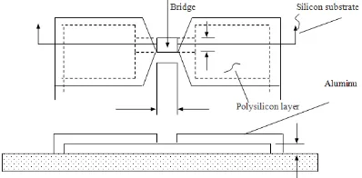
Figure 1. Chip structure of semiconductor bridge
In Figure 1, the module of semiconductor bridge is composed of silicon/heavy doping area from front view, the depth (D) of bridge is determined by the geometric dimension of the doped thin polysilicon layer and the length (L) and width (W) of bridge are determined by the geometric structure of electrode for thin aluminum layer.
When the rapidly rising current pulse is imposed on the electrodes at both ends of semiconductor bridge, the current will produce glow discharge along the bridge edge with the maximum current gradient and excite towards the bridge centre; due to the inherent negative resistivity for materials in bridge area, the bridge area with larger current can greatly intensify the excitation effect with a view to accelerating material melting in semiconductor bridge area, forming superthermal ionized steam layer and producing strong plasma glow discharge gas; when the glowing silicon plasma passes through the neighbouring powdered explosive, it condenses on the explosive particle for heat exchange, then the explosive is ignited and explosion occurs.
3. Design for Ignition Device of Semiconductor Bridge
Figure 2. Geometric model for ignition device of semiconductor bridge
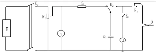
The dimension of semiconductor bridge is closely related to the ignition energy for initiating explosive device of semiconductor; in case the dimension of bridge is oversized, the energy added to the bridge cannot vaporize the silicon, so it is hard to make the initiating explosive device act; if the dimension of bridge is undersized, the silicon content for plasma resulting from evaporation is small, so the clinical ignition amount of initiating explosive device cannot be achieved. When the energy supplied to the semiconductor is relatively less, the semiconductor bridge cannot generate a burst of plasma and the bridge area will instantly fuse off. When the energy for semiconductor bridge area is slowly supplied, the bridge area will gradually become hot and spark state will occur with the increase of current; finally the bridge area will fuse off and the plasma cannot be generated. Only when the sufficient energy is supplied to the bridge area, the bridge area can generate plasma. The lifting and lowering test method for capacitor discharge device of detonator in WJ/T9039-2004 standard Test Method for Ignition Pulse Energy of Industrial Electric Detonator is adopted to find the distance from ignition voltage and semiconductor bridge to fire hole. The schematic diagram for lifting and lowering test device is shown in Figure 3.
Figure 3. Test device for capacitor discharge
The test analysis is as follows:
Table 1. (Each group containing 50 detonators)
Group
Item Distance from semiconductor
bridge to fire hole
Minimum ignition voltage
Maximum non-ignited voltage
Maximum ignition pulse energy
1 5mm-7mm 135V 60V 37mjΩ-1
2 4mm-5mm 110V 60V 25mjΩ-1
3 3mm
Below 3mm 90V 45V 13mjΩ
3 3mm
Below 3mm 90V 45V 12mjΩ
-1
As shown in the test results, the farther the distance from semiconductor bridge to fire hole, the greater the energy required by semiconductor bridge. The structure and shape for ignition device of semiconductor bridge are shown in Figure 4. The ignition device of semiconductor bridge is mainly composed of semiconductor bridge, electrode plug, metal shell, pouring sealant, initiating explosive, ignition agent, etc. The semiconductor bridge is fabricated by semiconductor bridge chip; it is the ignition element for ignition device of semiconductor bridge is composed of silicon slice, silicon bridge film, aluminum-coated electrode or gold-coated electrode; it conforms to the following requirements: 1. the thickness of silicon slice cannot exceed 0.5mm; 2. the phosphorus-doped polysilicon is deposited on the silicon slice through low-pressure chemical vapor deposition method for silicon bridge film; 3. the gold-coated electrode on silicon bridge film is deposited into thin film through vacuum coating and the is fabricated through photoetching method according to the required shape and dimension; 4. the silicon bridge film and electrode shall be checked by the magnifier not greater than 80 times and the graph is clean and complete without burr at the edge and puncture, pinhole, bulge, spot, grease stain or foreign matter. The electrode plug is composed of glass with relatively high compactness. For electrical connection of semiconductor bridge chip and electrode plug, first stick the chip on the prescribed position of electrode plug with binder; then adopt the gold ball bonding method to conduct redundancy welding for gold wire and the electrode of electrode plug with three lead wires for each electrode welding. The energy conversion element for ignition device of semiconductor bridge is semiconductor bridge and the ignition mechanism is plasma microconvection mechanism of action. When the system sends the ignition signal, the capacitor discharge generates rapid electric pulse and the semiconductor bridge generates thermal ions to detonate the initiating explosive and output flame energy.
4.Results and Analysis 4.1. Rapid Ignition Speed
The mechanism of action for semiconductor ignition is microconvection. When the semiconductor bridge is supplied with pulse current, the rapidly vaporized silicon bridge material due to joule heat will form the weak plasma to discharge under the action of electric field, the plasma will rapidly spread to the initiating explosive in the detonator to transfer the heat to the initiating explosive in extremely rapid speed with a view to making the explosive explode when the explosive reaches the combustion temperature; in addition, the rapid spread of plasma can generate impulse wave to impact the initiating explosive and make it explode. The mechanism of action for bridge wire is thermal conduction; because the action speed of convection and impact is much faster than that of thermal conduction, so the characteristic of the bridge wire is that acts faster than fast traditional bridge wire and it provides good conditions for prompt detonator. The time from power supply to detonation for semiconductor detonator is tested as shown in Table 3.
Table 3. (20 test samples)
Test device Rapid initiation switch, detonation speed tester and protection device. Time from power supply to detonation μs
775 720 789 821 810 743 815 779 753 859
824 798 806 827 816 810 759 792 851 853
As shown above, it is indicated that the time for semiconductor bridge detonator is within 1ms. According to the previous analysis, in the maximum non-ignited energy test for ignition device of semiconductor bridge (according to GJB344A-2005 General Design Code for Insensitive Electric Initiator), the energy input to the semiconductor bridge is larger than that for ignition device of semiconductor bridge lost around and when the temperature of semiconductor bridge rises as the accumulation of heat and reaches the temperature at bursting point of 5s for lead styphnate, the lead styphnate explodes. The following conclusions are drawn from thermal conduction of interface: 1. the heat generated by semiconductor bridge cannot be promptly conducted away; 2. the heat dissipation function of electrode plug is insufficient.
4.2. Excellent Anti-Static Electricity, Anti-Electromagnetic Radiation and Anti-Stray Current Performance of Semiconductor Bridge
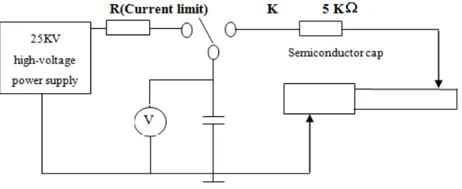
The basic circuit diagram for electrostatic sensitivity is shown in Figure 5.
25KV
Anti-electromagnetic radiation test, test items and equipment (1) Test items: RS103——10KHZ-1GKHZ
Test equipment: 500W power amplifier PA1, 150W power amplifier PA2, field intensity indicator FM5004, field intensity probe FP5000, signal source SMY and power meter NRVD
(2) Test items: RS103——1G KHZ-18GKHZ
Test equipment: 200W power amplifier PA3, 200W power amplifier PA4, field intensity indicator FM5004, field intensity probe FP5080, signal source SMR20 and power meter NRVD1 and NRVD2
(3) Test items: RS101——25HZ-100KHZ
Test equipment: signal source HP33102A, receiver ES126, current probe EZ-17 radiation ring and audio frequency amplifier BRYSTON.
Table 5. Test conclusions
Group Item
Radiosensitivity of electric field Test results Remarks
1 RS103——10KH- 1GKHZ Stable performance without explosion
2 RS103——1GKH-18GKHZ Stable performance without explosion
3 RS101——25HZ-100KHZ Stable performance without explosion
After the test, the product can satisfy multiple standard requirements of RE101, R102 and RS103; the product does not explode in the continuous frequency scope of 10KHZ-18GHZ and the strong radiation intensity of 200 V/m.
5. Conclusion
Through the above research results, simulation calculation and experimental verification, there are four conclusions and the main contradictions are determined. Analyze and demonstrate the four conclusions and obtain the optimization plan according to the design requirements for ignition device of semiconductor bridge. According to the design requirements for igniting explosive device of semiconductor bridge, the promptness and reliability of action will be improved; the lead styphnate is generally adopted for current agent design and polysilicon doping design is adopted for semiconductor bridge. So the optimization design for ignition device of semiconductor bridge refers to optimization and improvement of electrode plug. Therefore, the following measures are put forth: 1. change the material of electrode plug and replace the glass material with 95%Al2O3 insulation ceramics; 2 redesign the structure of electric
plug and insert the semiconductor bridge into the electrode plug.
Acknowledgements
References
[1] Yan X, Wu Q, Zhang C, Li W, Chen W, Luo W. An improved genetic algorithm and its application. Indonesian Journal of Electrical Engineering and Computer Science. 2012; 10(5): 1081-1086. [2] Lv Z, Halawani A, Feng S. Multimodal hand and foot gesture interaction for handheld devices. ACM
Transactions on Multimedia Computing, Communications, and Applications (TOMM). 2014; 11(1s): 10.
[3] Tie Wang, Chao Wang, Jing Wu. Accord Ignition Diagnosis Based on Improved GABP.
TELKOMNIKA Indonesian Journal of Electrical Engineering. 2014; 12(2): 1367-1373.
[4] Guanxiong Liu, Yishuang Geng, Kaveh Pahlavan. Effects of calibration RFID tags on performance of inertial navigation in indoor environment. Networking and Communications. 2015.
[5] A Triwiyatno. Engine Torque Control of Spark Ignition Engine using Fuzzy Gain Scheduling. TELKOMNIKA Indonesian Journal of Electrical Engineering. 2012; 10(1): 83-90.
[6] Wenhua Huang, Yishuang Geng. Identification Method of Attack Path Based on Immune Intrusion Detection, Journal of Networks. 2014; 9(4): 964-971.
[7] Jie He, Yishuang Geng, Fei Liu, Cheng Xu. CC-KF: Enhanced TOA Performance in Multipath and NLOS Indoor Extreme Environment. IEEE Sensor Journal. 2014; 14(11): 3766-3774.
[8] A Sujono, R Soekrisno, E Firmansyah, O Wahyunggoro. Power Optimization of Spark Ignition Engine by Fuzzy Logic Ignition Controller Based on Knock Detection. TELKOMNIKA Indonesian Journal of Electrical Engineering. 2015; 14(2): 280-287.
[9] Na Lu, Caiwu Lu, Zhen Yang, Yishuang Geng. Modeling Framework for Mining Lifecycle
Management. Journal of Networks. 2014; 9(3): 719-725.
[10] Yishuang Geng, Kaveh Pahlavan. On the accuracy of rf and image processing based hybrid localization for wireless capsule endoscopy. IEEE Wireless Communications and Networking Conference (WCNC). 2015.