COMBINATIONAL LOGIC
FUNCTIONS
Contents
9.1 9.2 9.3 9.4 9.5 9.6 9.7 9.8Introduction . . . .
A Half-Adder . . . .
A Full-Adder . . . .
Decoder . . . .
Encoder . . . .
Demultiplexers . . . .
Multiplexers . . . .
Using multiple combinational circuits
. . . . . . . . . . . . . . . . . . . . . . . . . . . . . . . . . . . . . . . . . . . . . . . . . . . . . . . . . . . . . . . . . . . . . . . . . . . . . . . . . . . . . . . . . . . . . . . . . . . . . . . . . . . . . . . . . . . . . . . . . . . . . . . . . . . . . . . . . . . . . . . . . . . . . . . . . . . . . . . . . . . . . . . . 273 274 275 282 286 289 293 294
Original author: David Zitzelsberger
9.1
Introduction
The term ”combinational” comes to us from mathematics. In mathematics a combination is an unordered set, which is a formal way to say that nobody cares which order the items came in. Most games work this way, if you rolled dice one at a time and get a 2 followed by a 3 it is the same as if you had rolled a 3 followed by a 2. With combinational logic, the circuit produces the same output regardless of the order the inputs are changed.
There are circuits which depend on the when the inputs change, these circuits are called sequential logic. Even though you will not find the term ”sequential logic” in the chapter titles, the next several chapters will discuss sequential logic.
Practical circuits will have a mix of combinational and sequential logic, with sequential logic making sure everything happens in order and combinational logic performing functions like arithmetic, logic, or conversion.
274 CHAPTER 9. COMBINATIONAL LOGIC FUNCTIONS
You have already used combinational circuits. Each logic gate discussed previously is a combinational logic function. Lets follow how two NAND gate works if we provide them inputs in different orders.
We begin with both inputs being 0.
00
1
1
We then set one input high.
10
1
1
We then set the other input high.
11
0
0
So NAND gates do not care about the order of the inputs, and you will find the same true of all the other gates covered up to this point (AND, XOR, OR, NOR, XNOR, and NOT).
9.2
A Half-Adder
9.3. A FULL-ADDER 275
0+0=00+1=11+0=11 + 1 = 102
So we well need two inputs (a and b) and two outputs. The low order output will be called because it represents the sum, and the high order output will be called C out because it represents the carry out.
The truth table is
A
0
0
1
1
B
0
1
0
1
C
out00
10
10
01
Simplifying boolean equations or making some Karnaugh map will produce the same circuit shown below, but start by looking at the results. The column is our familiar XOR gate, while the Cout column is the AND gate. This device is called a half-adder for reasons that will make sense in the next section.
A
B
C
outor in ladder logic
L
1A
A
A
B
B
B
C
out
L
29.3
A Full-Adder
276 CHAPTER 9. COMBINATIONAL LOGIC FUNCTIONS
make a four digit adder, do it again. Then when ... The circuits would be fast, but development time would be slow.
Looking at a two binary digit sum shows what we need to extend addition to multiple binary digits.
11
11 11 110
Look at how many inputs the middle column uses. Our adder needs three inputs; a, b, and the carry from the previous sum, and we can use our two-input adder to build a three input adder.
is the easy part. Normal arithmetic tells us that if = a + b + Cin and 1 = a + b, then = 1 + Cin .
A
B
C
inL
1A
A
A
1
1
1
1HA
C
1
HA
C
2L
2B
B
B
C
inC
inC
in
1C
1
C
2What do we do with C1 and C2 ? Let’s look at three input sums and quickly calculate:
Cin + a + b = ?
0+0+0=00+0+1= 10+1+0= 1
9.3. A FULL-ADDER
1+0+0=1 1 + 1 = 11
1 + 0 + 1 = 10 1 + 1 + 0 = 10
277
1+
If you have any concern about the low order bit, please confirm that the circuit and ladder calculate it correctly.
In order to calculate the high order bit, notice that it is 1 in both cases when a + b produces a C1 . Also, the high order bit is 1 when a + b produces a 1 and Cin is a 1. So We will have a carry when C1 OR ( 1 AND Cin ). Our complete three input adder is:
A
B
C
inHA
1HA
C
outL
1A
A
A
1
1
1C
1B
B
B
C
inC
inC
inC
2C
2C
outC
1
1L
2For some designs, being able to eliminate one or more types of gates can be important, and you can replace the final OR gate with an XOR gate without changing the results.
278 CHAPTER 9. COMBINATIONAL LOGIC FUNCTIONS
A
0B
0HA
A
1B
1L
1A
0A
0A
0A
1A
1A
1T
1T
1T
1TC
1B
0B
0B
0B
1B
1B
1C
1C
1C
1TP
1
0
1FA
C
out
L
2
0C
1T
1TC
1
1TP
1C
outA0 is the low order bit of A, A1 is the high order bit of A, B0 is the low order bit of B, B1 is the high order bit of B, 0 is the low order bit of the sum, 1 is the high order bit of the sum, and Cout is the Carry.
9.3. A FULL-ADDER 279
C
inA
0B
0FA
A
1B
1
1FA
C
out
280 CHAPTER 9. COMBINATIONAL LOGIC FUNCTIONS
L1
A0
A0
A0
T 0
T 0
TC0
TC0
A1
A1
A1
T 1
T 1
T 1
TC1
B0
B0
B0
Cin
Cin
Cin
TP0
B1
B1
B1
C1
C1
C1
TP1
TP1
Cout
TC1
1
TP0
C1
T 1
TC0
0
T 0
L2
There are several reasons for this, one being that we can then allow a circuit to determine whether the lowest order carry should be included in the sum. This allows for the chaining of even larger sums. Consider two different ways to look at a four bit sum.
1111<-+
9.3. A FULL-ADDER 281
| | 100011 +-100 +-101
If we allow the program to add a two bit number and remember the carry for later, then use that carry in the next sum the program can add any number of bits the user wants even though we have only provided a two-bit adder. Small PLCs can also be chained together for larger numbers.
These full adders can also can be expanded to any number of bits space allows. As an example, here’s how to do an 8 bit adder.
0FA
C
in
1FA
2FA
3FA
4FA
5FA
6FA
7C
outFA
A
7B
77 Cout
2+
A7 B7
FA
A
0B
0A
1B
1A
2B
2A
3B
3A
4B
4A
5B
5A
6B
6This is the same result as using the two 2-bit adders to make a 4-bit adder and then us-ing two 4-bit adders to make an 8-bit adder or re-duplicatus-ing ladder logic and updatus-ing the numbers.
0 1 2 3 4 5 6
FA FA FA FA FA FA
Cin
2+
4+
A0 B0 A1 B1 A2 B2
2+
A3 B3 A4 B4
2+
4+
A5 B5 A6 B6
Each ”2+” is a 2-bit adder and made of two full adders. Each ”4+” is a 4-bit adder and made of two 2-bit adders. And the result of two 4-bit adders is the same 8-bit adder we used full adders to build.
For any large combinational circuit there are generally two approaches to design: you can take simpler circuits and replicate them; or you can design the complex circuit as a complete device.
Using simpler circuits to build complex circuits allows a you to spend less time designing but then requires more time for signals to propagate through the transistors. The 8-bit adder design above has to wait for all the Cxout signals to move from A0 + B0 up to the inputs of 7 . If a designer builds an 8-bit adder as a complete device simplified to a sum of products, then each signal just travels through one NOT gate, one AND gate and one OR gate. A seventeen input device has a truth table with 131,072 entries, and reducing 131,072 entries to a sum of products will take some time.
When designing for systems that have a maximum allowed response time to provide the final result, you can begin by using simpler circuits and then attempt to replace portions of the circuit that are too slow. That way you spend most of your time on the portions of a circuit that matter.
282 CHAPTER 9. COMBINATIONAL LOGIC FUNCTIONS
9.4
Decoder
A decoder is a circuit that changes a code into a set of signals. It is called a decoder because it does the reverse of encoding, but we will begin our study of encoders and decoders with decoders because they are simpler to design.
A common type of decoder is the line decoder which takes an n-digit binary number and decodes it into 2n data lines. The simplest is the 1-to-2 line decoder. The truth table is
A D
1D
0001
11 0
A is the address and D is the dataline. D0 is NOT A and D1 is A. The circuit looks like
A
D
0D
1L
1A
A
D
0D
1L
2Only slightly more complex is the 2-to-4 line decoder. The truth table is
A
1A
000
01
10
11
D
30
0
0
1
D
20
0
1
0
D
10
1
0
0
D
01
0
0
0
9.4. DECODER 283
A
0A
1D
0D
1D
2D
3L
1A
1A
1A
1A
1A
0A
0A
0A
0D
0D
1D
2D
3L
2284 CHAPTER 9. COMBINATIONAL LOGIC FUNCTIONS
D
0A
0A
11-to-2
Decoder
1-to-2
Decoder
D
1D
2D
3Replacing the 1-to-2 Decoders with their circuits will show that both circuits are equivalent. In a similar fashion a 3-to-8 line decoder can be made from a 1-to-2 line decoder and a 2-to-4 line decoder, and a 4-to-16 line decoder can be made from two 2-to-4 line decoders.
9.4. DECODER 285
L
1A
0A
0A
1A
1T
1,0T
1,0T
1,1T
1,1T
0,0T
0,1T
0,0T
0,1T
0,0T
0,1T
1,0T
1,1D
0D
1D
2D
3L
2For some logic it may be required to build up logic like this. For an eight-bit adder we only know how to sum eight bits by summing one bit at a time. Usually it is easier to design ladder logic from boolean equations or truth tables rather than design logic gates and then ”translate” that into ladder logic.
286 CHAPTER 9. COMBINATIONAL LOGIC FUNCTIONS
9.5
Encoder
An encoder is a circuit that changes a set of signals into a code. Lets begin making a 2-to-1 line encoder truth table by reversing the 1-to-2 decoder truth table.
D
1D
0A
0
1
10
01
table.
This truth table is a little short. A complete truth table would be
D
10
0
1
1
D
0A
0
10
01
1
One question we need to answer is what to do with those other inputs? Do we ignore them? Do we have them generate an additional error output? In many circuits this problem is solved by adding sequential logic in order to know not just what input is active but also which order the inputs became active.
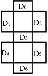
A more useful application of combinational encoder design is a binary to 7-segment encoder. The seven segments are given according
D
0D
1D
3D
4D
6Our truth table is:
D
2 [image:14.612.94.176.503.632.2]9.5. ENCODER 287
I
3I
2I
1I
0D
6D
5D
4D
3D
2D
1D
00
0
0
0
0
0
0
01
0
1
0
1
1
1
01
1
0
1
1
01
0
1
1
1
1
1
1
0
1
0
1
1
0
1
1
01
01
01
01
1
1
1
1
1
1
01
01
01
01
1
1
1
1
01
01
01
01
0
1
1
0
01
01
01
01
01
1
1
0
0
01
1
01
01
0
1
1
1
1
01
01
01
01
Deciding what to do with the remaining six entries of the truth table is easier with this circuit. This circuit should not be expected to encode an undefined combination of inputs, so we can leave them as ”don’t care” when we design the circuit. The boolean equations are
D
0= I
3+ I
1+ I
3I
2I
1I
0+ I
3I
2I
1I
0D
1= I
3+ I
2I
1+ I
2I
1+ I
2I
0D
2= I
2+ I
3I
2I
1I
0+ I
3I
2I
1I
0D
3= I
3+ I
1I
0+ I
2I
1D
4= I
1I
0+ I
2I
1I
0D
5= I
3+ I
2+ I
0D
6= I
3+ I
1I
0+ I
3I
2I
1+ I
3I
2I
1I
0+ I
3I
2I
1I
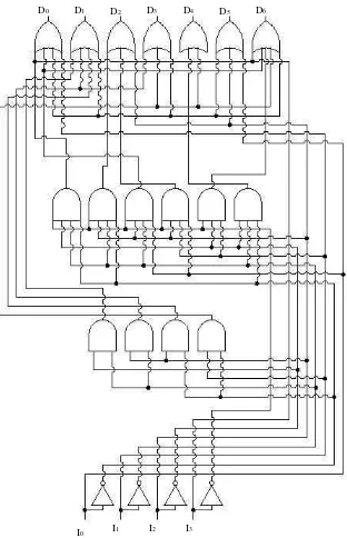
0and the circuit is
288 CHAPTER 9. COMBINATIONAL LOGIC FUNCTIONS
D0 D1 D2 D3 D4
[image:16.612.134.446.134.618.2]I1
Figure 9.1: Seven-segment decoder gate level diagram.
I0 I2 I3
9.6. DEMULTIPLEXERS
L1
I3
I1
I3
I3
I3
I2
I2
I2
I2
I3
I3
I3
I1
I2
I1
I2
I3
I2
I0
I3
I1
I3
I3
I3
I0
I2
I2
I2
I1
I1
I1
I0
I0
D6
I0
I1
I0
I1 I0
D5
D4
I2
I2
I1
I1
I0
I0
D3
I1
I1
I0
D2
I2
I2
I1
I1
I0
I0
D1
D0
L2
289
9.6
Demultiplexers
290 CHAPTER 9. COMBINATIONAL LOGIC FUNCTIONS
description sounds similar to the description given for a decoder, but a decoder is used to select among many devices while a demultiplexer is used to send a signal among many devices.
A demultiplexer is used often enough that it has its own schematic symbol
I
A
The truth table for a 1-to-2 demultiplexer is
D
0D
1I
0
0
1
1
A
0
1
0
1
D
00
0
1
0
D
10
0
0
1
Using our 1-to-2 decoder as part of the circuit, we can express this circuit easily
I
D
0
D
11-to-2 line
decoder
9.6. DEMULTIPLEXERS 291
L
1I
A
A
D
0D
1L
2This circuit can be expanded two different ways. You can increase the number of signals that get transmitted, or you can increase the number of inputs that get passed through. To increase the number of inputs that get passed through just requires a larger line decoder. Increasing the number of signals that get transmitted is even easier.
As an example, a device that passes one set of two signals among four signals is a ”two-bit 1-to-2 demultiplexer”. Its circuit is
I
0D
0I
1D
2D
1D
31-to-2
decoder
A
or by expressing the circuit as292 CHAPTER 9. COMBINATIONAL LOGIC FUNCTIONS
I
0D
0D
1D
2D
3A
I
1L
1I
0A
A
I
1A
A
D
0D
1D
2D
3L
2shows that it could be two one-bit 1-to-2 demultiplexers without changing its expected be-havior.
9.7. MULTIPLEXERS 293
9.7
Multiplexers
A multiplexer, abbreviated mux, is a device that has multiple inputs and one output.
The schematic symbol for multiplexers is
I
0I
1A
The truth table for a 2-to-1 multiplexer isD
I
1I
0A D
0
0
0
0
1
1
1
1
0
0
1
1
0
0
1
1
0
1
0
1
0
1
0
1
0
0
0
1
1
0
1
1
Using a 1-to-2 decoder as part of the circuit, we can express this circuit easily.
I
0I
1D
1-to-2 line
decoder
294 CHAPTER 9. COMBINATIONAL LOGIC FUNCTIONS
L
1A
A
I
0I
1D
L
2Multiplexers can also be expanded with the same naming conventions as demultiplexers. A 4-to-1 multiplexer circuit is
That is the formal definition of a multiplexer. Informally, there is a lot of confusion. Both demultiplexers and multiplexers have similar names, abbreviations, schematic symbols and circuits, so confusion is easy. The term multiplexer, and the abbreviation mux, are often used to also mean a demultiplexer, or a multiplexer and a demultiplexer working together. So when you hear about a multiplexer, it may mean something quite different.
9.8
Using multiple combinational circuits
As an example of using several circuits together, we are going to make a device that will have 16 inputs, representing a four digit number, to a four digit 7-segment display but using just one binary-to-7-segment encoder.
9.8. USING MULTIPLE COMBINATIONAL CIRCUITS 295
7-segment
encoder
Follow this circuit through and you can confirm that it matches the description given above. There are 16 primary inputs. There are two more inputs used to select which digit will be displayed. There are 28 outputs to control the four digit 7-segment display. Only four of the primary inputs are encoded at a time. You may have noticed a potential question though.
When one of the digits are selected, what do the other three digits display? Review the circuit for the demultiplexers and notice that any line not selected by the A input is zero. So the other three digits are blank. We don’t have a problem, only one digit displays at a time.
296 L1 A1 A1 A1 A1 A1 A1 A1 A1 A1 A1 A1 A1 A1 A1 A1 A1 I3 I1 I3 I3 I3 I2 I2 I2 I2 I3 I3 I3 I1 I2 I1 I2 I3 I2 I0 x I0 I1 I0
I1 I0
D5 D4 I2 I2 I1 I1 I0 I0 D3 I1 I1 I0 D2 I2 I2 I1 I1 I0 I0 D1 A0 A0 A0 A0 A0 A0 A0 A0 A0 A0 A0 A0 A0 A0 A0 A0 D0,0 D1,0 D2,0 D3,0 D0,1 D1,1 D2,1 D3,1 D0,2 D1,2 D2,2 D3,2 D0,3 D1,3 D2,3 D3,3 I0
CHAPTER 9. COMBINATIONAL LOGIC FUNCTIONS
L2 x I0 I0 I0 I1 I1 I1 I1 I2 I2 I2 I2 I3 I3 I3 I3 D0 I3 I1 I3 I3 I3 A1 A1 A1 A1 A1 A1 A1 A1 A1 A1 A1 A1 A1 A1 A1 A1 A1 A1 A1 A1 A1 A1 A1 A1 A1 A1 A1 A1 I0 I2 I2 I2 A0 A0 A0 A0 A0 A0 A0 A0 A0 A0 A0 A0 A0 A0 A0 A0 A0 A0 A0 A0 A0 A0 A0 A0 A0 A0 A0 A0 I1 I1 I1 D0 D0 D0 D0 D1 D1 D1 D1 D2 D2 D2 D2 D3 D3 D3 D3 D4 D4 D4 D4 D5 D5 D5 D5 D6 D6 D6 D6 I0 I0 Q0,0 Q0,1 Q0,2 Q0,3 Q1,0 Q1,1 Q1,2 Q1,3 Q2,0 Q2,1 Q2,2 Q2,3 Q3,0 Q3,1 Q3,2 Q3,3 Q4,0 Q4,1 Q4,2 Q4,3 Q5,0 Q5,1 Q5,2 Q5,3 Q6,0 Q6,1 Q6,2 Q6,3 D6 xx xx
Notice how quickly this large circuit was developed from smaller parts. This is true of most complex circuits: they are composed of smaller parts allowing a designer to abstract away some complexity and understand the circuit as a whole. Sometimes a designer can even take components that others have designed and remove the detail design work.
9.8. USING MULTIPLE COMBINATIONAL CIRCUITS 297
COUNTERS
Contents
11.1 Binary count sequence . . . 323
11.2 Asynchronous counters . . . 325
11.3 Synchronous counters . . . 332
11.4 Counter modulus . . . 338
*** INCOMPLETE ***
11.1
Binary count sequence
If we examine a four-bit binary count sequence from 0000 to 1111, a definite pattern will be evident in the ”oscillations” of the bits between 0 and 1:
324 CHAPTER 11. COUNTERS
0000
0001
0010
0011
0100
0101
0110
0111
1000
1001
1010
1011
1100
1101
1110
1111
Note how the least significant bit (LSB) toggles between 0 and 1 for every step in the count sequence, while each succeeding bit toggles at one-half the frequency of the one before it. The most significant bit (MSB) only toggles once during the entire sixteen-step count sequence: at the transition between 7 (0111) and 8 (1000).
If we wanted to design a digital circuit to ”count” in four-bit binary, all we would have to do is design a series of frequency divider circuits, each circuit dividing the frequency of a square-wave pulse by a factor of 2:
(LSB)
0
0
0
1
0
0
0
0
1
0
0
1
1
0
0
0
0
1
0
1
0
1
0
0
1
1
0
1
1
1
0
0
0
0
1
1
0
0
1
0
1
0
1
1
1
0
1
0
0
1
1
1
0
1
1
0
1
1
1
1
1
1
1
(MSB)
0
11.2. ASYNCHRONOUS COUNTERS 325
Vdd
signal
B
signal
A
J
C
K
Q
Q
A
B
0
0
1
1
0
1
1
0
0
0
1
1
0
1
1
0
0
0
1
1
0
1
1
0
If we consider the two signals (A and B) in this circuit to represent two bits of a binary number, signal A being the LSB and signal B being the MSB, we see that the count sequence is backward: from 11 to 10 to 01 to 00 and back again to 11. Although it might not be counting in the direction we might have assumed, at least it counts!
The following sections explore different types of counter circuits, all made with J-K flip-flops, and all based on the exploitation of that flip-flop’s toggle mode of operation.
• REVIEW:
• Binary count sequences follow a pattern of octave frequency division: the frequency of oscillation for each bit, from LSB to MSB, follows a divide-by-two pattern. In other words, the LSB will oscillate at the highest frequency, followed by the next bit at one-half the LSB’s frequency, and the next bit at one-half the frequency of the bit before it, etc.
• Circuits may be built that ”count” in a binary sequence, using J-K flip-flops set up in the ”toggle” mode.
11.2
Asynchronous counters
326 CHAPTER 11. COUNTERS
proper binary sequence. Examine the following binary count sequence, paying attention to patterns preceding the ”toggling” of a bit between 0 and 1:
0000
0001
0010
0011
0100
0101
0110
0111
1000
1001
1010
1011
1100
1101
1110
1111
Note that each bit in this four-bit sequence toggles when the bit before it (the bit having a lesser significance, or place-weight), toggles in a particular direction: from 1 to 0. Small arrows indicate those points in the sequence where a bit toggles, the head of the arrow pointing to the previous bit transitioning from a ”high” (1) state to a ”low” (0) state:
0000
0001
0010
0011
0100
0101
0110
0111
1000
1001
1010
1011
1100
1101
1110
1111
11.2. ASYNCHRONOUS COUNTERS
as the respective binary bits of the final, four-bit count:
Q0 Vdd Vdd 327 Q1 Vdd Q2 Vdd Q3 J C K Q ? Q J C K Q ? Q J C K Q ? Q J C K Q Q
If we used flip-flops with negative-edge triggering (bubble symbols on the clock inputs), we could simply connect the clock input of each flip-flop to the Q output of the flip-flop before it, so that when the bit before it changes from a 1 to a 0, the ”falling edge” of that signal would ”clock” the next flip-flop to toggle the next bit:
A four-bit "up" counter
Q0 Vdd Vdd Q1 Vdd Q2 Vdd Q3 J C K Q J C Q J C Q J C Q
Q K Q K Q K Q
This circuit would yield the following output waveforms, when ”clocked” by a repetitive source of pulses from an oscillator:
Clock
Q
00
Q
10
Q
20
Q
30
1
0
0
0
0
1
0
0
1
1
0
0
0
0
1
0
1
0
1
0
0
1
1
0
1
1
1
0
0
0
0
1
1
0
0
1
0
1
0
1
1
1
0
1
0
0
1
1
1
0
1
1
0
1
1
1
1
1
1
1
328 CHAPTER 11. COUNTERS
demonstrating how the clock signal need not be symmetrical to obtain reliable, ”clean” output bits in our four-bit binary sequence. In the very first flip-flop circuit shown in this chapter, I used the clock signal itself as one of the output bits. This is a bad practice in counter design, though, because it necessitates the use of a square wave signal with a 50% duty cycle (”high” time = ”low” time) in order to obtain a count sequence where each and every step pauses for the same amount of time. Using one J-K flip-flop for each output bit, however, relieves us of the necessity of having a symmetrical clock signal, allowing the use of practically any variety of high/low waveform to increment the count sequence.
As indicated by all the other arrows in the pulse diagram, each succeeding output bit is toggled by the action of the preceding bit transitioning from ”high” (1) to ”low” (0). This is the pattern necessary to generate an ”up” count sequence.
A less obvious solution for generating an ”up” sequence using positive-edge triggered flip-flops is to ”clock” each flip-flop using the Q’ output of the preceding flip-flop rather than the Q output. Since the Q’ output will always be the exact opposite state of the Q output on a J-K flip-flop (no invalid states with this type of flip-flop), a high-to-low transition on the Q output will be accompanied by a low-to-high transition on the Q’ output. In other words, each time the Q output of a flip-flop transitions from 1 to 0, the Q’ output of the same flip-flop will transition from 0 to 1, providing the positive-going clock pulse we would need to toggle a positive-edge triggered flip-flop at the right moment:
A different way of making a four-bit "up" counter
Q0
Vdd Vdd
Q1
Vdd
Q2
Vdd
Q3
J
C
K
Q J
C
Q J
C
Q J
C
Q
Q K Q K Q K Q
11.2. ASYNCHRONOUS COUNTERS
A simultaneous "up" and "down" counter
Q0 Vdd Vdd 329 Q1 Vdd Q2 Vdd Q3 J C K Q J C Q J C Q J C Q
Q K Q K Q K Q
Q0 Q1 Q2 Q3
"Up" count sequence
Q
00
Q
10
Q
20
Q
30
1
0
0
0
0
1
0
0
1
1
0
0
0
0
1
0
1
0
1
0
0
1
1
0
1
1
1
0
0
0
0
1
1
0
0
1
0
1
0
1
1
1
0
1
0
0
1
1
1
0
1
1
0
1
1
1
1
1
1
1
"Down" count sequence
Q
01
Q
11
Q
21
Q
31
0
1
1
1
1
0
1
1
0
0
1
1
1
1
0
1
0
1
0
1
1
0
0
1
0
0
0
1
1
1
1
0
0
1
1
0
1
0
1
0
0
0
1
0
1
1
0
0
0
1
0
0
1
0
0
0
0
0
0
0
330
the same time:
CHAPTER 11. COUNTERS
Pulse diagram showing (exaggerated) propagation delays
Q
00 1
Q
1Q
2Q
300
00
00
0
1
0
0
1
1
0
0
0
0
1
0
1
0
1
0
0
1
1
0
1
1
1
0
0
0
0
1
1
0
0
1
0
1
0
1
1
1
0
1
0
0
1
1
1
0
1
1
0
1
1
1
1
1
1
1
Accumulated
delay
As you can see, the more bits that toggle with a given clock pulse, the more severe the accumulated delay time from LSB to MSB. When a clock pulse occurs at such a transition point (say, on the transition from 0111 to 1000), the output bits will ”ripple” in sequence from LSB to MSB, as each succeeding bit toggles and commands the next bit to toggle as well, with a small amount of propagation delay between each bit toggle. If we take a close-up look at this effect during the transition from 0111 to 1000, we can see that there will be false output counts generated in the brief time period that the ”ripple” effect takes place:
Count
7
False
Count
counts
8
Q
01
0
0
0
0
delay
Q
11
1
0
0
0
delay
Q
21
1
1
0
0
delay
Q
30
0
0
0
1
11.2. ASYNCHRONOUS COUNTERS 331
then to 8. This behavior earns the counter circuit the name of ripple counter, or asynchronous counter.
In many applications, this effect is tolerable, since the ripple happens very, very quickly (the width of the delays has been exaggerated here as an aid to understanding the effects). If all we wanted to do was drive a set of light-emitting diodes (LEDs) with the counter’s outputs, for example, this brief ripple would be of no consequence at all. However, if we wished to use this counter to drive the ”select” inputs of a multiplexer, index a memory pointer in a microprocessor (computer) circuit, or perform some other task where false outputs could cause spurious errors, it would not be acceptable. There is a way to use this type of counter circuit in applications sensitive to false, ripple-generated outputs, and it involves a principle known as strobing.
Most decoder and multiplexer circuits are equipped with at least one input called the ”en-able.” The output(s) of such a circuit will be active only when the enable input is made active. We can use this enable input to strobe the circuit receiving the ripple counter’s output so that it is disabled (and thus not responding to the counter output) during the brief period of time in which the counter outputs might be rippling, and enabled only when sufficient time has passed since the last clock pulse that all rippling will have ceased. In most cases, the strobing signal can be the same clock pulse that drives the counter circuit:
Receiving circuit
EN
Outputs
Clock signal
Binary count input
Q0
Vdd Vdd
Q1
Vdd
Q2
Vdd
Q3
J
C
K
Q J
C
Q J
C
Q J
C Q
Q K Q K Q K Q
Counter circuit
332 CHAPTER 11. COUNTERS
Another disadvantage of the asynchronous, or ripple, counter circuit is limited speed. While all gate circuits are limited in terms of maximum signal frequency, the design of asynchronous counter circuits compounds this problem by making propagation delays additive. Thus, even if strobing is used in the receiving circuit, an asynchronous counter circuit cannot be clocked at any frequency higher than that which allows the greatest possible accumulated propagation delay to elapse well before the next pulse.
The solution to this problem is a counter circuit that avoids ripple altogether. Such a counter circuit would eliminate the need to design a ”strobing” feature into whatever digi-tal circuits use the counter output as an input, and would also enjoy a much greater operating speed than its asynchronous equivalent. This design of counter circuit is the subject of the next section.
• REVIEW:
• An ”up” counter may be made by connecting the clock inputs of positive-edge triggered J-K flip-flops to the Q’ outputs of the preceding flip-flops. Another way is to use edge triggered flip-flops, connecting the clock inputs to the Q outputs of the preceding flip-flops. In either case, the J and K inputs of all flip-flops are connected to V cc or Vdd so
as to always be ”high.”
• Counter circuits made from cascaded J-K flip-flops where each clock input receives its pulses from the output of the previous flip-flop invariably exhibit a ripple effect, where false output counts are generated between some steps of the count sequence. These types of counter circuits are called asynchronous counters, or ripple counters.
• Strobing is a technique applied to circuits receiving the output of an asynchronous (ripple) counter, so that the false counts generated during the ripple time will have no ill effect. Essentially, the enable input of such a circuit is connected to the counter’s clock pulse in such a way that it is enabled only when the counter outputs are not changing, and will be disabled during those periods of changing counter outputs where ripple occurs.
11.3
Synchronous counters
11.3. SYNCHRONOUS COUNTERS
Q0 Q1 Q2 Q3
333
? J
C
Q ?
J
C
Q ?
J
C
Q ?
J
C
Q
?
K Q
?
K Q
?
K Q
?
K Q
Now, the question is, what do we do with the J and K inputs? We know that we still have to maintain the same divide-by-two frequency pattern in order to count in a binary sequence, and that this pattern is best achieved utilizing the ”toggle” mode of the flip-flop, so the fact that the J and K inputs must both be (at times) ”high” is clear. However, if we simply connect all the J and K inputs to the positive rail of the power supply as we did in the asynchronous circuit, this would clearly not work because all the flip-flops would toggle at the same time: with each and every clock pulse!
This circuit will not function as a counter!
Q0
Vdd Vdd
Q1
Vdd
Q2
Vdd
Q3
J
C
K
Q J
C
Q J
C
Q J
C
Q
Q K Q K Q K Q
Let’s examine the four-bit binary counting sequence again, and see if there are any other patterns that predict the toggling of a bit. Asynchronous counter circuit design is based on the fact that each bit toggle happens at the same time that the preceding bit toggles from a ”high” to a ”low” (from 1 to 0). Since we cannot clock the toggling of a bit based on the toggling of a previous bit in a synchronous counter circuit (to do so would create a ripple effect) we must find some other pattern in the counting sequence that can be used to trigger a bit toggle:
334 CHAPTER 11. COUNTERS
0000
0001
0010
0011
0100
0101
0110
0111
1000
1001
1010
1011
1100
1101
1110
1111
This pattern is also something we can exploit in designing a counter circuit. If we enable each J-K flip-flop to toggle based on whether or not all preceding flip-flop outputs (Q) are ”high,” we can obtain the same counting sequence as the asynchronous circuit without the ripple effect, since each flip-flop in this circuit will be clocked at exactly the same time:
A four-bit synchronous "up" counter
Q0
Vdd
Q1 Q2 Q3
J
C
K
Q J
C
Q J
C
Q J
C
Q
Q K Q K Q K Q
This flip-flop toggles on every clock pulse
This flip-flop toggles only if Q0 is "high"
This flip-flop toggles only if Q0 AND Q1 are "high"
This flip-flop toggles only if Q0 AND Q1 AND Q2 are "high"
The result is a four-bit synchronous ”up” counter. Each of the higher-order flip-flops are made ready to toggle (both J and K inputs ”high”) if the Q outputs of all previous flip-flops are ”high.” Otherwise, the J and K inputs for that flip-flop will both be ”low,” placing it into the ”latch” mode where it will maintain its present output state at the next clock pulse. Since the first (LSB) flip-flop needs to toggle at every clock pulse, its J and K inputs are connected to V cc
or Vdd , where they will be ”high” all the time. The next flip-flop need only ”recognize” that the
11.3. SYNCHRONOUS COUNTERS 335
the remaining flip-flops should be made ready to toggle only when all lower-order output bits are ”high,” thus the need for AND gates.
To make a synchronous ”down” counter, we need to build the circuit to recognize the appro-priate bit patterns predicting each toggle state while counting down. Not surprisingly, when we examine the four-bit binary count sequence, we see that all preceding bits are ”low” prior to a toggle (following the sequence from bottom to top):
0000
0001
0010
0011
0100
0101
0110
0111
1000
1001
1010
1011
1100
1101
1110
1111
336
A four-bit synchronous "down" counter
Q0
Vdd
CHAPTER 11. COUNTERS
Q1 Q2 Q3
J
C
K
Q J
C
Q J
C
Q J
C
Q
Q K Q K Q K Q
This flip-flop toggles on every clock pulse
This flip-flop toggles only if Q0 is "high"
This flip-flop toggles only if Q0 AND Q1 are "high"
This flip-flop toggles only if Q0 AND Q1 AND Q2 are "high"
Taking this idea one step further, we can build a counter circuit with selectable between ”up” and ”down” count modes by having dual lines of AND gates detecting the appropriate bit conditions for an ”up” and a ”down” counting sequence, respectively, then use OR gates to combine the AND gate outputs to the J and K inputs of each succeeding flip-flop:
A four-bit synchronous "up/down" counter
Vdd Q0 Q1 Q2 Q3
Up/Down
J
C
K Q
Q J
C
K Q
Q J
C
K Q
Q J
C
K Q
Q
This circuit isn’t as complex as it might first appear. The Up/Down control input line simply enables either the upper string or lower string of AND gates to pass the Q/Q’ outputs to the succeeding stages of flip-flops. If the Up/Down control line is ”high,” the top AND gates become enabled, and the circuit functions exactly the same as the first (”up”) synchronous counter circuit shown in this section. If the Up/Down control line is made ”low,” the bottom AND gates become enabled, and the circuit functions identically to the second (”down” counter) circuit shown in this section.
11.3. SYNCHRONOUS COUNTERS
Counter in "up" counting mode
Vdd Vdd
337
Q0 Q1 Q2 Q3
Up/ Down
J
C
K
Q J
C
Q J
C
Q J
C Q
Q K Q K Q K Q
Here, shown in the ”down” counting mode, with the same grey coloring representing dis-abled circuitry:
Counter in "down" counting mode
Vdd Vdd Q0 Q1 Q2 Q3
Up/ Down
J
C
K
Q J
C
Q J
C
Q J
C Q
Q K Q K Q K Q
Up/down counter circuits are very useful devices. A common application is in machine motion control, where devices called rotary shaft encoders convert mechanical rotation into a series of electrical pulses, these pulses ”clocking” a counter circuit to track total motion:
Light sensor
(phototransistor)
LED
Q
0Q
1Q
2Q
3Counter
Rotary shaft encoder
338 CHAPTER 11. COUNTERS
encoder/decoding circuit having the ability to discriminate between different directions. If we re-design the encoder to have two sets of LED/phototransistor pairs, those pairs aligned such that their square-wave output signals are 90o out of phase with each other, we
have what is known as a quadrature output encoder (the word ”quadrature” simply refers to a 90o angular separation). A phase detection circuit may be made from a D-type flip-flop, to
distinguish a clockwise pulse sequence from a counter-clockwise pulse sequence:
Light sensor (phototransistor)
LED D
C
Q
Rotary shaft encoder (quadrature output)
Q
Q0 Q1 Q2 Q3
Up/Down
Counter
When the encoder rotates clockwise, the ”D” input signal square-wave will lead the ”C” input square-wave, meaning that the ”D” input will already be ”high” when the ”C” transitions from ”low” to ”high,” thus setting the D-type flip-flop (making the Q output ”high”) with every clock pulse. A ”high” Q output places the counter into the ”Up” count mode, and any clock pulses received by the clock from the encoder (from either LED) will increment it. Conversely, when the encoder reverses rotation, the ”D” input will lag behind the ”C” input waveform, meaning that it will be ”low” when the ”C” waveform transitions from ”low” to ”high,” forcing the D-type flip-flop into the reset state (making the Q output ”low”) with every clock pulse. This ”low” signal commands the counter circuit to decrement with every clock pulse from the encoder.
SHIFT REGISTERS
Contents
12.1 Introduction . . . .
12.2 Serial-in/serial-out shift register . . . . 12.2.1 Serial-in/serial-out devices . . . .
12.3 Parallel-in, serial-out shift register . . . . 12.3.1 Parallel-in/serial-out devices . . . . 12.3.2 Practical applications . . . .
12.4 Serial-in, parallel-out shift register . . . . 12.4.1 Serial-in/ parallel-out devices . . . . 12.4.2 Practical applications . . . .
12.5 Parallel-in, parallel-out, universal shift register 12.5.1 Parallel-in/ parallel-out and universal devices . 12.5.2 Practical applications . . . .
12.6 Ring counters . . . . 12.6.1 Johnson counters . . . .
12.7 references . . . .
. . . . . . . . . . . . . . . . . . . . . . . . . . . . . . . . . . . . . . . . . . . . . . . . . . . . . . . . . . . . . . . . . . . . . . . . . . . . . . . . . . . . . . . . . . . . . . . . . . . . . . . . . . . . . . . . . . . . . . . . . . . . . . . . . . . . . . . . . . . . . . . . . . . . . . . . . . . . . . . . . . . . . . . . . . . . . . . . . . . . . . . . . . . . . . . . . . . . . . . . . . . . . . . . . . . . . . . . . . . . . . . . . 339 342 346 351 354 360 362 363 369 371 376 380 382 385 395
Original author: Dennis Crunkilton
12.1
Introduction
Shift registers, like counters, are a form of sequential logic. Sequential logic, unlike combina-tional logic is not only affected by the present inputs, but also, by the prior history. In other words, sequential logic remembers past events.
Shift registers produce a discrete delay of a digital signal or waveform. A waveform syn-chronized to a clock, a repeating square wave, is delayed by ”n” discrete clock times, where ”n” is the number of shift register stages. Thus, a four stage shift register delays ”data in”
340 CHAPTER 12. SHIFT REGISTERS
by four clocks to ”data out”. The stages in a shift register are delay stages, typically type ”D” Flip-Flops or type ”JK” Flip-flops.
Formerly, very long (several hundred stages) shift registers served as digital memory. This obsolete application is reminiscent of the acoustic mercury delay lines used as early computer memory.
Serial data transmission, over a distance of meters to kilometers, uses shift registers to convert parallel data to serial form. Serial data communications replaces many slow parallel data wires with a single serial high speed circuit.
Serial data over shorter distances of tens of centimeters, uses shift registers to get data into and out of microprocessors. Numerous peripherals, including analog to digital converters, digital to analog converters, display drivers, and memory, use shift registers to reduce the amount of wiring in circuit boards.
Some specialized counter circuits actually use shift registers to generate repeating wave-forms. Longer shift registers, with the help of feedback generate patterns so long that they look like random noise, pseudo-noise.
Basic shift registers are classified by structure according to the following types:
• Serial-in/serial-out
• Parallel-in/serial-out
• Serial-in/parallel-out
• Universal parallel-in/parallel-out
• Ring counter
data in
clock
stage A stage B stage C stage D
data out
Serial-in, serial-out shift register with 4-stages
Above we show a block diagram of a serial-in/serial-out shift register, which is 4-stages long. Data at the input will be delayed by four clock periods from the input to the output of the shift register.
12.1. INTRODUCTION
DA DB DC DD
341
data in
clock
stage A stage B stage C stage D
data out
Parallel-in, serial-out shift register with 4-stages
Data is loaded into all stages at once of a parallel-in/serial-out shift register. The data is then shifted out via ”data out” by clock pulses. Since a 4- stage shift register is shown above, four clock pulses are required to shift out all of the data. In the diagram above, stage D data will be present at the ”data out” up until the first clock pulse; stage C data will be present at ”data out” between the first clock and the second clock pulse; stage B data will be present between the second clock and the third clock; and stage A data will be present between the third and the fourth clock. After the fourth clock pulse and thereafter, successive bits of ”data in” should appear at ”data out” of the shift register after a delay of four clock pulses.
If four switches were connected to DA through DD , the status could be read into a
micro-processor using only one data pin and a clock pin. Since adding more switches would require no additional pins, this approach looks attractive for many inputs.
data in
clock
stage A
QA
stage B
QB
stage C
QC
stage D
QD
data out
Serial-in, parallel-out shift register with 4-stages
Above, four data bits will be shifted in from ”data in” by four clock pulses and be available at QA through QD for driving external circuitry such as LEDs, lamps, relay drivers, and horns.
After the first clock, the data at ”data in” appears at QA . After the second clock, The old
QA data appears at QB ; QA receives next data from ”data in”. After the third clock, QB data is
342
DA DB DC
CHAPTER 12. SHIFT REGISTERS
DD
data in
clock mode
data out
stage A
QA
stage B
QB
stage C
QC
stage D
QD
Parallel-in, parallel-out shift register with 4-stages
A parallel-in/laralel-out shift register combines the function of the parallel-in, serial-out shift register with the function of the serial-in, parallel-out shift register to yields the univer-sal shift register. The ”do anything” shifter comes at a price– the increased number of I/O (Input/Output) pins may reduce the number of stages which can be packaged.
Data presented at DA through DD is parallel loaded into the registers. This data at QA
through QD may be shifted by the number of pulses presented at the clock input. The shifted data is available at QA through QD . The ”mode” input, which may be more than one input,
controls parallel loading of data from DA through DD , shifting of data, and the direction of
shifting. There are shift registers which will shift data either left or right.
data out data in
clock
stage A stage B stage C stage D
QD
Ring Counter, shift register output fed back to input
If the serial output of a shift register is connected to the serial input, data can be perpetually shifted around the ring as long as clock pulses are present. If the output is inverted before being fed back as shown above, we do not have to worry about loading the initial data into the ”ring counter”.
12.2
Serial-in/serial-out shift register
Serial-in, serial-out shift registers delay data by one clock time for each stage. They will store a bit of data for each register. A serial-in, serial-out shift register may be one to 64 bits in length, longer if registers or packages are cascaded.
12.2. SERIAL-IN/SERIAL-OUT SHIFT REGISTER 343
clock changes for low to high. We may want to synchronize the data to a system wide clock in a circuit board to improve the reliability of a digital logic circuit.
data in
clock D
C
Q
clock
data in Q
QA
t1 t2 t3 t4
Data present at clock time is transfered from D to Q.
The obvious point (as compared to the figure below) illustrated above is that whatever ”data in” is present at the D pin of a type D FF is transfered from D to output Q at clock time. Since our example shift register uses positive edge sensitive storage elements, the output Q follows the D input when the clock transitions from low to high as shown by the up arrows on the diagram above. There is no doubt what logic level is present at clock time because the data is stable well before and after the clock edge. This is seldom the case in multi-stage shift registers. But, this was an easy example to start with. We are only concerned with the positive, low to high, clock edge. The falling edge can be ignored. It is very easy to see Q follow D at clock time above. Compare this to the diagram below where the ”data in” appears to change with the positive clock edge.
data in
clock D
C
Q
clock
data in Q
QC ?
QW ?
t1 t2 t3
? ?
Does the clock t1 see a 0 or a 1 at data in at D? Which output is correct,
QC or QW ?
Since ”data in” appears to changes at clock time t1 above, what does the type D FF see at
clock time? The short over simplified answer is that it sees the data that was present at D prior to the clock. That is what is transfered to Q at clock time t1 . The correct waveform is QC .
At t1 Q goes to a zero if it is not already zero. The D register does not see a one until time t 2 ,
344
t1
clock
clock C data in
Q
QA
CHAPTER 12. SHIFT REGISTERS
t2 t3 t4
data in D Q
delay of 1 clock period
Data present tH before clock time at D is transfered to Q.
Since data, above, present at D is clocked to Q at clock time, and Q cannot change until the next clock time, the D FF delays data by one clock period, provided that the data is already synchronized to the clock. The QA waveform is the same as ”data in” with a one clock period
delay.
A more detailed look at what the input of the type D Flip-Flop sees at clock time follows. Refer to the figure below. Since ”data in” appears to changes at clock time (above), we need further information to determine what the D FF sees. If the ”data in” is from another shift register stage, another same type D FF, we can draw some conclusions based on data sheet information. Manufacturers of digital logic make available information about their parts in data sheets, formerly only available in a collection called a data book. Data books are still available; though, the manufacturer’s web site is the modern source.
clock
data in D
t
SQ
t
Ht
PData must be present (tS) before the clock and after(tH) the clock. Data is
delayed from D to Q by propagation delay (tP)
The following data was extracted from the CD4006b data sheet for operation at 5V DC , which serves as an example to illustrate timing.
(http://focus.ti.com/docs/prod/folders/print/cd4006b.html)
• tS =100ns
• tH =60ns
12.2. SERIAL-IN/SERIAL-OUT SHIFT REGISTER 345
tS is the setup time, the time data must be present before clock time. In this case data must be present at D 100ns prior to the clock. Furthermore, the data must be held for hold time tH =60ns after clock time. These two conditions must be met to reliably clock data from D to Q
of the Flip-Flop.
There is no problem meeting the setup time of 60ns as the data at D has been there for the whole previous clock period if it comes from another shift register stage. For example, at a clock frequency of 1 Mhz, the clock period is 1000 µs, plenty of time. Data will actually be present for 1000µs prior to the clock, which is much greater than the minimum required t S of
60ns.
The hold time tH =60ns is met because D connected to Q of another stage cannot change any faster than the propagation delay of the previous stage tP =200ns. Hold time is met as long as
the propagation delay of the previous D FF is greater than the hold time. Data at D driven by another stage Q will not change any faster than 200ns for the CD4006b.
To summarize, output Q follows input D at nearly clock time if Flip-Flops are cascaded into a multi-stage shift register.
QA
data in D
C
Q
Q D
C
Q
QB
Q D
C
QC
Q data out
Q
clock
Serial-in, serial-out shift register using type "D" storage elements
Three type D Flip-Flops are cascaded Q to D and the clocks paralleled to form a three stage shift register above.
QA
data in J
C
K Q
Q J
C
K
QB
Q J
C
Q K
QC Q data out
Q
clock
Serial-in, serial-out shift register using type "JK" storage elements
Type JK FFs cascaded Q to J, Q’ to K with clocks in parallel to yield an alternate form of the shift register above.
346 CHAPTER 12. SHIFT REGISTERS
The waveforms below are applicable to either one of the preceding two versions of the serial-in, serial-out shift register. The three pairs of arrows show that a three stage shift register temporarily stores 3-bits of data and delays it by three clock periods from input to output.
t
1clock
data in
Q
AQ
BQ
Ct
2t
3t
4At clock time t1 a ”data in” of 0 is clocked from D to Q of all three stages. In particular, D of stage A sees a logic 0, which is clocked to QA where it remains until time t2 .
At clock time t2 a ”data in” of 1 is clocked from D to QA . At stages B and C, a 0, fed from
preceding stages is clocked to QB and QC .
At clock time t3 a ”data in” of 0 is clocked from D to QA . QA goes low and stays low for
the remaining clocks due to ”data in” being 0. QB goes high at t3 due to a 1 from the previous
stage. QC is still low after t3 due to a low from the previous stage.
QC finally goes high at clock t4 due to the high fed to D from the previous stage QB . All
earlier stages have 0s shifted into them. And, after the next clock pulse at t 5 , all logic 1s will
have been shifted out, replaced by 0s
12.2.1
Serial-in/serial-out devices
We will take a closer look at the following parts available as integrated circuits, courtesy of Texas Instruments. For complete device data sheets follow the links.
• CD4006b 18-bit serial-in/ serial-out shift register
(http://focus.ti.com/docs/prod/folders/print/cd4006b.html)
• CD4031b 64-bit serial-in/ serial-out shift register
(http://focus.ti.com/docs/prod/folders/print/cd4031b.html)
• CD4517b dual 64-bit serial-in/ serial-out shift register
(http://focus.ti.com/docs/prod/folders/print/cd4517b.html)
The following serial-in/ serial-out shift registers are 4000 series CMOS (Complementary Metal Oxide Semiconductor) family parts. As such, They will accept a V DD , positive power
12.2. SERIAL-IN/SERIAL-OUT SHIFT REGISTER
3
clock
1
CL
CL
4
CL
CL
D2 D2 +4 D2 +5
CL
CL
CL and CL to all 18-stages & latch.
D1 +4 13
2 5
CL
8
D4 D4 +4 D4 +5 9
D3 D3 +4 10
VSS ( pin 7) = Gnd, VDD (pin 14) = +3 to +18 VDC
347
D1
latch
11 CL
12 6
CL
CL
CD4006b Serial-in/ serial-out shift register
The 18-bit CD4006b consists of two stages of 4-bits and two more stages of 5-bits with a an output tap at 4-bits. Thus, the 5-bit stages could be used as 4-bit shift registers. To get a full 18-bit shift register the output of one shift register must be cascaded to the input of another and so on until all stages create a single shift register as shown below.
+5V
VDD
14
D2+5
D1+4
13 12
D2+4
11 10
D3+4
D4+5
D4+4
9 8
Out
Q
D
1
Clock
Data
D1
2 3
cl
4
D2
Clock
D1+4 delayed
5
D3
6
D4
7 VSS
348 CHAPTER 12. SHIFT REGISTERS
A CD4031 64-bit serial-in/ serial-out shift register is shown below. A number of pins are not connected (nc). Both Q and Q’ are available from the 64th stage, actually Q 64 and Q’64 . There
is also a Q64 ”delayed” from a half stage which is delayed by half a clock cycle. A major feature
is a data selector which is at the data input to the shift register.
VDD
16
Data 1
15 nc
14 nc
13 nc
12 nc
11
mode control
CLD
10 9
delayed clock out
D
C
Q
64-stages
Q D Q
1
Data 2 2
clock 3 nc
4 nc
5 6 7
Q64
8
VSS
Q64
Q64 delayed
CD4031 64-bit serial-in/ serial-out shift register
12.2. SERIAL-IN/SERIAL-OUT SHIFT REGISTER
VDD
mode control = logic high
nc 15 14 nc 13 nc 12 nc 11 10 CLD 9 349 Data 1 VDD 16 mode control delayed clock out
D C Q 64-stages Q D Q
t
1t
2t
3t
4clock
clock
Q64
1 2
clock Data 2 3 nc 4 nc 5 Q64 6 7 Q64 8 VSS
64 clocks 64 clocks
CD4031 64-bit serial-in/ serial-out shift register recirculating data.
The ”data 2” above is wired to the Q64 output of the shift register. With ”mode control” high,
the Q64 output is routed back to the shifter data input D. Data will recirculate from output to
input. The data will repeat every 64 clock pulses as shown above. The question that arises is how did this data pattern get into the shift register in the first place?
VDD
mode control = logic low
VDD 16 data 1 nc 15 14 nc 13 nc 12 nc 11 10 CLD 9
t1 t2 t64 t65
D
C
mode control delayed clock out
Q 64-stages Q D Q clock data 1 Q64 123 Datanc clock2 4 nc 5 Q64 6 7 Q64 8 VSS
350 CHAPTER 12. SHIFT REGISTERS
With ”mode control” low, the CD4031 ”data 1” is selected for input to the shifter. The output, Q64 , is not recirculated because the lower data selector gate is disabled. By disabled we mean
that the logic low ”mode select” inverted twice to a low at the lower NAND gate prevents it for passing any signal on the lower pin (data 2) to the gate output. Thus, it is disabled.
VDD
3 to 18 VDC Q16B
15
Q48B
14
WE C D
WE D C
WEB
13
16
CL8
12
32
Q64B
11
48
Q32B
10
DB
9
64
16
16 32 48 64
1
Q16A
2
Q48A
3 4 5
Q64A
6
Q32A
7
DA
8
VSS GND
WEA CLA
CD4517b dual 64-bit serial-in/ serial-out shift register
A CD4517b dual 64-bit shift register is shown above. Note the taps at the 16th, 32nd, and 48th stages. That means that shift registers of those lengths can be configured from one of the 64-bit shifters. Of course, the 64-bit shifters may be cascaded to yield an 80-bit, 96-bit, 112-bit, or 128-bit shift register. The clock CLA and CLB need to be paralleled when cascading the two
shifters. WEB and WEB are grounded for normal shifting operations. The data inputs to the
shift registers A and B are DA and DB respectively.
12.3. PARALLEL-IN, SERIAL-OUT SHIFT REGISTER
data in
clock
5V
VDD
16
Q16B
15
WEB
Q48B
14
WE C D
WE D C
351
Q16B out
CL8 Q64B
12
32
Q32B
10
48 64
DB
9 13
16
11
16 32 48 64
1
Q16A
data in
clock
2
Q48A
3
WEA
4
CLA
5 6
Q64A Q32A
7
DA
8 VSS
Q64A out
CD4517b dual 64-bit serial-in/ serial-out shift register, wired for 16-shift register, 64-bit shift register
Above we show A CD4517b wired as a 16-bit shift register for section B. The clock for section B is CLB . The data is clocked in at CLB . And the data delayed by 16-clocks is picked of off
Q16B . WEB , the write enable, is grounded.
Above we also show the same CD4517b wired as a 64-bit shift register for the independent section A. The clock for section A is CLA . The data enters at CLA . The data delayed by 64-clock
pulses is picked up from Q64A . WEA , the write enable for section A, is grounded.
12.3
Parallel-in, serial-out shift register
352
DA DB DC
CHAPTER 12. SHIFT REGISTERS
DD
data in
clock
stage A stage B stage C stage D
data out
Parallel-in, serial-out shift register with 4-stages
Below we take a close look at the internal details of a 3-stage parallel-in/ serial-out shift register. A stage consists of a type D Flip-Flop for storage, and an AND-OR selector to de-termine whether data will load in parallel, or shift stored data to the right. In general, these elements will be replicated for the number of stages required. We show three stages due to space limitations. Four, eight or sixteen bits is normal for real parts.
DA
QA
D Q D
C
Q Q
DB
QB Q
DC
QC D
C
Q
Q SO
SI C
CLK
SHIFT/LD = 0
Parallel-in/ serial-out shift register showing parallel load path
Above we show the parallel load path when SHIFT/LD’ is logic low. The upper NAND gates serving DA DB DC are enabled, passing data to the D inputs of type D Flip-Flops QA QB DC
respectively. At the next positive going clock edge, the data will be clocked from D to Q of the three FFs. Three bits of data will load into QA QB DC at the same time.
The type of parallel load just described, where the data loads on a clock pulse is known as synchronous load because the loading of data is synchronized to the clock. This needs to be differentiated from asynchronous load where loading is controlled by the preset and clear pins of the Flip-Flops which does not require the clock. Only one of these load methods is used within an individual device, the synchronous load being more common in newer devices.
DA
DAA
SI
QA D
C
Q Q
DB
DBB D
C
Q DC QB
Q DCC
QC D
C
Q
Q SO
CLK
SHIFT/LD = 1
12.3. PARALLEL-IN, SERIAL-OUT SHIFT REGISTER 353
The shift path is shown above when SHIFT/LD’ is logic high. The lower AND gates of the pairs feeding the OR gate are enabled giving us a shift register connection of SI to D A , QA
to DB , QB to DC , QC to SO. Clock pulses will cause data to be right shifted out to SO on
successive pulses.
The waveforms below show both parallel loading of three bits of data and serial shifting of this data. Parallel data at DA DB DC is converted to serial data at SO.
t1
clock
SHIFT/LD
t2 t3 t4
data in
DA
DB
DC
QA
QB
QC (SO)
1
0
1
1
0
1
Parallel-in/ serial-out shift register load/shift waveforms
What we previously described with words for parallel loading and shifting is now set down as waveforms above. As an example we present 101 to the parallel inputs D AA DBB DCC . Next, the SHIFT/LD’ goes low enabling loading of data as opposed to shifting of data. It needs to be low a short time before and after the clock pulse due to setup and hold requirements. It is considerably wider than it has to be. Though, with synchronous logic it is convenient to make it wide. We could have made the active low SHIFT/LD’ almost two clocks wide, low almost a clock before t1 and back high just before t3 . The important factor is that it needs to be low
around clock time t1 to enable parallel loading of the data by the clock.
Note that at t1 the data 101 at DA DB DC is clocked from D to Q of the Flip-Flops as shown
354
t1