Pleasecitethisarticleinpressas:B.Mardiana,etal.,AnalysesforvariousdopingstructuresofSOI-basedopticalphasemodulatorusingfree carrierdispersioneffect,Optik-Int.J.LightElectronOpt.(2013),http://dx.doi.org/10.1016/j.ijleo.2013.09.050
ARTICLE IN PRESS
GModelIJLEO-53972; No.ofPages4
Optikxxx (2013) xxx–xxx
ContentslistsavailableatScienceDirect
Optik
j o ur na l h o m e p a g e :w w w . e l s e v i e r . d e / i j l e o
Analyses
for
various
doping
structures
of
SOI-based
optical
phase
modulator
using
free
carrier
dispersion
effect
B.
Mardiana
a,b,∗,
Sahbudin
Shaari
a,
P.
Susthitha
Menon
a,
H.
Hazura
a,b,
A.R.
Hanim
a,b,
N.
Arsad
a,
H.
Abdullah
aaInstituteofMicroengineeringandNanoelectronics,UniversitiKebangsaanMalaysia,43600UKMBangi,Malaysia
bFacultyofElectronicandComputerEngineering,UniversitiTeknikalMalaysiaMelaka(UTeM),HangTuahJaya,76100DurianTunggal,Melaka,Malaysia
a
r
t
i
c
l
e
i
n
f
o
Articlehistory: Received30April2013 Accepted16September2013
Available online xxx
a
b
s
t
r
a
c
t
Thispaperhighlightsthestudyonvariousstructureofsilicon-on-insulator(SOI)opticalphase
modula-torsbasedonfreecarrierdispersioneffect.TheproposedmodulatorsemploytheforwardbiasedP-I-N
diodestructureintegratedinthewaveguideandwillbeworkingat1.55mopticaltelecommunications
wavelength.Threekindsofstructurearecomparedsystematicallywherethep+andn+dopingpositions
arevaried.ThemodelingandcharacterizationoftheSOIphasemodulatorswascarriedoutby3D
numer-icalsimulationpackage.Ourresultsshowthatthepositionofdopingregionshaveagreatinfluencesto
thedeviceperformance.Itwasdiscoveredthatthebeststructureinthisworkdemonstratedmodulation
efficiencyof0.015Vcmwithalengthof155m.
© 2013 Published by Elsevier GmbH.
1. Introduction
Recently, silicon-on-insulator (SOI) based optical modulator have earned an evolving interest due to its significant role in theinter-chipsopticalinterconnect.Silicon-on-insulator(SOI) sub-strates are widely usedto fabricate optoelectronic devices due tothehighindexcontrastbetweenthesilicon coreandthe sil-icacladding[1].Furthermore,siliconhasproventobearelatively cheapermaterialcomparedtootherIII–Vsemiconductor materi-alsand suitableforintegratedphotonicsystem.Inaddition,SOI hassignificantadvantagesinwhichithasverylowbendingloss [2].Therefore,morecompactdevicecanbematerializedwiththe utilizationofSOIasthesubstratematerial[3].
Phasemodulatorareusedtochangethedatasignalfrom electri-caldomaintoopticaldomain.Themosteffectivewaytomodulate thesignalinsilicon-basedmodulatorisbyfreecarrierdispersion effect.Thismechanismisusedduetothefactsthatunstrainedpure crystalsilicondoesnothaveelectro-opticeffectsuchusPockels effect,KerreffectandFranz–Keldysheffect[4].Tocreatethefree carrierdispersioneffectinsiliconmodulator,theelectrical struc-turehasbeeneitheraP-I-Ndiodeininjectionmode,aPNdiode indepletionmodeorwiththeuseofMOScapacitor.Thecarrier injectionP-I-Ndiodestructureiswidelyimplementedaselectrical
∗Correspondingauthorat:InstituteofMicroengineeringandNanoelectronics,
UniversitiKebangsaanMalaysia,43600UKMBangi,Malaysia. E-mailaddress:[email protected](B.Mardiana).
structureofmodulatorduetoitshighefficiencyandsmallestsize [5].
Inthispaper,theP-I-NSOIphasemodulatorsaredesignedin threestructureswithdifferentkindofdopingpositions.The three-dimensional(3D)semiconductorsimulationpackageSILVACOwas usedforthis purpose.In thispaper,the3Ddesignsareutilized becauseofthedesignsconsiderthedopingpositionsvariationsin theinz-axis.Therefore,thedispersioneffectoffreecarrierelectrons andholescanbeexaminedalongz-axis.
2. Theory
Themodelingof theopticalmodulator wasperformedusing acommercialnumericalsimulator3D-SILVACOwhichemploya drift-diffusionapproach[6].ThePoisson,carriercontinuityand cur-rentdensityequationsaresolvednumericallyinthreedimensions subjecttothedevice’sgeometryandboundaryconditionsimposed bythedevice’scontactsandbiasingconditions.Thebasicequation tobesolvedateachnodeduringasimulationtoolisgivenbythe Poissonequation:
∇
(∈∇
)=−q[n−p+˙(N− A−N+ D+N
− AA−N
+
DD)] (1) where istheelectrostaticpotential,εisepsilon,qisthe elec-troniccharge,nandpisthedensityofmovablecarriers,NA−andND+ arerespectivelytheconcentrationofionizeddonorsandrecipients respectivelywhiletheNAA− andNDD+ istheconcentrationoftraps carrierthatservesastherecipientanddonorionized.
Themodulatorsoperationismodeledbytakingintoaccountthe carriergenerationinopticalandthermal,recombinationprocess 0030-4026/$–seefrontmatter© 2013 Published by Elsevier GmbH.
Pleasecitethisarticleinpressas:B.Mardiana,etal.,AnalysesforvariousdopingstructuresofSOI-basedopticalphasemodulatorusingfree carrierdispersioneffect,Optik-Int.J.LightElectronOpt.(2013),http://dx.doi.org/10.1016/j.ijleo.2013.09.050
ARTICLE IN PRESS
GModelIJLEO-53972; No.ofPages4
2 B.Mardianaetal./Optikxxx (2013) xxx–xxx
and theprocess of carrier driftand diffusion. Continuity equa-tionfortheelectronandholecarriers describestherelationship betweentheseprocessesandisgivenby;
∂n
∂t =Gn−Rn+ 1
q
∇
· Jn (2)∂p
∂t =Gp−Rp+ 1
q
∇
· Jp (3)whereGnandGpwhichistherateofproductionofelectronsand
holesresulting fromexternal effects suchasopticalexcitations inhigh-energyphotons,whileJnandJparetheelectronandhole
currentdensity.RnandRpisthecarrierrecombinationrate.
Generally,currentflowoccursinthecombinedprocessof diffu-sionanddriftinthepresenceofanelectricfield.Currentdensityfor electronsandholes,JnandJpisgivenbythedrift-diffusionmodel
as;
Jn=qnnE+qDn
∇
n (4)J
p=qppE+qDp
∇
p (5) whereDnandDpisthediffusionconstantofelectronsandholes,nandparetheelectronandholemobilityandEistheelectric
field.
Next,abriefexplanationofthephasemodulationmechanism oftheproposedmodulatorisgivenheretoexpresstheideaofthe proposeddeviceoperation.Phasemodulatorfabricationisdoneby incorporatingcomplementarymetal-oxidesemiconductor(CMOS) technology.Theelectronsandholeswillmovethroughthechannel asvoltageissupplied.Thecarrierconcentrationatinthewaveguide ismeasurebasedonthevalueofcarrierconcentration.The follow-ingequationexpressesthecalculationofrefractiveindexchange andfreecarrierabsorptionlossat1.55mwavelengthduetofree
carrierinjectionofthedevice[11]:thechangeofrefractiveindex, ncanbecalculated[7]:
n=−(8×10⁻²²Ne+8.5×10⁻¹⁸(Nh)0.8) (6)
˛=8.5×10⁻¹⁸
Ne+6×10⁻¹⁸Nh (7)
whereNe isthechangeofthefreeelectronsconcentrationand
Nhisthechangeofthefreeholeconcentration.Then,the
propa-gatingopticalmode,niscalculatedfromtheequation[8]:
ϕ=2nL/0 (8)
whereLislengthoftheactiveregionofthemodulatorand0is opticalwavelength.
L=0/2n (9)
3. Methodology
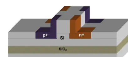
Inthispaper,thestructureisbasedonaP-I-Nlateraloptical phasemodulatorfabricatedonsilicon-on-insulator(SOI)substrate [9].ThemodelsweredevelopedusingtheAthenaandDevedit mod-uleinSilvaco.Thefabricationprocessesbeginwiththeformation oftheSOI layer.Then, thesilicon layeris lightlydopedwith a backgroundconcentrationof1×1014cm−3.Theribwaveguideis formedusingtheetchingprocesswhereanoxidelayerisusedasa mask.Theribheightandwidthforthewaveguidestructure spec-ifiedtoobtainsinglemodebehavior.Theribstructureisdesigned tohave0.46minslabheight(h)and0.4minribwidth(W).
Theactiveareaofp-i-ndiodestructurewasfabricatedthroughthe ionimplantationprocesswhereboththep+ andn+ regionwere implantedwithboronandphosphorusrespectively.Thep+ type regionwasdopedwithboronconcentrationof5×1019cm−3ation
Fig.1. Thefirststructurewithonepairofwellsnexttothewaveguiderib.
Fig.2. Thesecondstructurewithtwopairsofwellsnexttothewaveguiderib.
implantationenergyof10keVandannealingtemperatureof600◦C.
Whilethen+ typeregionwasdopedwithphosphorous concen-trationof5×1019cm−3ationimplantationenergyof30keVand annealingtemperatureof600◦C.Finally,themetallizationprocess
wasdonetoformtheelectrodesofanodeandcathode.
ThreedifferentstructuresofSOIphasemodulatorweredesigned andstudiedinthiswork.Inthefirststructure,onlyonepairofp+ andn+wellsexistedadjacenttothewaveguideribasshownin Fig.1.Fig.2showsthesecondstructurewhere2pairsofwellswere placedattheregionnexttotheribwaveguide.Finallyinthethird structureasshowninFig.3,inadditiontothetwopairsofwells,an additionaltwopairsofdopedwellswereplacedonthewaveguide rib.
4. Resultsanddiscussion
Priortoelectricalcharacterization,theopticalanalysiswas car-ried out by using FDTD simulation to ensure the single mode behavioroftheproposeddevice.Fig.1showstheTE fundamen-talmodeprofileoftheproposeddeviceatwavelength1.55m.It
isproventhatthesinglemodebehaviorwasobtainedascalculated (Fig.4).
Theperformanceof thesiliconphase modulatorswere eval-uatedbyvaryingthepositionsofthen+ andp+dopingregions. Theeffectofdopingregionspositionwillbeinvestigatedbased ontotalfreecarrierconcentration,refractiveindexchange,free carrierabsorptionloss,sizeandthemodulationefficiencyofthe modulators.
Fig.5 shows the carrier concentrationof free electrons and holesofthethreedifferentstructuresofmodulatorswhenspecific
Pleasecitethisarticleinpressas:B.Mardiana,etal.,AnalysesforvariousdopingstructuresofSOI-basedopticalphasemodulatorusingfree carrierdispersioneffect,Optik-Int.J.LightElectronOpt.(2013),http://dx.doi.org/10.1016/j.ijleo.2013.09.050
ARTICLE IN PRESS
GModelIJLEO-53972; No.ofPages4
B.Mardianaetal./Optikxxx (2013) xxx–xxx 3
Fig.4. Totalfreecarrierconcentrationagainstappliedvoltage.
Fig.5. Totalfreecarrierconcentrationalongx-axis.
voltageisapplied.Themeasurement offreeelectronsandholes wastakenalongxaxisfromx=1.75tox=2.15whichistheareaof opticalmodepropagateinthedevice.Itisclearlyseenthat struc-ture1andstructure3gavehigherdensityoffreecarriercompareto structure2.Thishappenedduetointerdigitateddopingpositionof p+dann+regioninstructure2andstructure3causefreeelectrons andholestomoveinmanydirectionsinsteadofonedirectionas instructure1.Therefore,theexistingoffreeelectronsandholesin theopticalmodeguidingregionarereducing.Theresultsproofthat theconcentrationofexistingfreecarrierintheactiveregioncanbe manipulatedbythepositionofdopingregionn+andp+.Thus,the determinationofdopingpositionsareveryimportantindesigning theP-I-NSOIphasemodulatorbecauseitwillinfluencetheway howthefreeelectronsandholesmoveintheactiveregionofthe device.
Fig.6shows therelationshipbetweendrivevoltageandthe refractiveindexchange(n)at1.55mwavelength.Ingeneral,
thetotalrefractiveindexchange(n)increasesastheapplied volt-ageishigher.Forinstanceinstructure1,byvaryingtheapplied voltagefrom0.7Vto1Vcausedalmost0.005changesinrefractive indexofthewaveguide.Thishappenedduetomoreinjectedfree holesandelectronsmovedfromthedopingregiontotheoptical guidanceareawhenmoreappliedvoltagewassupplied.Thus,this scenariocausestheincreaseinthefreecarrierdensityand result-ingimprovementofrefractiveindexchange(n)intheguidance regionofthedevice.Itisfoundthat,thestructure1hasthelargest effectontherefractiveindexchange(n),followedbythestructure 3andthestructure2.
Fig.6.Refractiveindexchangeforphasemodulatorswithvariouswaveguide struc-tures.
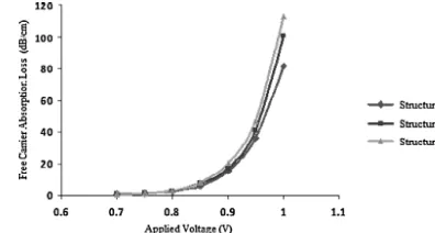
Fig.7. Freecarrierabsorptionlossforphasemodulatorswithvariouswaveguide structures.
Table1
Modulationefficiencyandlengthofmodulator.
Structure 1 2 3
Length(cm) 0.0155 0.0261 0.0205
ModulationEfficiency(Vcm) 0.013 0.023 0.018
Fig. 7 shows the comparison of the absorption lossesvalue withvariousstructureofSOIP-I-Nphasemodulators.Theresults indicated that, upon increasing the drive applied voltage, the absorptionlossincreasedgradually.Structure1producedhighest freeabsorptionlosscomparedtostructure2andstructure3.Even thoughstructure1isproventohavethehighestrefractiveindex change(n)intheprevioussectionbutthisstructureissuffering frombiggestabsorptionloss(˛).Therefore,inseekingabalanced responsebetweenthehighrefractiveindexchangeandlowfree carrierabsorptionloss,adesigntradeoffbetweenthetwoisneeded inordertoproduceagoodSOIphasemodulator.
Table1showsthecomparisonofestimatedlengthandthe mod-ulationefficiency.Themodulationefficiencyisaveryimportant parameterforcharacterizingthemodulatorperformanceandits valuecanbedeterminedbyoverlapping themodulationregion withtheopticalfield.Theoptimizedinteractivelengthofvarious structuresofphasemodulatorsinvestigatedinthisworkisobtain fromthevalueofrefractiveindexchange(n)inFig.6and calcu-latedfromEq.(9).Themodulationefficiencycanbepredictedby FigureofMerit(FoM)VL,whereVisthevoltagetoachievea
phaseshift.ThelowerthevalueofthisFoM,themoreefficientthe modulatoris.Resultshowsthatasmallestdevicecanberealized withstructure 1andresultingthebestmodulationefficiencyof 0.00018Vcm.Asacomparison,themodulationefficiencyof struc-ture1is50%betterthanstructure3%and82%betterthanstructure 2.
5. Conclusion
TheSOIphasemodulatorsbasedonP-I-Ndiodestructurehas beenmodeledusinga3DSILVACOsimulationpackage.Wehave analyzedtheperformanceofmodulatorswithvariousstructureof dopingpositions.Wehaveshownthatdopingpositionsofn+andp+ canbeusedtomanipulatethedensityoffreeelectronsandholesin adevice.Inseekingabalancedresponsebetweenthehighrefractive indexchangeandcarrierabsorptionloss,adesigntradeoffbetween thetwoisneededtobetakenintoconsiderationdependingonthe applicationofthemodulator.
Acknowledgments
Pleasecitethisarticleinpressas:B.Mardiana,etal.,AnalysesforvariousdopingstructuresofSOI-basedopticalphasemodulatorusingfree carrierdispersioneffect,Optik-Int.J.LightElectronOpt.(2013),http://dx.doi.org/10.1016/j.ijleo.2013.09.050
ARTICLE IN PRESS
GModelIJLEO-53972; No.ofPages4
4 B.Mardianaetal./Optikxxx (2013) xxx–xxx
References
[1]A.S.Liu,L.LiO,D.Rubin,H.Nguyen,B.Ciftcioglu,Y.Cherit,N.Izhaky,M.Panicia, High-speedopticalmodulationbasedoncarrierdepletioninasilicon wave-guide,Opt.Express15(2007)660–668.
[2]C.A.Barrios,M.Lipson,Electricallydrivensiliconresonantlightemittingdevice basedonslot-waveguide,J.Appl.Phys.96(2005)6008–6015.
[3]C.E.Png,S.P.Chan,S.T.Lim,G.T.Reed,OpticalphasemodulatorsforMHzand GHzmodulationinsilicon-on-insulator(SOI),J.LightwaveTechnol.22(2004) 1573–1582.
[4]C.Li,L.Zhou,A.W.Poon,Siliconmicroringcarrier-injection-based modula-tors/switcheswithtunableextinctionratiosandOR-logicswitchingbyusing waveguidecross-coupling,Opt.Express15(2007)5069–5076.
[5]G.T.Reed,A.P.Knights,SiliconPhotonics–AnIntroduction,JohnWiley&Sons, UK,2004.
[6]F.Y.Gardes,D.J.Thomson,N.G.Emerson,G.T.Reed,40Gb/ssiliconoptical mod-ulators,Opt.Express12(2011)11804–11813.
[7]H.Xu,X.Xiao,X.Li,Y.Hu,Z.Li,T.Chu,Y.Yu,J.Yu,Highspeedsilicon Mach-ZehndermodulatorbasedoninterleavedPNjunctions,Opt.Express20(2012) 15093–15099.
[8]B.Mardiana,A.R.Hanim,H.Hazura,S.Shaari,P.S.Menon,H.danAbdullah, ActiveSOIopticalring basedonfreecarrierinjection,J.Adv.Mater.Res. 403–408(2012)758–761.
[9]M.Ziebell,D.M.Morini,G.Rasigade,J.M.Fédéli,P.Crozat,E.Cassan,D. Bou-ville,L.Vivien,High-speedringresonatorsiliconopticalmodulatorbasedon interleavedPNjunctions,Opt.Express20(2012)10591–10596.