EFFECT OF DIFFERENT DOPING CONCENTRATION FOR PN CARRIER DEPLETION SILICON-ON-INSULATOR (SOI) OPTICAL MODULATOR
NURHASLINDA BINTI MUSTAFFA KAMAL
This Report Is Submitted In Partial Fulfillment Of Requirements For The Bachelor Degree Of Electronic Engineering (Computer Engineering)
Fakulti Kejuruteraan Elektronik dan Kejuruteraan Komputer Universiti Teknikal Malaysia Melaka
UNIVERSTI TEKNIKAL MALAYSIA MELAKA
FAKULTI KEJURUTERAAN ELEKTRONIK DAN KEJURUTERAAN KOMPUTER
BORANG PENGESAHAN STATUS LAPORAN
PROJEK SARJANA MUDA II
Tajuk Projek : Effect Of Different Doping Concentration For Pn Carrier Depletion Silicon-On-Insulator (SOI) Optical Modulator
Sesi
Pengajian : 1 4 / 1 5
Saya NURHASLINDA BINTI MUSTAFFA KAMAL
mengaku membenarkan Laporan Projek Sarjana Muda ini disimpan di Perpustakaan dengan syarat-syarat kegunaan seperti berikut:
1. Laporan adalah hakmilik Universiti Teknikal Malaysia Melaka.
2. Perpustakaan dibenarkan membuat salinan untuk tujuan pengajian sahaja.
3. Perpustakaan dibenarkan membuat salinan laporan ini sebagai bahan pertukaran antara institusi pengajian tinggi. 4. Sila tandakan ( √ ) :
SULIT*
*(Mengandungi maklumat yang berdarjah keselamatan atau kepentingan Malaysia seperti yang termaktub di dalam AKTA RAHSIA RASMI 1972)
TERHAD** **(Mengandungi maklumat terhad yang telah ditentukan oleh
organisasi/badan di mana penyelidikan dijalankan)
TIDAK TERHAD
Disahkan oleh:
__________________________ ___________________________________
(TANDATANGAN PENULIS) (COP DAN TANDATANGAN PENYELIA)
iii
“I hereby declare that this report is the result of my own work accept for quotes as cited in the reference.”
Signature : ………...
Author : Nurhaslinda binti Mustaffa Kamal
iv
“I hereby declare that I have read this report and in my opinion this report is sufficient in terms of the scope and quality for the award of Bachelor Degree of
Electronic Engineering (Computer Engineering).”
Signature : ………
Author : Dr. Hanim binti Abdul Razak
v
vi
ACKNOWLEDGEMENT
All praise to Allah for my good health and well being. Without His permission, I won’t be able to finish my journey until now.
First and foremost, I wish to express my sincere thanks to my supervisor, Dr. Hanimbinti Abdul Razak. I am very thankful and indebted to her for sharing knowledge, sincerely guide me through the final year and encouraging me to finish the final year project.
I would like to express my special thanks to all my friends that have been such caring to me. They are always sharing important information and remind me when I was forgetting.
vii
ABSTRACT
viii
ABSTRAK
ix
TABLE OF CONTENT
CHAPTER CONTENT PAGE
PROJECT TITLE
REPORT STATUS VERIFICATION FORM
VERIFICATION SSUPERVISOR VERIFICATION DEDICATION ACKNOWLEDGEMENT ABSTRACT ABSTRAK
TABLE OF CONTENT
LIST OF TABLES
LIST OF FIGURES
LIST OF APPENDIX
x
1 INTRODUCTION
1.1 Project Introduction 1.2 Problem Statement 1.3 Objectives
1.4 Scope Of Project 1.5 Report Structure
2 3 3 4 4
2 LITERATURE REVIEW
2.1 Silicon-On-Insulator (Soi) 2.2 SOI Optical Modulator 2.3 Doping Process
2.4 Reverse Bias Pn Carrier
2.5 SOI Optical Modulator Mechanism
6 9 10 14 16
3 METHODOLOGY
3.1 Methodology Flowchart 3.2 Designing The Design 3.3 Analyzing The Result
xi
4 RESULTS AND DISCUSSIONS
4.1 The Structure Of The Device
4.2 Electron And Hole Concentration Reading 4.3 Change Of Refractive Index
4.4 Change Of Absorption Loss
23 27 29 31
5 CONCLUSIONS
5.1 Conclusion 5.2 Recommendation
33 34
REFERENCES 35
xii
LIST OF TABLES
NO TITLE PAGES
xiii
LIST OF FIGURES
NO TITLE PAGES
1 Silicon On Insulator layers 2
2 Ball-and-stick model of the unit cell of silicon [15] 6
3 SOI on chip [4] 7
4 Steps of making SOI wafer [5] 8
5 Electro-optic modulator [9] 9
6 SIMOX fabrication [11] 11
7 The first structure [15] 13
8 The second structure [15] 13
9 The third structure [15] 14
10 Reverse bias energy diagram [16] 15
11 The methodology flowchart 19
12 Structure of SOI optical modulator PN junction 21 13 Set the cutline for the electron and hole concentration 23
14 The device structure in Material display 25
15 The device structure in Net Doping display. 25 16 The device with 5×1016 cm-3 of doping concentration 26
xiv
18 Electron and hole concentration at 0 V 28
19 Electron and hole concentration at -0.75 V 29
xv
LIST OF APPENDICES
NO TITLE PAGE
CHAPTER 1
INTRODUCTION
2
1.1 Project Introduction
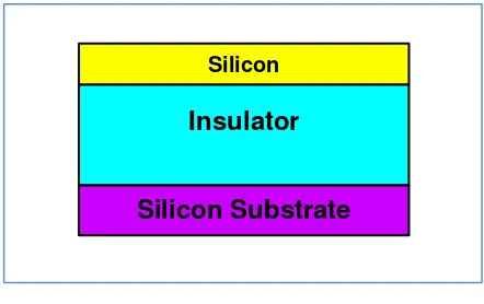
[image:17.612.208.429.247.386.2]Silicon-on-insulator (SOI) is a semiconductor that consists of the layers of a silicon, insulator and silicon substrate. Figure 1 shows the SOI structure that is layered with a thin silicon, insulator and silicon substrate. Recently, SOI is one of the trending technology that is widely used to fabricate optoelectronic devices due to high index contrast between the silicon core and the silica cladding. It is also becoming popular as it is cheap and demonstrates very good performance.
Figure 1 Silicon On Insulator layers
The application of silicon in modulator has been discovered ever since the research of using Silicon in the photonic circuit. In the mid-1980s, they have been studied the Si photonic circuit as the initial work on the fundamental waveguide technology and it is showed that the silicon is a feasible device to use in semiconductor field [1].
Optical modulator will modulate data into light. The outputs that will be exist in this process are the change of refractive index, change of absorption loss and change of phase shift of the light. These outputs can be measured so that the performance can be analyzed.
Silicon
Insulator
3
The doping process is important for semiconductor in order to control their conductivity by adding impurities using ion implantation method. The quantity of determining its concentration and indirectly affects many of its electrical properties. Thus, the performance of carrier depletion SOI optical modulator with various doping concentrations can be investigated.
To investigate the performance, parameters such as the refractive index changes, the absorption loss and the phase shift of the phase modulator can also be compared. The parameters that have been compared are assumed to give result of different performance of the SOI. This project will also produce the structure of PN carrier depletion SOI optical modulator and it is also supplied with reverse supply (reverse bias).
1.2 Problem Statement
The various doping concentrations affect the performance of the SOI optical modulator. Therefore, the analysis of varying different doping concentration on the modulator’s performance should be conducted for guidance in fabrication process.
1.3 Objectives
After completing the project, student will be able to:
Design the PN carrier depletion SOI optical modulator structure using Silvaco Software.
4
1.4 Scope of Project
The Silvaco software is utilized in the project in order to design the optical modulator and it is also involved the Atlas and Athena tools. The Atlas tool is used as the medium to find the refractive index, the absorption loss and the phase shift modulator. While Athena tool is used to design the structure. This device is designed to operate at 1.55 µm optical wavelength.
1.5 Report Structure
CHAPTER 2
LITERATURE REVIEW
Since the first era of research on optical circuits in the 1970s, there have been visions of designing an optical chip that has the capabilities to conduct optical circuit’s behavior. The optical superchip was said to have variety optical components and may carry out modulation, manipulation, light generation, detection and also amplification [1].
In the early phase of optical circuit research, the optical circuit was associated with materials such as lithium niobate (LiNb03) and III-IV semiconductor which are
in a group of ferroelectric material. The characteristics of the material are exhibit, can go over in the range of temperature and have a natural electric polarization. However, the choice to use silicon (Si) as the semiconductor and been widely used in microelectronics, have bring to investigation of silicon photonic circuit [1].
6
2.1 Silicon-on-Insulator (SOI)
[image:21.612.177.461.217.491.2]The fundamental silicon material consists of a crystalline solid that have the arrangement of an atom in repetitive structure. Figure 2 shows the unit cell of the silicon crystal and each sphere represents a silicon atom. The unit cell is duplicated in all three directions that strap together in order to form a silicon crystal structure. Each of the Si atom is also has four closest neighbors [3].
Figure 2 Ball-and-stick model of the unit cell of silicon [15]
7
[image:22.612.147.527.277.545.2]In the manufacturing, there are a few major steps to be done to produce SOI wafer such in the Figure 3. While Figure 4 shows the illustration of step to make the SOI wafer. The silicon wafer is implanted with hydrogen and the hydrogen concentration peaks at some distance below the surface. Then, two wafers are holding each other by the atomic bonding force, upside down. A low temperature annealing causes the two wafers to fuse together. The silicon wafer is then applied with another annealing step that causes the implanted hydrogen to coalesce and form a large number of tiny hydrogen bubbles at the same distance of the peak below the surface. This step will create sufficient mechanical stress to break the wafer at that plane.
8
9
2.2 SOI Optical Modulator
Silicon developments have also continued to grow silicon based technology to improve the frontiers of device integration, complexity and speed. For example, computer and high speed electronics device are the application that is demand in switching field [6].
The other type of semiconductor material such as III-V alloys, it has the characteristics that maintains to be part of the construction of the optoelectronic and a plain photonic device. The relationship of photonics is the technology and the signal generation, processing, transmission and detection is where the signal is carried by light. The examples of photonic devices are such as lasers, waveguides, modulators, detectors and optical fiber [7].
[image:24.612.115.532.442.628.2]The optical modulator is an optoelectronic device that provides modulated optical signal at the output and driven by an electrical command when a continuous input beam is provided at the input. This can be shown in Figure 5 which it is an example of one type of modulator. [8]
![Figure 2 Ball-and-stick model of the unit cell of silicon [15]](https://thumb-ap.123doks.com/thumbv2/123dok/499973.56071/21.612.177.461.217.491/figure-ball-stick-model-unit-cell-silicon.webp)
![Figure 3 SOI on chip [4]](https://thumb-ap.123doks.com/thumbv2/123dok/499973.56071/22.612.147.527.277.545/figure-soi-on-chip.webp)
![Figure 4 Steps of making SOI wafer [5]](https://thumb-ap.123doks.com/thumbv2/123dok/499973.56071/23.612.211.428.68.554/figure-steps-of-making-soi-wafer.webp)
![Figure 5 Electro-optic modulator [9]](https://thumb-ap.123doks.com/thumbv2/123dok/499973.56071/24.612.115.532.442.628/figure-electro-optic-modulator.webp)
