TAGUCHI ANALYSIS ON THE PERFFORMANCE OF CARRIER DEPLETION SOI OPTICAL MODULATOR
NOR FATIHAH BT RAZALI
This Report is submitted in Partial Fulfillment of Requirements for the Bachelor Degree Electronic Engineering (Computer Engineering)
FACULTY OF ELECTRONIC AND COMPUTER ENGINEERING Universiti Teknikal Malaysia Melaka
v
ACKNOWLEDGEMENTS
Assalamualaikum….
All thanks to the Almighty God for his grace and mercy to get me to complete this thesis. Here, I want to give my appreciation and to express my gratitude to my guide Madam Dr Hanim Binti Abd Razak and Madam Dr Hazura Binti Haroon for their guidance, monitoring and encouragement throughout of this thesis.
Apart from that, my completion of this thesis could not have been accomplished without the support of my dearest friend and also my housemate for their help and contribution in any way for this thesis. Hopefully, all flushing that given the knowledge the best possible to take the advantage in seeking blessings.
In addition, thanks a lots to my parents as well because give everything I want and spend a lot of money for me to complete this thesis. Finally, real good comes from God and bad comes from my own.
vi
ABSTRACT
vii
ABSTRAK
ix
3.1 Flowchart methodology 11
3.2 Taguchi method 12
CHAPTER 4: Result and Discussion
4.1 Design of the PIPIN optical modulator 15 4.1.1 Control factor of Concentration of doping 17 4.1.2 Control factor of Voltage 19 4.1.3 Control factor of Energy 21
4.2 Result for Refractive index 23
4.3 Taguchi method 24
CHAPTER 5: Conclusion and Recommendations
5.1 Conclusion 28
5.2 Recommendation 31
References 32
x
LIST OF TABLE
NO Title Page
1.1 L9 Orthogonal Array 2
3.1 Control factor with their level 14
xi
LIST OF FIGURE
NO Title Page
1.1 Structure of SOI PIPIN modulator 2
2.1 Types of optical modulator 5
2.2 Schematic of a Mach- Zender interferometer modulator 7 with two phase shifter sections
2.3 Sketch of the silicon Mach-zehnder modulator on a 7 SOI chip
2.4 Schematic of PIPIN 8
2.5 When applying reverse bias 9
3.1 Flowchart of the project 12
3.2 Step for Taguchi method 13
4.1 SOI PIPIN modulator structure 16
4.2 Doping SOI PIPIN structure 16
4.3 Doping with 5e15cm-3 17
4.4 Doping with 5e17cm-3 18
4.5 Doping with 5e21cm-3 18
4.6 Voltage with -2.94V 19
4.7 Voltage with -2.95V 20
xii
4.9 Energy with 10eV 21
4.10 Energy with 30eV 22
4.11 Energy with 50eV 22
4.12 Factor effect graph for refractive index change 26
4.13 Confirmation test 27
xiii
LIST OF APPENDIX
NO Title Page
1
CHAPTER 1
INTRODUCTION
1.1 Introduction
In this project, Taguchi method was used to optimize the performance of carrier depletion SOI PIPIN optical modulator. Then, this project is focused on optical modulation in silicon on insulator (SOI).
Silicon on insulator (SOI) is comprised of a thin silicon uppermost layer and a thicker silicon lowermost layer with an insulating material like silicon dioxide forming the middle layer between these silicon layers. Subsequently, silicon on insulator (SOI) substrates for silicon photonics provides various benefits like lower energy wastage and low power usage. Silicon is the material which is cheaper and suitable for integrated photonic.[3]
2
Figure 2.1: Structure of SOI PIPIN modulator [5]
This project utilized simulation of ATHENA and ATLAS from Silvaco Int. ATHENA was used to design while ATLAS was used to generate the electrical characteristics.
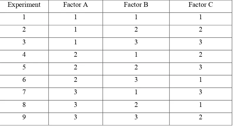
For this project, Taguchi method was applied to optimize the performance. Taguchi method approach a systematic application for designing and analyzing the product quality at the design stage. Then, the L9 orthogonal array was used to find the optimum factors and levels in Taguchi method. Table 1.1 shows that the L9 orthogonal array that contains nine experiments and three factors.
Table 1.1: L9 Orthogonal Array
Experiment Factor A Factor B Factor C
1 1 1 1
2 1 2 2
3 1 3 3
4 2 1 2
5 2 2 3
6 2 3 1
7 3 1 3
8 3 2 1
3
1.2 Problem statement
Engineering designs involve setting values of a large number of decision variables. Then, the optimization of a device is crucial so difficult to optimize the performance. So, statistical tool that is Taguchi method was used. Taguchi method is a structured approach for determining the best performance.
1.3 Objectives
1. To design and simulate SOI PIPIN optical modulator by using ATHENA and ATLAS from Silvaco.
2. To optimize the performance SOI optical modulator by using Taguchi method.
1.4 Scope
1. This project is conducted by using Silvaco simulation tools which is ATHENA and ATLAS. The wavelength involved is 1.55µm.
2. This project in focused to optimize the performance of carrier depletion SOI PIPIN optical modulator by using Taguchi method.
1.5 Project Outline
4
CHAPTER 2
LITERATURE REVIEW
2.1 Optical modulator
5
Figure 3.1: Types of optical modulator [1]
2.2 Silicon on Insulator (SOI)
Silicon-On-Insulator (SOI) is a semiconductor manufacture methods produced by IBM, which employs pure crystal silicon and silicon oxide for integrated circuits (IC) and microchips. Silicon on Insulator (SOI) microchip processing speed is normally thirty percentage faster compared today's complementary metal-oxide semiconductor (CMOS) based chips and power consumption is reduced by eighty percentaege, which makes them suited for cellular devices. SOI chips also reduce the soft error rate, which is data corruption caused by cosmic rays and natural radioactive background signals. [3]
6
Currently, the application of optical data are usually in long distance communications. These connections form the backbone of the communications infrastructure for their ability to send substantial amounts of data at the quikest rate probably. Commonly, the materials of the kind of optical devices developed result in larger costs. The existing technology using electrical signals transmitted along copper wires to transfer data between high-speed fiber optic connection and user using the data that is being transfer.. Unfortunately, method to send large amounts of data is to use an electrical signal which has a lot of connections and achieve the best performance of copper.
The aim of the research in the silicon photonics field is to develop optical devices based on silicon material. This method looks extremely attractive due to several causes, including the large established silicon fabrication infrastructure and the somewhat inexpensive and the material is high.
2.2.1 Mach- Zehnder Modulator
7
Figure 2.2: Schematic of a Mach- Zender interferometer modulator with two phase shifter sections [1]
Mach-Zehnder Interferometers utilized in a wide variety of applications within optics and optical communications. A Mach-Zehnder modulator is utilized for controlling the amplitude of an optical wave. The input waveguide is divided into two waveguide interferometer arms. When a voltage is applied across one of the arms, a phase shift is induced for the wave passing through that arm. When the two arms are recombined, the phase difference between the two waves is converted to an amplitude modulation. Figure 2.3 shows that the brief pieces associated with silicon photonic-crystal nanostructures are incorporated in the two arms of the MZI to alter the phase of the light. One arm is controlled by the exterior oscillating electrical signal applied across two electrodes so that the phase of light is modulated in time. When light from the two arms combines at the exit of the MZI, the time-varying phase of one arm brings the combined light intensity to undulate. [4]
8
According to Graham T. Reed and et al[5] when large refractive index, light can be mostly restricted in submicron waveguide between silicon and buried silicon oxide. Apart from that, a high performance optical modulator should demonstrate low insertion loss, large extinction ratio and high frequency operation.
2.3 Carrier Depletion
Generally, carrier depletion operated in a reverse bias. Figure 2.4 shows that the schematic of PIPIN. The PIPIN diode is the best compromise for high speed and low insertion loss. P-doped region is introduced as a source of free holes in the core of the intrinsic region of the diode. At balance, when a reverse bias was applied the holes that are located in the middle of the diode will be holes out by the electric field as shown as figure 2.5. Changes in the refractive index are then obtained in the middle of the diode. Apart from that, the reverse current flows very slightly even in the reverse bias state in an actual diode. This electric current is called the leakage current or the drift current. In addition, when reverse bias increases, the zener breakdown and the current flow rapidly. The voltage that starts this breakdown phenomenon is called reverse direction breakdown voltage. Moreover, the areas in which the reverse current rapidly increases by the breakdown phenomenon is called breakdown areas. In the breakdown areas, the voltage change becomes small compared with the current change.
9
Figure 2.5: When applying reverse bias
According to Delphine Marris-Morini and et al[12] the carrier depletion can be obtained in the reverse biased PIPIN diode with a P-doped region introduced as a source of free holes in the core of the intrinsic region of the diode. In the balance, holes are placed in the middle of the diode and holes are swept out when a reverse bias is applied by the electrical field. Then, the carrier depletion appears as one of the most efficient ways to achieve high speed and high performance optical modulators. In addition, the PIPIN seems to be more flexible with the possibility to achieve targeted specifications, especially on optical loss and cutoff frequency.
Laurent Vivien and et al[13] do the paper about the optical modulation by carrier depletion in a silicon PIN diode. When in balance, in the P+ layer have localize holes that are electrostatically. Apart from that, when a reverse bias voltage was applied to the diode, expands through the space charge of the device. Then, holes are swept out from the active area. In addition, carrier density variations are responsible for refractive index variations, and thus for a phase shift of the optical guided mode propagating through the device.
2.4 Taguchi Method
10
sensitive to variations in factors such as materials, manufacturing equipment, workmanship and operating conditions.
In addition, Taguchi method is a standardized approach for determining the best combination of inputs to produce a product or service that is based on a Design of Experiments (DOE) methodology for determining parameter levels. DOE is an important tool for designing processes and products. [12]
Pursuant to P.S. Menon and et al[9] the optimizing PIN photodiode using Taguchi method. The four factors which are the intrinsic region length, photoabsorption layer thickness, incident optical power and bias voltage. Then, to examine the performance factors of the device and to find the optimum factors and levels, signal to noise ratio (SNR) of larger the better (LTB) was applied. The result show that the most effect is incident optical power followed by bias voltage, photoabsorption layer thickness and incident optical power.
Other than that, the selected factors that provide the best combination based on L9 orthogonal array and the signal to noise ratio (SNR) larger the best (LTB) is used to find the optimum factors and levels in Taguchi method. Generally, there are three categories of the performance characteristics to analyse the S/N ratio that is nominal the best, larger the better and smaller the better.
11
CHAPTER 3
METHODOLOGY
3.1 Flowchart Methodology
![Figure 2.2: Schematic of a Mach- Zender interferometer modulator with two phase shifter sections [1]](https://thumb-ap.123doks.com/thumbv2/123dok/496896.55444/20.595.189.456.71.187/figure-schematic-mach-zender-interferometer-modulator-shifter-sections.webp)
