OPTIMIZATION OF THE FABRICATION PROCESS PARAMETERS OF AN OPTICAL MODULATOR
MOHAMMAD AZWAN SAFWAN BIN HARUN
This Report Is Submitted In Partial Fulfilment of Requirements for the Bachelor Degree of Electronic Engineering (Computer Engineering)
Fakulti Kejuruteraan Elektronik dan Kejuruteraan Komputer Universiti Teknikal Malaysia Melaka
v
vi
ACKNOWLEDGEMENT
Praise to Allah S.W.T for helping me to get an idea and give me strength to overcome all the difficulties and letting me to finish my Final Year Project I and Final Year Project II. Next, I would like to thank to my beloved and respected supervisor Dr. Hazura Binti Haroon for all the guidance and motivation she gave to me during the process of the project. Without her support, I will not be able to achieved the goals of the project and also difficult to complete my thesis.
vii
ABSTRACT
viii
ABSTRAK
ix
TABLE OF CONTENT
CHAPTER TITLE PAGE
Project Title i
Confirmation Report Status ii
Declaration iii
Approval iv
Dedication v
Acknowledgement vi
Abstract vii
Abstrak viii
Table of Content ix
List of Tables xi
List of Figures xiii
List of Appendix xvi
List of Abbreviation xvii
1 INTRODUCTION 1
1.1 Introduction 1
1.2 Problem Statement 3
1.3 Objective of Project 4
1.4 Scope of Project 4
1.5 Important of Project 4
1.6 Project Outline 5
2 LITERATURE RIVIEW 6
2.1 Optical Modulator 6
2.2 The Silicon Waveguide Structure 7
2.3 The Fabrication Process 8
2.4 Material Element for The Doping 14
x
2.6 Taguchi Method 18
3 METHODOLOGY 20
3.1 Modelling/Creating Silicon Fabrication 20
3.2 Optimization Process 22
3.3 The Taguchi Method 23
4 RESULTS AND DISCUSSIONS 26
4.1 The Fabrication Process Modelling 26
4.2 The Optimization Process 30
4.2.1 Experiment A 31
4.2.2 Experiment B 40
4.2.3 Experiment C 49
4.2.4 Experiment D 58
4.3 Conclusion 67
5 CONCLUSION AND RECOMMENDATION 68
5.1 Conclusion 68
5.2 Recommendation 69
xi
LIST OF TABLES
NO TITLE PAGE
2.1 Boron properties. 14
2.2 Phosphorus properties. 15
2.3 Aluminium properties. 15
2.4 Arsenic properties. 16
2.5 The L9 orthogonal array in Taguchi Method. 19
3.1 Experiment A with control factor with their levels. 24 3.2 Experiment B with control factor with their levels. 24 3.3 Experiment C with control factor with their levels. 25 3.4 Experiment D with control factor with their levels. 25 4.1 The parameter control factor of Experiment A. 31 4.2 Taguchi L9 orthogonal array shown for Experiment A. 32
4.3 The results of modulation efficiency. 34
4.4 The results of absorption loss. 37
4.5 The parameter control factor of Experiment B. 40 4.6 Taguchi L9 orthogonal array shown for Experiment B. 41
4.7 The results of modulation efficiency. 43
4.8 The results of absorption loss. 46
4.9 The parameter control factor of Experiment C. 49 4.10 Taguchi L9 orthogonal array shown for Experiment C. 50
4.11 The results of modulation efficiency. 52
4.12 The results of absorption loss. 55
4.13 The parameter control factor of Experiment D. 58
xii
4.15 The results of modulation efficiency. 61
4.16 The results of absorption loss. 64
xiii
LIST OF FIGURES
NO TITLE PAGE
1.1 p-i-n junction of an injection-type modulator. 2 1.2 SOI Mach Zehnder interferometer with an optical modulator. 2 2.1 MOS capacitor of an accumulation-type modulator. 7 2.2 The silicon waveguide with p-i-n diode structure integrated on SOI. 7
2.3 The dry etching process. 9
2.4 The fabrication of silicon optical waveguide. 9 2.5 The epitaxial growth process. 10
2.6 The oxidation process. 10
2.7 Photosensitive liquid photoresist layer. 11
2.8 Align mask. 11
2.9 The expose pattern and hard bake. 11
2.10 A solution of hydrofluoric acid. 12
2.11 The etching windows in barrier layer. 12
2.12 Remove photoresist. 12
2.13 Diffusion process. 13
2.14 Ion implantation process. 13
3.1 The flow of modelling or creating silicon fabrication. 21
3.2 Optimization process. 22
3.3 Steps for Taguchi method. 23
4.1 Bare silicon. 27
4.2 Silicon rib waveguide 27
4.3 Oxide deposition 27
4.4 Etch left side of oxide. 27
xiv
4.6 Etch all side of oxide. 28
4.7 Oxide deposition. 28
4.8 Etch right side of oxide. 28
4.9 Doped boron concentration. 29
4.10 Etch both side of oxide 29
4.11 Oxide deposition. 29
4.12 Etch both side of oxide. 29
4.13 Apply aluminium. 29
4.14 Etch aluminium and oxide. 29
4.15 Injecting Vanode 30
4.16 One of the results of silicon from Experiment 9 in Experiment A. 33
4.17 The concentration of electron and hole at 0V and 0.7V. 33
4.18 The modulation efficiency with the four parameters variation. 35
4.19 The graph of signal noise ratio. 35
4.20 The data of the Taguchi analysis of modulation efficiency. 36
4.21 The absorption loss with the four parameters variation. 38
4.22 The graph of signal noise ratio. 38
4.23 The data of the Taguchi analysis of absorption loss. 39
4.24 One of the results of silicon from Experiment 9 in Experiment B. 42
4.25 The concentration of electron and hole at 0V and 0.7V. 42
4.26 The modulation efficiency with the four parameters variation. 44
4.27 The graph of signal noise ratio. 44
4.28 The data of the Taguchi analysis of modulation efficiency. 45
4.29 The absorption loss with the four parameters variation. 47
4.30 The graph of signal noise ratio. 47
4.31 The data of the Taguchi analysis of absorption loss. 48
4.32 One of the results of silicon from Experiment 9 in Experiment C. 51
4.33 The concentration of electron and hole at 0V and 0.7V. 51
4.34 The modulation efficiency with the four parameters variation. 53
4.35 The graph of signal noise ratio. 53
4.36 The data of the Taguchi analysis of modulation efficiency. 54
4.37 The absorption loss with the four parameters variation. 56
xv
4.39 The data of the Taguchi analysis of absorption loss. 57
4.40 One of the results of silicon from Experiment 9 in Experiment D. 60
4.41 The concentration of electron and hole at 0V and 0.7V. 60
4.42 The modulation efficiency with the four parameters variation. 62
4.43 The graph of signal noise ratio. 62
4.44 The data of the Taguchi analysis of modulation efficiency. 63
4.45 The absorption loss with the four parameters variation. 65
4.46 The graph of signal noise ratio. 65
xvi
LIST OF APPENDIX
NO TITLE PAGE
A Simple Modelling Coding 72
xvii
LIST OF ABBREVIATION
PIN – Positive-Intrinsic-Negative SOI – Silicon – On – Insulator UV – Ultraviolet
CMOS – Complementary metal–oxide–semiconductor MOS – Metal–oxide–semiconductor
1
CHAPTER 1
INTRODUCTION
1.
The introduction of the project discussed in this chapter includes the problem statement, the main objective and the scope of the project. The important of the project is described based on the sustainable development and potential commercialization.
1.1 INTRODUCTION
2
[image:19.595.250.424.240.374.2]which requires the resistive contacts (highly doped regions) to be only a few hundred nanometers away from each other to avoid limiting the bandwidth and Figure 1.2 shows the Silicon-On-Insulator (SOI) Mach Zehnder interferometer with an optical modulator [2]. The high-speed interferometers based on concept with a bandwidth of 1GHz were first proposed in 2004, followed in 2005 by a design featuring a much reduced waveguide size and significant bandwidth increase (24GHz), achieved by insertion of ”lifetime killers” (impurities) in the waveguide area.
Figure 1.1: p-i-n junction of an injection-type modulator.
Figure 1.2: SOI Mach Zehnder interferometer with an optical modulator.
[image:19.595.247.430.428.526.2]3
project. The silicon in microelectronics field has been important and preferable based on its performance or capability. The capability to combine with low cost raw materials, simple processing and useful temperature range has made it as the one of the best materials among the others. Also, the improvement and development of technologies has increase the advancement and the efficiency of the cost of the silicon based fabrication technology.
The project involved the process of modelling and optimizing the fabrication process of an optical modulator by using Silvaco software. By using Athena from Silvaco software, it provides us with all the process needed in wafer fabrication such as oxidation, lithography and etching process. For this project, the optimization will focus on the fabrication parameters such as oxidation time, resist stripping time, ultraviolet (UV) exposure time and others to meet the stringent requirements in the actual fabrication process [3]. The dry etching process is selected in the etching process, in order to evaluate the effect of etching techniques on the waveguide structure. The project involved diffusion of N-type and P-type materials waveguide structured with the silicon orientation of <100>. Besides that, the optimization will be carried out by the Taguchi method. The Taguchi method is the technique to reduce the variation in a process throughout tough design of experiment and this method is capable to produce a good quality of product at a lower cost. Therefore, the research on development and the process of fabrication cost time can be further reduced.
1.2 PROBLEM STATEMENT
4
to produce a good quality of product at a lower cost. Therefore, the project should be cutting the costs and the researches of development time can be further reduced.
1.3 OBJECTIVES OF PROJECT
The main objective of this project is to optimize the fabrication process parameter of an optical modulator. The goals of this project are;
To model simple, cost-effective and scalable fabrication process of an optical modulator by using Silvaco software.
To investigate the influence of fabrication parameter variations on optical modulator performance.
To obtain the optimal fabrication process of an optical modulator by using Taguchi method.
1.4 SCOPE OF PROJECT
The scope of this project is to model an optical modulator by using Silvaco software simulation tools. The silicon orientation of <100> is considered. Silvaco software simulation tools is employed in the fabrication modelling and taking into account the phosphorus diffusion temperature, boron diffusion temperature, silicon orientation and oxide thickness. The simulation modelling is important to estimate the optimum fabrication parameters in order to meet the stringent requirements in the actual fabrication process. The dry etching was selected for the etching process in the fabrication process. The p-i-n diode structure is choose to be operated at λ =1.55 optical wavelength. Besides that, the Taguchi method will be used for the silicon parameter optimization.
1.5 IMPORTANT OF PROJECT
1.5.1 Sustainable Development
5
the designer can test the fabrication process and analyze the result without having to create or fabricate the actual silicon wafer and this will give a lot of benefits for the designers or for the industry in terms of reduced fabrication times and costs. The optimizing of the fabrication process is not applied on optical modulator, but can also be accounted for any of waveguide based on optical devices. Example: waveguide filter, switching, amplification, multiplexing and etc.
1.5.2 Potential Commercialization.
The project potential commercialization is aimed to be implemented in the sectors of microelectronics, microphotonics or semiconductor devices. In addition, this project can been further implemented in the industry company such as in telecommunication companies.
1.6 PROJECT OUTLINE
6
CHAPTER 2
LITERATURE REVIEW
2.
The literature review on the project will briefly discussed based on theoretical, background knowledge and methodological approaches in silicon waveguide fabrication.
2.1 OPTICAL MODULATOR
7
[image:24.595.219.457.189.347.2]integrated circuits with a high level of functionality. For example, Figure 2.1 shows the Metal-oxide-semiconductor (MOS) capacitor-type modulators are accumulation devices in which only majority carriers are accumulated on both sides of an insulating layer of silicon dioxide. This layer, placed in the wave guiding region, limits the bandwidth of the device to the resistance-capacitance cut-off frequency [2].
Figure 2.1: MOS capacitor of an accumulation-type modulator.
2.2 THE SILICON WAVEGUIDE STRUCTURE
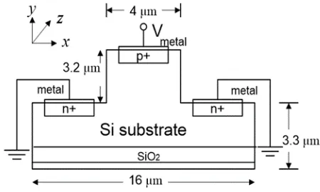
In the silicon photonic, there are a lot of applications silicon waveguides types that can be chosen. For example, rib waveguide, hollow-core waveguide, free standing waveguide and etc. Apart from that, many materials can be used to realize a waveguide on silicon such as silicon dioxide, silicon oxynitride, polymers, phosphorus, boron and the silicon itself. A rib structures exist on the top layer of the silicon acts as guidance to guide the optical power in the silicon plane. Figure 2.2 shows an example of the silicon optical waveguide structure [4].
[image:24.595.222.447.601.736.2]