ICSE2010 Proc. 2010, Melaka, Malaysia
An Analysis of Silicon Waveguide Phase Modulation
Efficiency based on Carrier Depletion Effect
Hazura H., Hanim A.R, Mardiana B. and Menon, P.S.,
Member, IEEE
Institute of Microengineering and Nanoelectronics Universiti Kebangsaan Malaysia
43600 Bangi, Selangor, MALAYSIA
Email: [email protected], [email protected], [email protected], [email protected]
Abstract- This paper highlights the study of carrier depletion effect on silicon waveguide with p-i-n diode and NPN structure. The device performance is predicted by using 2D Silvaco CAD software under different applied voltages. Device performances in terms of modulation efficiency will be discussed.
I. INTRODUCTION
SINCE the 1980’s, silicon photonic devices have been extensively studied, however a submicrometre-size photonic devices have been realized only in the last few years. Silicon properties namely the transparency in the range of optical telecommunications wavelengths and high index of refraction, have enabled the fabrication of low loss submicron waveguide. Photonic devices such as splitter, coupler, and filter have been demonstrated in silicon but once the device has been fabricated, the properties of the device are predetermined. A silicon based modulator can be used to control the flow of light, where the refractive index of the silicon waveguide can be varies thus, induce a change in the transmission properties.
A refractive index of a silicon modulator can be physically altered based on free carrier concentration variation. There are several means that can be used to vary the carrier concentration in silicon: injection, accumulation, depletion, or inversion of carrier. In this paper, we investigated the performance of the silicon modulator for carrier depletion based device. Recent works have been focused on designing a smaller and high speed device, while less on the effect of the optical and electrical properties to the design. The fundamentals study based on the device performance is crucial as the motivation for designing high speed and high efficiency photonic device to be integrated in any optoelectronic applications.
II. SILICON MODULATOR DESIGN
To date, several device configurations such as p-i-n diode structure [1,2,3] and, MOS capacitor [4] have been proposed. We studied a micrometer scale silicon modulator based on p-i-n diode ap-i-nd NPN structures to be operated at 1.55µm ap-i-nd 1.3µm optical wavelength.
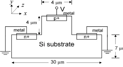
Fig.1(a) Silicon modulator p-i-n structure cross section.
Fig.1(b) Silicon modulator NPN structure cross section.
Fig.1(a)-1(b) show the waveguide cross section of the silicon optical modulator where the modulation acts. The p-i-n and NPN diode configurations have been employed in our design to study the performance of each modulator design.
The P+ type region is implanted with 5x1018 cm-3 Boron concentrations while the N+ type region is phosphorus implanted region with a concentration of 5x1018 cm-3. Both structures have a background doping concentrations of 1x 10¹⁴. For both structure, the depth of the implanted region is about 1.8 m for N+ region and 1.6 m for P+ region. The rib height and width for both structure is chosen in order to have a single mode behavior. The rib structure is designed to have 4 µ m in height and 4 µm in width. With the chosen doping concentrations for both structures, the distance of the doped regions to the rib sidewalls turns to be 1.4 m for the first proposed structure and 1 m for the second structure.
348
ICSE2010 Proc. 2010, Melaka, Malaysia
As mentioned before, in order to alter the refractive index of the silicon waveguide, the free carrier concentrations of the waveguide can be varied by depletion [5,6] or injection [7,8] carrier method. In carrier depletion method, a negative bias is applied to the P electrode which in turns changes the width of the depletion region thus eventually changing the effective refractive index. In contrast, the carrier injection can be obtained with the structure is forward biased. The injected current will proportionally vary the refractive index and optical absorption of the silicon waveguide. Our study will aim only the effect of carrier depletion to the all silicon waveguide.
The optical power of 1mW is applied to our design for both structures and the effect of refractive index variations for 1.55µm and 1.3µ m optical wavelength is investigated.
III. RESULTS AND DISCUSSIONS
The carrier depletion effect on refractive index of a silicon waveguide has been theoretically investigated by using a two dimensional simulation package, Silvaco. We used ATHENA to simulate the device structure while ATLAS to obtain the device characteristics. The important parameters employed in the simulations are shown in Table 1.
The performance of the silicon modulator is evaluated based on the device modulation efficiency. Our study is focuses on the effect of refractive index variations to this parameter due the changes of driving voltage.
Refractive index change in silicon based on free carrier concentration variation can be calculated from the equations derived by R.A Soref [9] from the Drude- Lorenz equations. The equations are:
For o=1.55 :
] (1)
(2) For o=1.3 :
] (3)
(4) where is the refractive index change and and are the electron and hole concentration variations, respectively while is the change in absorption and and are the change in absorption resulting from change in free electron and hole carrier concentrations respectively.
TABLE 1 Simulations Parameters
Si refractive index 3.475 Si background carrier conc. (cm-3) 1x10¹⁴
p 2x10
-6
n 2x10
-6
Temperature (K) 300
Combining the two equations at the specific wavelengths, we can calculate the effective index change of a mode and therefore the resulting phase shift for a given voltage.
By observing the doping concentrations variations at the waveguide center (x=4 m, y=8 m), it enables us to work out for refractive index change for a specific bias voltage and therefore the resulting phase shift and length of the device, where the relationship can be summarized as:
(5) where L is the length of the modulator. For -radian phase shift, the estimated length will be:
(6)
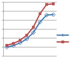
Based on (6), graphs as shown in Fig.2(a) and Fig.2(b) are plotted.
For p-i-n diode structure, between -2 to -8 bias voltage, the estimated modulator length is nearly the same for both 1.55µ m and 1.3 µm wavelength.
For 1.55µm, the predicted length is about 1.52 mm while for 1.3 µm, 1.92mm. The estimated length of the device is dramatically increased when -1 bias is applied where the length is about 2.4 mm for 1.3 µm and 1.88mm for 1.55 µm.
Fig.2(a) Estimated modulator length for p-i-n diode configuration.
ICSE2010 Proc. 2010, Melaka, Malaysia
Fig.2(b) Estimated modulator length for NPN diode configurations.
In contrast, the length of the modulator employing NPN structure decreased linearly with the increase of reverse voltage. With -8 applied voltage, the possible length is about 0.99 mm for 1.55 µm and 1.2 mm for 1.3 µm.
Both results show that a smaller device can be realized if the device is designed to be operated at 1.55 µm compared to 1.3 µ m wavelength. But since the free carrier dispersion effect is relatively weak in silicon, a long device is well expected for both wavelengths.
From (6), it can be seen that the length of the modulator will be shrink as the refractive index variation increased. The phase modulation efficiency of the device can be calculated by V L , where V is the voltage to achieve a phase shift. The simulation shows that with -8 V, the V L of the p-i-n diode modulator is 1.53 Vcm for 1.3 µ m wavelength and 1.22 Vcm for 1.55 µ m. While for NPN configuration, the V L for 1.3 µ m is 0.96 Vcm and 0.8 Vcm for 1.55 µm. Both designs prove that working at wavelength 1.55 µm is suggested to have a device with better phase modulation efficiency.
An improved phase modulation efficiency can be obtained by shorten the device length. This can be made by shrinking the size of the waveguide to a smaller dimensions [10,11,12,13].
IV. CONCLUSIONS
In this paper, we have estimated the theoretical performance of silicon modulator. In our design, carrier depletion is used as one of the most efficient means of implementing optical modulation. For NPN waveguide configurations, the overlapping between the optical mode and the nonequilibrium charge distributions is larger; therefore a smaller device is expected due to higher refractive index change.
Even though simulation shows that the demonstration of a high efficiency silicon modulator looks promising, a real challenge still depends on the fabrication technology.
ACKNOWLEDGMENT
The authors are very grateful to the staff of Photonic Technology Lab, IMEN. The authors also would like to thank UTEM for their support.
REFERENCES
[1] Andrea Irace, Giuseppe Coppola, Mario Iodice, and Antonello Cutolo, “A high-efficiency silicon optoelectronic modulator based on a Bragg Mirror and integrated in a low-loss silicon on insulator waveguide”, Proc. Of SPIE, Vol. 3847, 1999.
[2] D. W Zheng, B. T Smith, J. Dong, and Asghari, “ On the effective lifetime of a silicon p-i-n diode optical modulator”, Semicond. Sci. Technol., Vol. 23, 2008.
[3] C. Z. Zhao, E.K. Liu, G. Z. Li, Y. Gao, and C.S Guo, “Zero-gap directional coupler switch integrated into a silicon- on- insulator for
1.3-m operation”, Opt. Lett., vol.21, no.20, pp.1664,1996.
[4] L.Liao, D. Samara-Rubio, M.Morse, A. Liu, H. Hodge, D. Rubin, U.D Keil, T. Franck, “High Speed silic.on Mach- Zehnder modulator”, Opt. Express 13, pp.3129-3135, 2005.
[5] A. Brimont, F.Y Gardes, P. Sanchis, D. Marris-Morrini, P. Dumon, J.M Fedeli, L. O’Faolin, W. Boagert, L. Vivien, J. Marti, G.T Reed, and T.F. Krauss, “Design of a micro-ring resonator electro-optical modulator embedded in a reverse biased PN junction”, Proc. ECIO, ThD4, pp. 15947- 15958, 2008.
[6] Zhi-Yong Li, Dan-Xia Xu, W. Ross Mc Kinnon, Siegfried Janz, Jens H. Schmid, Pavel Cheben, and Jin-Zhong Yu, “Silicon waveguide modulator based on carrier depletion in periodically interleaved PN junctions”, Optics Express, Vol.17, No.18, pp. 15947-15958, 2009.
[7] Giuseppe Coppola, Iodice Mario, Ivo Rendina, “Analysis of a planar silicon optoelectronic modulator based on the waveguide- vanishing effect”, Proc. Of SPIE, Vol. 6593, 2007.
[8] V. R. Almeida, C. A. Barrios, R.R Panepucci, and M. Lipson, “All-optical control of light on a silicon chip”, Nature, vol.431, no.7012, pp. 1081-1084, 2004.
[9] R.A Soref and B. R Bennett, “Kramers-Kronig analysis of electro-optical switching in silicon”, Proc. SPIE, vol.704, pp.1622-1631, 2004. [10] Delphine Marris-Morrini, Xavier Le Roux, Daniel Pascal, Laurent
Vivien, Eric Cassan, Jean Marc Fedeli, Jean Francois Damlencourt, David Bouville, Jose Palomo, and Suzanne Laval, “High speed all- silicon optical modulator”, Journal of Luminescence, vol. 121, pp.387-390, 2006.
[11] A.Cutolo, M.Iodice, A.Irace, P.Spirito, and Zeni, “An electrically controlled Bragg reflector integrated in a rib silicon on insulator waveguide,” Appl.Phys.Lett., vol.71, no.2, pp.199, 1997. [12] C. Angulos Barrios, V.R Almeida, and M. Lipson,
“Low-power-consumption short-length and high- modulation-depth silicon electro-optic modulator,” J. Lightwave Technol., vol.21, no.4, pp. 1089-1098, 2003.
[13] C. Angulos Barrios, V.R Almeida, R.Panepucci,and M. Lipson, “Electrooptic modulation of silicon-on-Insulator submicronmeter-size waveguide devices”, J. Lightwave Technol., vol.21, no.10, pp. 2332-2339, 2003.