Abstract — This paper presents the study of electrical characteristic of phase modulator in the carrier injection mode. The phase modulator device has been integrated in the silicon-on-insulator (SOI) rib waveguide by using the p-i-n diode structure. The electrical device performance is predicted by using the 2-D semiconductor package SILVACO (CAD) software under DC operation. In summary, the phase modulator device required 0.035mA drive current to get phase shift at wavelength 1.55µm meanwhile 0.066mA drive current is required for the 1.3µm the silicon photonics. Silicon photonics have been intensively studied by many research groups with the intention of linking it between the field of optical communication and the silicon integrated circuits. The performance of the integrated circuit (IC) will be improved by the integrating of the optics and the electronics on the same chip; in which it would benefit the telecommunications application for the development of the low cost solutions for the high-speed optoelectronic devices and systems. There are many benefits of the silicon as a photonic medium [1][3]. Especially, it is transparent in the range of optical telecommunications wavelengths (1.3 and 1.55µm) and because of it high index refraction. Due to its uniqueness characteristic, silicon is very
Manuscript received March 26, 2010. Mardiana B. is with Universiti Teknikal Malaysia Melaka, Locked Bag No.1752, Durian Tunggal Post Office, 76109, Durian Tunggal, Malacca, Malaysia (phone: +60173674795;fax:+6038925809;e-mail:[email protected]).She is currently working towards the PhD degree under the supervision of Prof Shahbudin Saari at the IMEN, Unniversiti Kebangsaan Malaysia.
Hazura H. is with Universiti Teknikal Malaysia Melaka, Locked Bag No.1752, Durian Tunggal Post Office, 76109, Durian Tunggal, Malacca, Malaysia (phone: +601336531205 ;fax:+6038925809;e-mail:[email protected]). She is currently working towards the PhD degree under the supervision of Prof Shahbudin Saari at the same university
Hanim A.R. is with Universiti Teknikal Malaysia Melaka, Locked Bag No.1752, Durian Tunggal Post Office, 76109, Durian Tunggal, Malacca, Malaysia (phone: +60133989002 ;fax:+6038925809;e-mail:[email protected]). She is currently working towards the PhD degree under the supervision of Prof Shahbudin Saari at the same university.
Sahbudin Saari. is with Institute of Microengineering and nanoelectronics, 43600 Bangi, Selangor (phone: +60389216308; fax:+6038925809;e-mail:[email protected]). In 2003, he joined IMEN as Professor and also Principal Fellow works on Photonic Technologies Research and Development.
suitable for the fabrication material of the high-index-contrast sub-micrometer structures [1]. Furthermore, the matured silicon integrated circuit process technology in bipolar and complementary metal–oxide semiconductor provides the breakthrough of the implementation of the dense silicon-based integrated optics and electronics on-chip. Optoelectronic devices such as the modulator and the switch is very much dependable on the plasma dispersion effect and the thermal effects in the silicon. From the previous research, it is proven that the most successful silicon optical modulators are based on the free carrier density. By inducing more free carrier in the guidance region, it will control the optical refractive index xccv bchanges [3,4]. This can be achieve by the doping of the p+ or n+ region nearer the waveguide. Soref and Bennet [7] quantified the changes they had identified from the research for the refractive index and in the absorption coefficents. The following equations are widely used in order to evaluate changes due to injection or depletion of carriers in silicon and hence are utilized in this report: been used in this work is shown in Figure 1. By observing the doping concentrations variations at the waveguide centre (x=4 m, y=8 m), it enable us to work out for the refractive index change for a specific forward bias voltage and therefore the resulting phase shift of the device, in which the relationship can be summarized as:
= 2 nL/ … (3) where L is the length of the modulator. In this work, the length of the modulator is assumed as 500µm.
Phase modulator based on Silicon-on-Insulator
(SOI) rib waveguide
Mardiana B, Hazura H, Hanim AR, Sahbudin Shaari,
Member, IEEE,
Huda Abdullah.
O
ICP2010-55
Figure 1: Cross section of the p-i-n phase modulator.
II. PHASE MODULATOR DESIGN
Recently, several device configurations such as the p-i-n diode structure [6] and, MOS capacitor [10] have been proposed. We studied the micrometer scale silicon modulator based on the p-i-n diode structure to be operated at 1.55µ m and 1.3µm optical wavelength.
The P+ type region is implanted with 5x1018 cm-3 Boron concentrations while the N+ type region is the phosphorus implanted region with a concentration of 5x1018 cm-3. The structures have the background doping concentrations of 1x 10¹⁴. The depth of the implanted region is about 1.8 m for N+ region and 1.6 m for P+ region. The rib height and width of the structure is chosen in order to have a single mode behaviour. The rib structure is designed to have 3.2 µm in height and 4 µ m in width. With the chosen doping concentrations for the structure, the distance of the doped regions to the rib sidewalls turns to be 1.4 m.
The optical power of 1mW is applied to our design of phase modulator and the effect of the refractive index variations for 1.55µm and 1.3µm optical wavelength is investigated. The important parameters used in the simulations are shown in Table 1.
TABLE 1
SIMULATION PARAMETERS
Si refractive index 3.475
Si background carrier conc. (cm-3) 1x10¹⁴
p (s) 2x10
-6
n (s) 2x10⁻⁶
Temperature (K) 300
III. RESULTS AND DISCUSSION
In this work, the active region of the phase modulator have been tested under DC operation. The active device will be operated by applying an external electrical signal to the
electrodes. The disturbed free carriers will cause distinct changes in the effective refractive index [11].
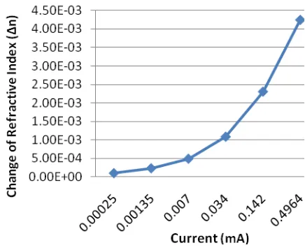
Figure 2.Change of refractive index at wavelength 1.55µm.
Figure 3. Change of refractive index at wavelength 1.3µ m.
Figure 2 and 3 show the relationship between drive current and the refractive index change at 1.55µm and 1.3µ m wavelength respectively. The refractive index change increase gradually when the drive current increase. The value of current to get phase shift is obtained from the graph by referring the equation (3). The results indicate that the current (I ) are 0.035mA for 1.55µm wavelength and 0.066mA for 1.3µm wavelength. This result shows an improvement with respect to [4]. The smaller current value of phase shift modulation at 1.55µ m wavelength shows that the modulator can perform batter when operate at the particular wavelength compared to 1.3µm wavelength.
Figure 4. Modulation Angle against drive current
Figure 4 shows the modulation angle against drive current for the modulator at two different wavelengths. Once again, the length of the device is assumed as 500 µm. We can see the different current is required to change the phase at a different angle. The change in modulation angle varies nonlinearly with applied current. Less drive current is required for a phase shift at a longer wavelength (1.55µm).
IV. CONCLUSION
The p-i-n diode structure has been chosen to simulate the characteristics of the modulator based on the refractive index change and the phase shift by using the effect of the current injection. Hopefully, this can be used as the guidance for the real experiment device. In conclusion, the phase modulator performance will depend on the value of the drive current (I ) in which have been used to get the phase shift. The smaller value of I is required to have the better phase modulator.
ACKNOWLEDGMENT
The authors would like to thank Universiti Teknikal Malaysia Melaka (UTeM) for the support and to the staffs of Photonic Technology Lab and Clean room of Institute of Microelectronic and Nanotechnology, Universiti Kebangsaan Malaysia for the guidance and co-operation.
REFERENCES
[1] G. T. Reed and A. P. Knights, Silicon Photonics –An Introduction, John Wiley & Sons (2004).
[2] R.A. Soref and J.P. Lorenzo, “All-silicon active and passive guided-wave components for = 1.3 and 1.6 µm,” IEEE Journal of Quantum Electronics, vol. QE-22, no.6, pp.873-879 (1986).
[3] P.D. Hewitt and G.T. Reed, “ Improving the response of optical phase modulator in SOI by computer simulation,” J. Lightwave Technol., vol.18, no.3, pp. 443-450, Mar 2000.
[4] Ching Eng Png, Seong Phun Chan, Soon Thor Lim and G.T Reed “ Optical Phase Modulators for MHz and GHz Modulation in Silicon – On-Insulator (SOI)” J. Lightwave Technol., vol.22, no.6, pp. 1573-1582, June 2004.
[5] R. A. Soref and B. R. Bennet, “Electrooptical effects in silicon”, Journal of Quantum Electronics, vol. QE-23, no. 1, pp. 123-129 (1987). [6] Z. Li, D. Xu, W.R. McKinnon, S. Janz, J.H. Schmid, P. Cheben and J. Yu, “Silicon waveguide modulator based on carrier depletion in periodically interleaved PN junctions”, Optics Express, vol. 17, no. 18, pp. 15947-15958 (2009).
[7] R.A Soref and B. R Bennett, “Kramers-Kronig analysis of electro-optical switching in silicon”, Proc. SPIE, vol.704, pp.1622-1631, 2004. [8] Zhi-Yong Li, Dan-Xia Xu, W. Ross Mc Kinnon, Siegfried Janz, Jens H.
Schmid, Pavel Cheben, and Jin-Zhong Yu, “Silicon waveguide modulator based on carrier depletion in periodically interleaved PN junctions”, Optics Express, Vol.17, No.18, pp. 15947-15958, 2009. [9] Giuseppe Coppola, Iodice Mario, Ivo Rendina, “Analysis of a planar
silicon optoelectronic modulator based on the waveguide- vanishing effect”, Proc. Of SPIE, Vol. 6593, 2007.
[10] L.Liao, D. Samara-Rubio, M.Morse, A. Liu, H. Hodge, D. Rubin, U.D Keil, T. Franck, “High Speed silic.on Mach- Zehnder modulator”, Opt. Express 13, pp.3129-3135, 2005.
[11] A. Brimont, F.Y Gardes, P. Sanchis, D. Marris-Morrini, P. Dumon, J.M Fedeli, L. O’Faolin, W. Boagert, L. Vivien, J. Marti, G.T Reed, and T.F. Krauss, “Design of a micro-ring resonator electro-optical modulator embedded in a reverse biased PN junction”, Proc. ECIO, ThD4, pp. 15947- 15958, 2008.
[12] Zhi-Yong Li, Dan-Xia Xu, W. Ross Mc Kinnon, Siegfried Janz, Jens H. Schmid, Pavel Cheben, and Jin-Zhong Yu, “Silicon waveguide modulator based on carrier depletion in periodically interleaved PN junctions”, Optics Express, Vol.17, No.18, pp. 15947-15958, 2009. [13] Giuseppe Coppola, Iodice Mario, Ivo Rendina, “Analysis of a planar
silicon optoelectronic modulator based on the waveguide- vanishing effect”, Proc. Of SPIE, Vol. 6593, 2007.
[14] V. R. Almeida, C. A. Barrios, R.R Panepucci, and M. Lipson, “All-optical control of light on a silicon chip”, Nature, vol.431, no.7012, pp. 1081-1084, 2004.
[15] Delphine Marris-Morrini, Xavier Le Roux, Daniel Pascal, Laurent Vivien, Eric Cassan, Jean Marc Fedeli, Jean Francois Damlencourt, David Bouville, Jose Palomo, and Suzanne Laval, “High speed all- silicon optical modulator”, Journal of Luminescence, vol. 121, pp.387-390, 2006.
[16] A.Cutolo, M.Iodice, A.Irace, P.Spirito, and Zeni, “An electrically controlled Bragg reflector integrated in a rib silicon on insulator waveguide,” Appl.Phys.Lett., vol.71, no.2, pp.199, 1997. [17] C. Angulos Barrios, V.R Almeida, and M. Lipson,
“Low-power-consumption short-length and high- modulation-depth silicon electro-optic modulator,” J. Lightwave Technol., vol.21, no.4, pp. 1089-1098, 2003.
[18] C. Angulos Barrios, V.R Almeida, R.Panepucci,and M. Lipson, “Electrooptic modulation of silicon-on-Insulator submicronmeter-size waveguide devices”, J. Lightwave Technol., vol.21, no.10, pp. 2332-2339, 2003..
[19] S. Libertino and A. Sciuto, Electro-Optical Modulators in Silicon, Springer Series in Optical Sciences (2006).