ICSE2010 Proc. 2010, Melaka, Malaysia
Operation mode of phase modulation based on carrier
dispersion effect in p-i-n diode of silicon rib
waveguide
Mardiana B, Hazura H, Hanim AR, Menon, P.S,
Member, IEEE
and Huda Abdullah,
Member, IEEE
Institute of Microengineering and Nanoelectronics (IMEN), Universiti Kebangsaan Malaysia (UKM)
43600 Bangi, Selangor, Malaysia Email: [email protected]
Abstract- This paper highlights the study of the carrier injection mode and the carrier depletion mode of the phase modulator. The phase modulator device has been integrated in the silicon rib waveguide by using the p-i-n diode structure. The electrical device performance is predicted by using the 2-D semiconductor package SILVACO (CAD) software under DC operation. Summarily, the phase modulator device has less sensitivity to the effective refractive index changes when operating in reverse biased or depletion mode compared to the forward biased or injection mode.
I. INTRODUCTION
Lately, silicon photonics have been intensively studied by many research groups with the intention of linking it between the field of optical communication and the silicon integrated circuits. The performance of the integrated circuit (IC) will be improved by the integrating of the optics and the electronics on a same chip; in which it could benefit the telecommunications for the development of low cost solutions for the high-speed optoelectronic devices and systems. There are many benefits of the silicon as a photonic medium [1][3]. Especially, it is transparent in the range of optical telecommunications wavelengths (1.3 and 1.55µm) and because of the high index of the refraction. Due to its uniqueness characteristic, silicon is very suitable material for the fabrication of the high-index-contrast sub-micrometer structures [1]. Furthermore, the matured silicon integrated circuit process technology in bipolar and complementary metal–oxide semiconductor provides the breakthrough of the implementation of dense silicon-based integrated optics and electronics on-chip.
It is well known the modulation achievement is very much dependable on the plasma dispersion effect and the thermal effects in the silicon. From the past research, it is proven that the most successful silicon optical modulators are based on the free carrier density. Its function is to control the optical effective refractive index device [1]. The speed and the efficiency of the free carrier density modulated in the waveguide will determine the performance of the free carrier plasma dispersion.
In this paper, the effective refractive index of the silicon is modulated electrically by injecting electrons and holes by using a p-i-n junction diode structure embedded in the rib waveguide.
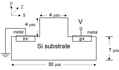
The modulator used the carrier depletion in a reversed biased and the carrier injection in a forward biased [2][3]. The active cross section of the phase modulator device has been used in this work is shown in fig. 1. The structure is different from ref. [1] in terms of the material used and the dimension chosen. In this study, we fabricate the waveguide on the pure silicon wafer.
Fig. 1, Active cross section of pin diode structure of phase modulator device.
The refractive index changes in silicon based on a free carrier concentration variation can be calculated from the equations derived by R.A Soref [8] from the Drude- Lorenz equations.
The equations are:
For o=1.55 :
n = - [8.8 x 10⁻²² Ne + 8.5 x 10 -18 ( Nh)0.8] (1)
For o=1.3 :
n = - [6.2 x 10⁻²² Ne + 6.0 x 10 -18 ( Nh)0.8] (2)
ICSE2010 Proc. 2010, Melaka, Malaysia
where n is the refractive index change and Ne and Nh are the electron and hole concentration variations, respectively.
II. DEVICE DESIGN
There are two parts in the development of the simulation. The first part is the simulation of the device fabrication and the second part is the simulation of the device analysis. In the first part, the simulation development has been developed by using the component of the 2D package Silvaco software, the ATHENA.
The design of the simulation is begin by the construction of the p-i-n diode structure. The P+ type region is doped with 5x1018 cm-3 boron concentrations while the N+ type region is doped with 5x1018cm-3 phosphorus concentrations. The structure had a background doping concentrations of 1x 10¹⁴. The depth of the doped region is about 1.8 m for N+ region and 1.6 m for P+ region. The rib height and width for the structure is chosen in order to have a single mode behaviour. The rib structure is designed to have 4 µ m in height and 4 µ m in width.
Other component of the SILVACO device simulation package; the ATLAS, have been used in this work to simulate the device operation. The refractive index was change by injecting the free carriers in the optical guiding region. The simulator has been used to determine the change of refractive index with the optical wavelength 1.3µ m and 1.55µm.
The Silvaco ATLAS will simulates the internal physics and device characteristics by using the Poisson’s equation and the charge continuity equations for the electrons and holes calculation. The software also uses a complete statistical approach (Fermi–Dirac statistics). The Carrier recombination models are also included with the Shockley–Read–Hall (SRH) recombination, Auger recombination, and the surface recombination.
TABLE I SIMULATIONS PARAMETER
Si refractive index 3.475
Si background carrier conc. (cm-3) 1x10¹⁴
p 2x10⁻⁶
n 2x10⁻⁶
Temperature (K) 300
III. RESULT AND DISCUSSION
In this study, the active region of the modulator have been tested under DC operation. The active device will be operated by applying an external electrical signal to the electrodes. The disturbed free carriers will cause a distinct change in the effective refractive index [5].
Two type of dc testing have been done in this work. They are forward biased and the reverse biased. In the forward biased, a
positive bias is applied to the P electrode. It is expected, the extra carriers will be injected into the waveguide.
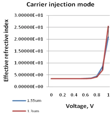
Fig. 2, Effective refractive index change for increasing forward bias voltage.
Fig. 2 shows the result of the effective refractive index changes by varies the forward bias voltage from 0 to 1V. The result show the effective refractive index have changed drastically at 0.9V onwards. The index variation of 1.74x10 is obtained in between 0V and 1V.It’s means, the effective refractive index have a high sensitivity changes with a little increasing of forward bias value after 0.9V and it will give a significant effect to the phase modulation. By injecting both holes and electrons in the active region of the modulator, a much higher changes in the index of the refraction can be realized. It is due to both electrons and holes contribution.
Fig.3, Effective refractive index change for increasing reverse bias voltage.
ICSE2010 Proc. 2010, Melaka, Malaysia
In the reverse biased testing, a negative bias is applied to the P electrode in which it will change the width of the depletion region thus eventually changing the effective refractive index. Fig. 3 shows the changes of effective refractive index in reverse bias. The effective index variation increases as the reverse bias voltage increases. The index variation of 5.09x10⁻⁴ is obtained between 0V and -8V.Its indicate the index variation value of the effective refractive index in reverse bias is much more smaller than the value of the index variation in the forward bias testing.
When a reverse bias is applied to the diode, the holes were rid out. The holes concentration variation is responsible for the effective index variation in which created a phase shift of the guided mode. To get a high effective refractive index changes, a huge overlapping between the carrier density zone and the guided mode must be obtained.
IV. CONCLUSION
In conclusion, the p-i-n diode structure of phase modulator device had much greater sensitivity to the effective refractive index changes when operating under forward bias after 0.9V onwards compared to the reverse bias or the depletion mode.
ACKNOWLEDGMENT
The authors would like to thank Universiti Teknikal Malaysia Melaka (UTeM) for the support and to the staffs of Photonic Technology Lab and Clean room of Institute of Microelectronic and Nanotechnology, Universiti Kebangsaan Malaysia for the guidance and co-operation.
REFERENCES
[1] S. J. Spector, M. W. Geis, M. E. Grein, R. T. Chulein, J. U. Yoon, D. M. Lennon, F. Gan, G.-R. Zhou, F. X. Kaertner2, and T. M. Lyszczarz1, “High-speed silicon electro-optical modulator that can be operated in carrier depletion or carrier injection mode*”, Optical Society of America (2008) .
[2] A Liu, L. Liao, D. Rubin, H. Nguyen, B. Ciftcioglu, Y. Chetrit, N. Izhaky, and M. Paniccia, “High-speed optical modulation based on carrier depletion in a silicon waveguide," Opt. Express 15, 660-668 (2007). [3] Q. Xu, S. Manipatruni, B. Schmidt, J. Shakya, and M. Lipson “12.5 Gbit/s
carrier-injection-based silicon micro-ring silicon modulators ,"Opt. Express 15, 430-436 (2007).
[4] L.Liao, D. Samara-Rubio, M.Morse, A. Liu, H. Hodge, D. Rubin, U.D Keil, T. Franck, “High Speed silic.on Mach- Zehnder modulator”, Opt. Express 13, pp.3129-3135, (2005).
[5] A. Brimont, F.Y Gardes, P. Sanchis, D. Marris-Morrini, P. Dumon, J.M Fedeli, L. O’Faolin, W. Boagert, L. Vivien, J. Marti, G.T Reed, and T.F. Krauss, “Design of a micro-ring resonator electro-optical modulator embedded in a reverse biased PN junction”, Proc. ECIO, ThD4, pp. 15947- 15958, (2008).
[6] Zhi-Yong Li, Dan-Xia Xu, W. Ross Mc Kinnon, Siegfried Janz, Jens H. Schmid, Pavel Cheben, and Jin-Zhong Yu, “Silicon waveguide modulator based on carrier depletion in periodically interleaved PN junctions”,
Optics Express, Vol.17, No.18, pp. 15947-15958,( 2009).
[7] Giuseppe Coppola, Iodice Mario, Ivo Rendina, “Analysis of a planar silicon optoelectronic modulator based on the waveguide- vanishing effect”, Proc. Of SPIE, Vol. 6593, (2007).
[8] R.A Soref and B. R Bennett, “Kramers-Kronig analysis of electro-optical switching in silicon”, Proc. SPIE, vol.704, pp.1622-1631, (2004). [9] Delphine Marris-Morrini, Xavier Le Roux, Daniel Pascal, Laurent
Vivien, Eric Cassan, Jean Marc Fedeli, Jean Francois Damlencourt, David Bouville, Jose Palomo, and Suzanne Laval, “High speed all- silicon optical modulator”, Journal of Luminescence, vol. 121, pp.387-390, (2006).
[10] C. Angulos Barrios, V.R Almeida, R.Panepucci,and M. Lipson, “Electrooptic modulation of silicon-on-Insulator submicronmeter-size waveguide devices”, J. Lightwave Technol., vol.21, no.10, pp. 2332-2339, (2003).