Abstract — This paper reports the effect of doping concentration to the electrical characteristic performance of the phase modulator in the carrier injection mode at wavelength 1.55µm. The phase modulator device has been integrated in the silicon-on-insulator (SOI) rib waveguide with the p-i-n diode structure. The electrical device performance is predicted using the 2-D semiconductor package SILVACO (CAD) software under DC operation. The least doping concentration of p+ and n+ region produces the least change of refractive index of the modulator. Meanwhile, results show that by increasing the doping concentrations, the value of I decreases. This means that the phase modulator performance is better with increased doping concentrations.
Index Terms—Phase modulator, Silicon-on-Insulator, carrier injection, refractive index change.
I. INTRODUCTION
ECENTLY, silicon-on-insulator (SOI) has been widely used as a photonic substrate in many research studies due to its unique characteristic [1]. Furthermore, the matured process of silicon in microelectronic fabrication process is the reason why SOI are the most chosen for many photonic devices such as the modulator [1,2]. The phase modulator is one of the basic components for the more complex photonic integrated circuits. It is developed based on free carrier plasma dispersion effect in the waveguide. The phase shift can be obtained by inducing more free carrier in the optical guiding region with the purpose to change the refractive index value
Manuscript received March 26, 2010. Mardiana B. is with Universiti Teknikal Malaysia Melaka, Locked Bag No.1752, Durian Tunggal Post Office, 76109, Durian Tunggal, Malacca, Malaysia (phone: +60173674795;fax:+6038925809;e-mail:[email protected]).She is currently working towards the PhD degree under the supervision of Prof Shahbudin Saari at the IMEN, Unniversiti Kebangsaan Malaysia.
Hazura H. is with Universiti Teknikal Malaysia Melaka, Locked Bag No.1752, Durian Tunggal Post Office, 76109, Durian Tunggal, Malacca, Malaysia (phone: +601336531205 ;fax:+6038925809;e-mail:[email protected]). She is currently working towards the PhD degree under the supervision of Prof Shahbudin Saari at the same university
Hanim A.R. is with Universiti Teknikal Malaysia Melaka, Locked Bag No.1752, Durian Tunggal Post Office, 76109, Durian Tunggal, Malacca, Malaysia (phone: +60133989002 ;fax:+6038925809;e-mail:[email protected]). She is currently working towards the PhD degree under the supervision of Prof Shahbudin Saari at the same university.
Sahbudin Saari. is with Institute of Microengineering and nanoelectronics, 43600 Bangi, Selangor (phone: +60389216308; fax:+6038925809;e-mail:[email protected]). In 2003, he joined IMEN as Professor and also Principal Fellow works on Photonic Technologies Research and Development.
[3]. Although there are many studies on the design of the phase modulator had been done before, the most challenging tasks is to design the more efficient, high speed and low loss phase modulator. In this paper, we propose a design of p-i-n diode structure phase modulator with a specific dimension based on rib waveguide formed from SOI materials and operating at important optical communications wavelengths of 1.55 µm [3, 4]. Soref and Bennet [7] quantified the changes they had identified from the research for the refractive index and in the absorption coefficients. The following equations are widely used in order to evaluate changes due to injection or depletion of carriers in silicon and hence are utilized in this report:
At 0 = 1.55 m:
n = ne + nh = -[8.8 x 10⁻²² Ne + 8.5 x 10 -18 ( Nh)0.8] (1) At 0 = 1.3 m:
n = ne + nh = -[6.2 x 10 -22
Ne + 6.0 x 10 -18
( Nh)0.8] (2) where:
ne change in refractive index resulting from change in free electron carrier concentrations.
nh change in refractive index resulting from change in free hole concentrations.
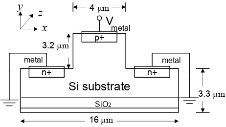
The active cross section of the phase modulator device has been used in this work is shown in Figure 1.
Figure 1: Cross section of the p-i-n phase modulator.
Various Doping Concentration Effect on
Silicon-on-Insulator (SOI) Phase Modulator
Mardiana B, Hazura H, Hanim A.R, Sahbudin Shaari,
Member, IEEE,
Huda Abdullah
R
ICP2010-101
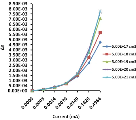
By observing the doping concentrations variations at the waveguide centre (x=4 m, y=8 m), it enable us to work out for the refractive index change for a specific forward bias voltage and therefore the resulting phase shift of the device, in which the relationship can be summarized as:
= 2 nL/ (3) where L is the length of the modulator. In this work, the length of the modulator is assumed as 500µm.
II. PHASE MODULATOR DESIGN
The simulation process is divided into two parts. The first part is the simulation of the device fabrication and the second part is the simulation of the device analysis. In the first part, the simulation development has been developed using the component of the 2D package SILVACO software, the ATHENA.
The design of the simulation begins by the construction of the p-i-n diode structure. The P+ type region is doped with 5x1018 cm3 boron concentrations while the N+ type region is doped with 5x1018cm3 phosphorus concentrations. The structure has a background doping concentrations of 1x 1014 cm3. The depth of the doped region is about 1.8 m for N+ region and 1.6 m for P+ region. The rib height and width for the structure is chosen to have a single mode behaviour. The rib structure is designed to have 3.2 µ m in height and 4 µ m in width.
ATLAS, another component of the SILVACO device simulation package has been utilized to simulate the device operation. The software simulates the internal physics and device characteristics using the Poisson’s equation and the charge continuity equations for the electrons and holes calculation. The software also uses a complete statistical approach (Fermi–Dirac statistics). The Carrier recombination models are also included with the Shockley–Read–Hall (SRH) recombination, Auger recombination, and the surface recombination.
The simulator has been used to determine the change of refractive index at the optical wavelength 1.55µm. The important parameters used in the simulations are shown in Table 1.
TABLE 1
SIMULATION PARAMETERS
Si refractive index 3.475
Si background carrier conc. (cm3) 1x10¹⁴
p (sec) 2x10
-6
n (sec) 2x10⁻⁶
Temperature (K) 300
III. RESULTS AND DISCUSSION
The DC characteristic is done by employing a forward-biased effect with 0.75, 0.8, 0.85, 0.9, 0.95 and 1V. The results are depicted in Figure 2 and Table 2.
Figure 2: Refractive index change against various doping concentration of p+ and n+ regions.
Figure 2 displays the change of refractive index with different doping concentrations of p+ and n+ regions. The least doping concentration of p+ and n+ region produces the least change of refractive index of the modulator. For instance, with 0.4964 mA drive current, the refractive index change for concentration of 5E17cm3 is 4.76021E-03. Meanwhile, at doping concentration of 5E21cm3 with the same drive current, the change of refractive index is larger with 7.781809E-03. Therefore, higher doping concentration is in favour for a larger refractive index change.
TABLE 2
Doping Concentration (cm3) I (mA) 5e17
5e18 5e19 5e20 5e21
0.0448 0.0313 0.0286 0.0259 0.0245
One of the method to evaluate the performance of a modulator is by determining the current (I ) needed for a 180° of phase shift. Lower value of I is favorable since lower drive current is needed for a modulator to modulate the phase. By using (3), the value of refractive index change for 180° phase shift of the design is 1.5E-3. Therefore, the value of I is obtained from graph in Figure 2. The values of I against various doping concentrations are depicted in Table 2. Table 2 concludes that by increasing the doping concentrations, the value of I decreases. This means that the phase modulator performance is better with increasing doping concentrations.
IV. CONCLUSION
Further optimization of experimental devices based on the predicted results and scope are promising. While this paper discusses the results of a specific phase modulator design, the results suggest that increasing the doping concentrations of p+ and n+ regions would also enhance the performance of other p-i-n phase modulator geometries, although there would clearly need to be a specific evaluation of any design.
ACKNOWLEDGMENT
The authors would like to thank Universiti Teknikal Malaysia Melaka (UTeM) for the support and to the staffs of Photonic Technology Lab and Clean room of Institute of Microelectronic and Nanotechnology, Universiti Kebangsaan Malaysia for the guidance and co-operation.
REFERENCES
[1] G. T. Reed and A. P. Knights, Silicon Photonics –An Introduction, John Wiley & Sons (2004).
[2] R.A. Soref and J.P. Lorenzo, “All-silicon active and passive guided-wave components for = 1.3 and 1.6 µm,” IEEE Journal of Quantum Electronics, vol. QE-22, no.6, pp.873-879 (1986).
[3] P.D. Hewitt and G.T. Reed, “ Improving the response of optical phase modulator in SOI by computer simulation,” J. Lightwave Technol., vol.18, no.3, pp. 443-450, Mar 2000.
[4] Ching Eng Png, Seong Phun Chan, Soon Thor Lim and G.T Reed “ Optical Phase Modulators for MHz and GHz Modulation in Silicon – On-Insulator (SOI)” J. Lightwave Technol., vol.22, no.6, pp. 1573-1582, June 2004.
[5] R. A. Soref and B. R. Bennet, “Electrooptical effects in silicon”,
Journal of Quantum Electronics, vol. QE-23, no. 1, pp. 123-129 (1987). [6] Z. Li, D. Xu, W.R. McKinnon, S. Janz, J.H. Schmid, P. Cheben and J. Yu, “Silicon waveguide modulator based on carrier depletion in periodically interleaved PN junctions”, Optics Express, vol. 17, no. 18, pp. 15947-15958 (2009).
[7] R.A Soref and B. R Bennett, “Kramers-Kronig analysis of electro-optical switching in silicon”, Proc. SPIE, vol.704, pp.1622-1631, 2004. [8] Zhi-Yong Li, Dan-Xia Xu, W. Ross Mc Kinnon, Siegfried Janz, Jens H.
Schmid, Pavel Cheben, and Jin-Zhong Yu, “Silicon waveguide modulator based on carrier depletion in periodically interleaved PN junctions”, Optics Express, Vol.17, No.18, pp. 15947-15958, 2009. [9] Giuseppe Coppola, Iodice Mario, Ivo Rendina, “Analysis of a planar
silicon optoelectronic modulator based on the waveguide- vanishing effect”, Proc. Of SPIE, Vol. 6593, 2007.
[10] L.Liao, D. Samara-Rubio, M.Morse, A. Liu, H. Hodge, D. Rubin, U.D Keil, T. Franck, “High Speed silic.on Mach- Zehnder modulator”, Opt. Express 13, pp.3129-3135, 2005.
[11] A. Brimont, F.Y Gardes, P. Sanchis, D. Marris-Morrini, P. Dumon, J.M Fedeli, L. O’Faolin, W. Boagert, L. Vivien, J. Marti, G.T Reed, and T.F. Krauss, “Design of a micro-ring resonator electro-optical modulator embedded in a reverse biased PN junction”, Proc. ECIO, ThD4, pp. 15947- 15958, 2008.
[12] Zhi-Yong Li, Dan-Xia Xu, W. Ross Mc Kinnon, Siegfried Janz, Jens H. Schmid, Pavel Cheben, and Jin-Zhong Yu, “Silicon waveguide modulator based on carrier depletion in periodically interleaved PN junctions”, Optics Express, Vol.17, No.18, pp. 15947-15958, 2009. [13] Giuseppe Coppola, Iodice Mario, Ivo Rendina, “Analysis of a planar
silicon optoelectronic modulator based on the waveguide- vanishing effect”, Proc. Of SPIE, Vol. 6593, 2007.
[14] V. R. Almeida, C. A. Barrios, R.R Panepucci, and M. Lipson, “All-optical control of light on a silicon chip”, Nature, vol.431, no.7012, pp. 1081-1084, 2004.
[15] Delphine Marris-Morrini, Xavier Le Roux, Daniel Pascal, Laurent Vivien, Eric Cassan, Jean Marc Fedeli, Jean Francois Damlencourt, David Bouville, Jose Palomo, and Suzanne Laval, “High speed all- silicon optical modulator”, Journal of Luminescence, vol. 121, pp.387-390, 2006.
[16] A.Cutolo, M.Iodice, A.Irace, P.Spirito, and Zeni, “An electrically controlled Bragg reflector integrated in a rib silicon on insulator waveguide,” Appl.Phys.Lett., vol.71, no.2, pp.199, 1997. [17] C. Angulos Barrios, V.R Almeida, and M. Lipson,
“Low-power-consumption short-length and high- modulation-depth silicon electro-optic modulator,” J. Lightwave Technol., vol.21, no.4, pp. 1089-1098, 2003.
[18] C. Angulos Barrios, V.R Almeida, R.Panepucci,and M. Lipson, “Electrooptic modulation of silicon-on-Insulator submicronmeter-size waveguide devices”, J. Lightwave Technol., vol.21, no.10, pp. 2332-2339, 2003..
[19] S. Libertino and A. Sciuto, Electro-Optical Modulators in Silicon, Springer Series in Optical Sciences (2006).