Vol. 21, No. 1 (2012) 1250004 (8pages) c
World Scientific Publishing Company DOI:10.1142/S021886351250004X
DESIGN AND CHARACTERIZATION OF MULTIPLE COUPLED MICRORING BASED WAVELENGTH DEMULTIPLEXER IN SILICON–ON–INSULATOR (SOI)
HAZURA HAROON∗, SAHBUDIN SHAARI, P. S. MENON, B. MARDIANA, A. R. HANIM, N. ARSAD, B. Y. MAJLIS,
W. M. MUKHTAR and HUDA ABDULLAH Institute of Microengineering and Nanoelectronics (IMEN),
Universiti Kebangsaan Malaysia (UKM), 43600 UKM Bangi, Selangor, Malaysia
Received 15 November 2011 Published 23 April 2012
We report in this paper, an optimized design and characterization of SOI based single mode, four channels wavelength demultiplexer using microrings. The usage of silicon-on-insulator (SOI) allows a wide free spectral range (FSR) for the device that is crucial in developing ultra-compact integrations of planar lightwave circuits (PLCs). The char-acterizations are done using Finite-Difference Time-Domain (FDTD) mode simulations from RSOFT. Serially cascaded microring arrays up to the third order are presented to study the design trade-off among the FSR, Q-factor and optical losses of the later-ally coupled wavelength demultiplexer. The demultiplexer is expected to be working at C-band region of Wavelength Division Multilplexing (WDM) for a wavelength around 1550 nm. Our proposed demultiplexer has low insertion loss (<0.5 dB) and a crosstalk around 12∼19 dB.
Keywords: Microring resonator; silicon photonic; silicon-on-insulator; wavelength demultiplexer.
1. Introduction
Selecting or combining the desired wavelengths in wavelength division tiplexing (WDM) system can be done with the application of wavelength mul-tiplexer/demultiplexer. The basic structure of the MRRs based wavelength multi/demultiplexer consists of two input/output waveguides and a ring. Previous researchers have been working on various types of materials for device fabrication such as silica, silica-on-silicon, polymers, lithium niobate and so forth.5,6 Even so, in our work, emphasis is put on silicon-on-insulator (SOI) owing to its numerous advantages such as high-index contrast, low-cost and its compatibility with the available fabrication facility.7−9
In this paper, Finite-Difference Time-Domain (FDTD) numerical simulations are utilized to analyze the design and characterization of 1×4 SOI-based wavelength
demultiplexer. The tools not only ease the design process but reduce the working time and cost as well. First, key design parameters such as waveguide size and gap width between waveguides are optimized. Then the device performance in terms of FSR, Q-factor, as well as insertion loss and crosstalk are investigated.
2. Device Description and Theory
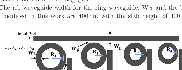
Figure 1 shows the schematic diagram of the proposed configuration of the first order wavelength demultiplexer. The demultiplexer consists of a straight input bus waveguide, four output waveguides and four laterally cascaded microring uides. The light input is coupled into the bus waveguide and the microring waveg-uides that serve as resonant optical cavities. Four wavelengths: λ1, λ2, λ3 and λ4 from input port are separated into four distinctive output channels according to wavelength in resonance with the corresponding ring waveguides which have four different ring radii. Unequal ring radius will resonate with signals of different carrier wavelengths. Hence, the four input wavelengths can be extracted into four different output channels, functioning as drop demultiplexer. The bending loss of the output channels is assumed to be negligible.
The rib waveguide width for the ring waveguide, WR and the bus waveguide, WB modeled in this work are 400 nm with the slab height of 400 nm, fabricated
Wg WB
Input Port
Through Port
λ4 λ3
λ2 λ1
Drop Port1 Drop Port2 Drop Port3 Drop Port4 λ1 , λ2 , λ3 , λ4
R1 R2
R3 R4
WR
Wg
on top of 700 nm buried oxide layer. The gap distances between the input/output waveguides and the ring waveguide (Wg) are 300 nm, same as the gap size between serially cascaded ring waveguides. We assume that all the silicon waveguides have the same refractive index of 3.5 while the refractive indexes for SiO2 and air are 1.45 and 1.0, respectively.
The power emitted at the through port and the drop port for single microring can be estimated according to the formula10:
Tthrough=
(λ−λ0)2+F SR4π
2
(κ2p)2
(λ−λ0)2+F SR4π
2
(2κ2+κ2 p)2
(2.1)
Tdrop=
4xF SR
4π
2
(κ4)
(λ−λ0)2+F SR4π
2
(2κ2+κ2 p)2
(2.2)
whereλ0is the resonant wavelength,κ2is the power coupling coefficient between the bus waveguide and the resonator, andκ2
p is the propagation power loss coefficient per round trip in the microring resonator.
The important characteristics of the MRRs based wavelength demultiplexer are the Free Spectral Range (FSR), Quality Factor (Q-factor), insertion loss and crosstalk. A wide FSR is demanded in Wavelength Division Multiplexing (WDM) system. Larger FSR means more signal can be accommodated into a channel at the same time. Its value is determined by11:
F SR≈ λ
2 0
ng(λ)Leff
(2.3)
whereng is the group index andLeff is the effective length of the device.
The Q-factor as a measure of wavelength selectivity, can be defined as the ratio of the power stored to the power dissipated in the ring.12It portrays the sharpness of resonant peak, and it can be calculated according to the following formula.
Q≈ λ0
(∆λ)3dB
= 2πngrLeff 2λ0arccos[1+|
t|2τ2−4|t|τ
−2|t|τ ]
(2.4)
Here, ngr is the group velocity,Leff the effective length,τ is field attenuation and
ttransmission coefficient.
The microring efficiency can be determined by crosstalk; the difference between the output power at the through port and the drop port, while insertion loss can be measured by comparing the output power of the device to a reference input power.13 Insertion loss is one of the most important specifications in determining the maximum power loss.14
3. Results and Discussions
characteristics obtained by 2D numerical simulations. Then, the performance of the optimized design will be discussed in details in terms of the crosstalk and the insertion loss.
3.1. Design optimization
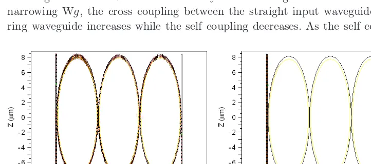
We have selected the values 6µm, 8µm, 10µm and 12µm forR1, R2,R3 andR4 respectively, of the ring radii for the proposed device. A large increment in ring radii is due to the fact that a very small difference in ring radii is hard to fabricate. The resonance behavior can be explained by Fig. 2 where it shows the on-resonance and off-resonance state for the third order microring resonators with R = 6µm, Wg= 30 nm, WB = 400 nm and WR = 400 nm. In general, resonances in a ring are expected to occur atλ0and its multiples if the resonant condition as given below15 is satisfied,
neffL=mλ0 (3.1)
where neff is the effective index of the circular waveguide, L is the length of the ring, and m is an integer. In this condition, the input signal with wavelength λ0 will be coupled into the ring waveguide and all others will be transmitted to the through port [Fig. 2(a)]. At off-resonance state, input signal will bypass the ring and emitted at the through port [Fig. 2(b)]. L is 2πR, therefore it can be clearly seen that the resonance condition is dependable on the ring radii.
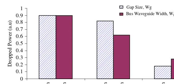
Three different gap sizes, Wg have been studied and the output power of the single microring device with R = 8µm, WR = 400 nm,WB = 400 nm are plotted in Fig. 3. It is seen that the best result is obtained for gap size of 30 nm. The coupling strength reduced by 80% when the distance between the channel waveguide and ring or distance between two serially cascaded rings increased to 100 nm. By narrowing Wg, the cross coupling between the straight input waveguide and the ring waveguide increases while the self coupling decreases. As the self coupling is
(a) (b)
0 0.1 0.2 0.3 0.4 0.5 0.6 0.7 0.8 0.9
1 Gap Size, Wg
Bus Waveguide Width, WB
30nm 400nm 50nm 500nm 100nm 600nm
[image:5.595.90.370.61.197.2]Dropped Power (a.u)
Fig. 3. Spectral responses of MRRs based device with various gap sizes and waveguide channel widths.
reduced, more power is coupled to the drop port whereas the nonresonant output power at the through port is reduced. Figure 3 also shows the effect of varying the bus waveguide width, WB on the device performance (with R = 8µm, Wg= 30 nm and WR = 400 nm). It is obvious that the output power dropped as the channel waveguide width is increased. Channel waveguide width of 600 nm produced the lowest output transmission where less than 50% of the input signal is coupled to the output waveguide. Yet, thin waveguides are hard to fabricate by conventional lithography and E-beam lithography is required.
Figure 4 presents the plots of the transmission response of the device with single ring and those of doubly and triply cascaded microring with R = 8µm, Wg= 30 nm, WR = 400 nm and WB = 400 nm. It can be observed that regardless the number of seriated rings, FSR remains 12 nm but the output power was decreased. It is worthwhile to understand that higher seriated microrings will suffer more attenuation due to longer transmission length. To enhance the device performance,
0 0.1 0.2 0.3 0.4 0.5 0.6 0.7 0.8 0.9 1
1540 1545 1550 1555 1560
1st 2nd 3rd
Wavelength, nm
[image:5.595.123.338.454.585.2]Dropped Power (a.u)
6µm 8µm 10µm 12µm
0 0.1 0.2 0.3 0.4 0.5 0.6 0.7 0.8 0.9 1
1540 1545 1550 1555 1560
Wavelength, nm
[image:6.595.112.350.63.194.2]Dropped Power (a.u)
Fig. 5. Spectral responses of the MRRs device with various radii.
new device designs are expected; hence, intensive studies in the device modeling are demanded in the future research.
In Fig. 5, we observed the effect of varying ring radii on MRR. The MRR resonated at different wavelengths, giving different FSR values. Here, we use the optimized value of waveguide channel width and gap width (WB = 400 nm and Wg= 30 nm). It is interesting to notice that, the FSR was proportional to the ring radii. This result agrees well with theoretical calculations predicting that shrinking the ring radii will increase the FSR.16In addition, the Q-value is raised as the ring radii are reduced. For instance, the Q-value calculated from the graph is 486 for 8µm and 321 for 12µm.
3.2. Demultiplexer performance
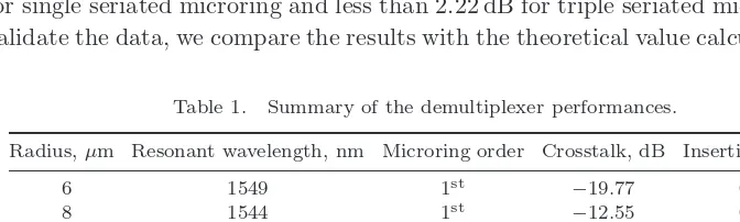
From Fig. 5, it is clearly seen that, the design is suitable for multiplexing device working at 1549 nm, 1544 nm, 1541 nm and 1554 nm wavelength. Non-uniform wave-length spacing occur due to huge ring radii different. Table 1 summarizes the perfor-mance of the proposed device. The insertion loss of all channels is less than 0.5 dB for single seriated microring and less than 2.22 dB for triple seriated microrings. To validate the data, we compare the results with the theoretical value calculated using
Table 1. Summary of the demultiplexer performances.
Radius,µm Resonant wavelength, nm Microring order Crosstalk, dB Insertion loss, dB
6 1549 1st
−19.77 0.222
8 1544 1st
−12.55 0.457
10 1541 1st −
16.53 0.457
12 1554 1st −
19.54 0.457
6 1549 3rd −
13.80 0.177
8 1544 3rd
−10.79 2.212
10 1541 3rd
−10.00 2.212
12 1554 3rd
[image:6.595.63.399.511.612.2]formula of transfer functions.16Our design has a better insertion loss, thereby prov-ing that a low loss can be obtained in the proposed device. The crosstalk is about 12–20 dB for single microring and becomes higher for the third order microrings for all ring radii.
4. Conclusion
We proposed a demultiplexer design composed of microring resonator with four output channels, investigated by FDTD software. The designed device has a good performance with low insertion loss, and low crosstalk. To improve the performance of the proposed device, further optimization of design parameters such as ring radii, microring orders, and ring width must be considered. This work will be continued with fabrication of the device and its characterization. For this purpose, the present analyses will provide useful guidance before laboratory works are carried out.
Acknowledgments
The authors would like to thank Universiti Teknikal Malaysia Melaka (UTeM) for the support and to the staff of Photonic Technology Lab, Institute of Micro-electronic and Nanotechnology (IMEN), Universiti Kebangsaan Malaysia for assis-tance and guidance. The Ministry of Higher Education of Malaysia and Universiti Kebangsaan Malaysia (UKM) is gratefully acknowledged for the grant under indus-trial Project -2011-015 and UKM-OUP- NBT-27-119/2011.
References
1. M. H. K. S. Xiao, H. Shen and M. Qi, A highly compact third-order silicon microring add-drop filter with a very large free spectral range, a flat passband and a low delay dispersion,Optics Express15(22) (2007) 14765–14771.
2. F. Xia, L. Sekaric and Y. Vlasov, Ultracompact optical buffers on a silicon chip,
Nature Photonics1(2007) 65–71.
3. C. Y. Chao, W. Fung and L. J Guo, Polymer microring resonators for biochemical sensing applications,Optics Express18(2) (2010) 393–400.
4. B. E. Little, S. T. Chu, H. A Haus, J. Foresi and J.-P. Laine, Miroring resonator channel dropping filters,IEEE J. of Lightwave Technology15(6) (1997) 998–1005.
5. P. Rabiei, W. H Steier, Z. Cheng and L. R Dalton, Polymer micro-ring filters and modulators,J. of Lightwave Tech.20(2002) 1968–1975.
6. S. J. Choi, K. Dordjev, S. J. Choi, P. D. Dapkus, W. Lin, G. Griffel, R. Menna and J. Connolly, Microring resonators vertically coupled to buried heterostructure bus waveguides,IEEE Photonics Technology Letters20(3) (2004) 828–830.
7. H. Hazura, A. R. Hanim, B. Mardiana and P. S. Menon, An analysis of silicon waveg-uide phase modulation efficiency based on carrier depletion effect, in IEEE
Inter-national Conference on Semiconductor Electronics 2010 (ICSE ’10), Malaysia (June
2010), pp. 348–350.
8. S. Shaari, A. R. Hanim, B. Mardiana, H. Hazura and P. S. Menon, Modeling and anal-ysis of lateral doping region translation variation on optical modulator performance,
inthe 4th Asian Physics Symposium AIP Conference Proceedings 1325(September
9. H. Hazura, A. R. Hanim, B. Mardiana, S. Shaari and P. S. Menon, Free carrier absorption loss of p-i-n silicon-on-insulator (SOI) phase modulator, inInternational
Conference on Enabling Science and Nanotechnology (Escinano) 2010 Proceedings,
Malaysia (Disember, 2010).
10. S. Xioa, M. H. Khan, H. Shen and M. Qi, Modeling and measurement of losses in silicon-on-insulator resonators and bends,Optics Express15(17) (2007) 10553–10561.
11. http://www.apollophoton.com/apollo/APNT/APN-APSS-RingResonator.pdf. 12. A. Vorckel, M. Monster, W. Henschel, P. H. Bolivar and H. Kurz, Asymetrical coupled
silicon-on-insulator microring resonators for compact add-drop multiplexers,Photon. Technol. Letter15(2003) 921–923.
13. J. Colachino, Mux/Demux optical specifications and measurement, Lightchip Inc (2001).
14. O. Schwelb, Crosstalk and bandwidth of lossy microring add/drop multiplexers,Optics
Communications265(2006) 175–179.
15. C.-Y. Chao and L. J. Guo, Design and optimization of microring resonators in bio-chemical sensing applications,J. Lightwave Technol.24(3) (March 2006), pp. 1395–
1402.
16. W. Y. Deng, D. G. Sun, S. L. E. and W. Xu, Analysis of a 1×32 polymer microring
resonant wavelength de-multi/multiplexer assistant with interleave filter,Optik120