Abstract— In this study, the Taguchi method was used to optimize the effect of HALO structure or halo implant variations on threshold voltage (VTH) and leakage current (ILeak) in 45nm p-type
Metal Oxide Semiconductor Field Effect Transistors (MOSFETs) device. Besides halo implant dose, the other process parameters which used were Source/Drain (S/D) implant dose, oxide growth temperature and silicide anneal temperature. This work was done using TCAD simulator, consisting of a process simulator, ATHENA and device simulator, ATLAS. These two simulators were combined with Taguchi method to aid in design and optimize the process parameters. In this research, the most effective process parameters with respect to VTH and ILeak are halo implant dose (40%) and S/D
implant dose (52%) respectively. Whereas the second ranking factor affecting VTH and ILeak are oxide growth temperature (32%) and halo
implant dose (34%) respectively. The results show that after optimizations approaches is -0.157V at ILeak=0.195mA/µm.
Keywords—Optimization; p-type MOSFETs device; HALO Structure; Taguchi Method.
I. INTRODUCTION
HE Metal-Oxide Semiconductor Field Effect Transistor (MOSFET) has been a popular device as it usually used in digital circuits, microprocessor, memory circuit, and other logic application of many kinds. In order to improve electrical device performance in circuit, MOSFETs have been scaled down successfully over the past few decades [1]. The MOSFET includes a channel of n-type or p-type
F.Salehuddin is with the College of Graduate Studies (COGS), Universiti Tenaga Nasional, Campus Putrajaya, 43009 Kajang, Selangor Malaysia (e-mail: [email protected]).
I.Ahmad was with the Institute of Microengineering and Nanoelectronic (IMEN), University of National Malaysia, Bangi. He is now with the Department of Electronics and Communication Engineering, College of Engineering (COE), Universiti Tenaga Nasional, Campus Putrajaya, 43009 Kajang, Selangor Malaysia (e-mail: [email protected]).
F.A.Hamid is with the Department of Electronics and Communication Engineering, College of Engineering (COE), Universiti Tenaga Nasional, Campus Putrajaya, 43009 Kajang, Malaysia (e-mail: [email protected]).
A.Zaharim is with the Faculty of Engineering and Built Environment, Universiti Kebangsaan Malaysia, 43600 Bangi, Selangor Malaysia (e-mail: [email protected]).
H.A.Elgomati is with the IMEN, Universiti Kebangsaan Malaysia, 43600 Bangi, Selangor Malaysia (e-mail: [email protected]).
B.Y.Majlis is with the Institute of Microengineering and Nanoelectronic (IMEN), Universiti Kebangsaan Malaysia, 43600 Bangi, Selangor Malaysia (e-mail: [email protected]).
P.R.Apte is with the Department of Electrical Engineering, Indian Institute of Technology (IIT), Bombay, Powai 400076 Mumbai, India (e-mail:
semiconductor material is accordingly called an NMOSFET or a PMOSFET and for this research, it will only focus in PMOSFET (also commonly PMOS). More than 30 years, the MOSFET have continually been scale down in size in channel length from micrometers to submicrometers and then to submicrometers range following Moore’s Law. The channel length of MOSFET is reduced from 100nm to 45nm. The size reduction of the device makes great improvement to MOSFET operation. Present day Metal-Oxide Semiconductor (MOS) process invariability use ion implantation into the channel region, which alters the doping profile near the surface of silicon substrate. Diffusion was used in integrated circuit (IC) fabrication before 1970. Currently doping is mainly done by ion implantation. Ion implantation is processes by which dopant ions are forcefully add into the semiconductor in the form of energetic ion beam injection [2]. The ion implantation process provides much more precise control of doping than the diffusion process [3],[4]. By changing dose, energy and rotation of these implants can change the profile and the electrical characteristics of the MOSFET device [4]. One of the most important physical parameter for MOSFET is its threshold voltage (VTH). VTH is the minimum gate voltage
needed to create a channel between source and drain. It can be defined as the minimum voltage for strong inversion to occur [5]. The problem with shrunken transistors to the point where the channel lengths are so short, that a significant amount of current leaks through the source-drain channel, even when the transistor switch is in the off position.
As temperature is increased, the sub-threshold leakage increases exponentially because of a drop in the threshold voltage [6]. To reduce these unwanted current, several things can be done. Leakage current can be reduced by increasing the threshold voltage. Each technique to reduced unwanted current can cause other short channel effect, so the designer must scale appropriately to obtain an optimized device. In this work, an optimization of the process parameter conditions for this device is performed by using Taguchi Method. Taguchi Method is well suited to solve such multiple control factor optimization problems [7]. This method uses a special design of orthogonal arrays to study the entire process parameter space with only a small number of experiments. In the current study, for the design of the experiment with a mixed matrix of 4 process parameters with 3 levels and 2 noise factors with 2 levels, there will be as many as 324 (34x22) runs of testing if
using the conventional full factorial design. The testing of only 36 runs with the Taguchi method greatly reduces the
F.Salehuddin, I.Ahmad, F.A.Hamid, A.Zaharim, H.A.Elgomati, B.Y.Majlis and P.R.Apte
Optimization of HALO Structure Effects in
45nm p-type MOSFETs Device Using
Taguchi Method
number of tests and increases the efficiency.
Using an orthogonal array to design the experiment could help the designers to study the influence of multiple controllable factors on the average of quality characteristics and the variations in a fast and economic way, while using a signal-to-noise (S/N) ratio to analyze the experimental data could help the designers of the product or the manufacturer to easily find out the optimal parametric combinations [8]. Usually, there are three categories of the performance characteristics in the analysis of the S/N ratio, that is, the lower-the-better, the higher-the-better, and the nominal-the-better [9]. The S/N ratio for each level of process parameters is computed based on the S/N analysis. Regardless of the category of the performance characteristic, the larger S/N ratio corresponds to the better performance characteristic [10]. Therefore, the optimal level of the process parameters is the level with the highest S/N ratio. Furthermore, a statistical analysis of variance (ANOVA) is performed to see which process parameters are statistically significant. With the S/N and ANOVA analyses, the optimal combination of the process parameters can be predicted [11],[12].
Finally, a confirmation experiment is conducted to verify the optimal process parameters obtained from the parameter design. This method was combined with SILVACO TCAD tool to aid in design and optimizes the process parameters. SILVACO TCAD tools have 2 parts which is Athena and Atlas. TCAD can lower technology development costs up to 40% by reducing the number of experimental lots and shortening development time considering the rising costs of product development and new wafer fabrication facilities. Athena is used for process simulation in design the device. Meanwhile for ATLAS’s tool, it used for device simulation and characterization. It is implemented using modern software engineering practices that promote reliability, maintainability, and extensibility. Products that use the ATLAS Framework meet the device simulation needs of all semiconductor application areas [12],[13].
II. PROCESS AND DEVICE SSTRUCTURE
Sample used in these experiments were <100> oriented and p-type (boron doped) silicon wafers. N-wells are created starting with developing a 200Å oxide screen on the wafers followed by phosphorus doping. The oxide layer was etched after the doping process was completed. It was followed by annealing process to strengthen the structure. Next, Shallow Trench Isolation (STI) was etched to isolate neighboring transistor. A 130Å stress buffer was grown on the wafer with 25-minute diffusion processes. Then, a 1500 Å nitride layer was deposited using the Low Pressure Chemical Vapor Deposition (LPCVD) process. This thin nitride layer was acted as the mask when silicon was etched to expose the STI area. Photo resistor layer was then deposited on the wafers and unnecessary part will be etched using the Reactive Ion Etching (RIE) process. An oxide layer was grown on the trench sides to eliminate any impurity from entering the
silicon substrate. Chemical Mechanical polishing (CMP) was then applied to eliminate extra oxide on the wafers. Lastly, STI was annealed for 15 minutes at 900oC temperature. A
sacrificial oxide layer was then grown and etched to eliminate defects on the surface [14].
The gate oxide was grown and a Boron Difluoride (BF2)
threshold-adjustment implanted was done in the channel region through this oxide. The polysilicon gate was then deposited and defined followed by the halo implantation. In order to get an optimum performance for PMOS device, arsenic was doped at a 3.36x10¹³ atom cm-3. Sidewall spacers
were developed after that process. Sidewall spacers were then used as a mask for source/drain (S/D) implantation. Boron atoms were implanted at a desired concentration to ensure the smooth current flow in PMOS device. Silicide layer was then annealed on the top of polysilicon. The next step in this process was the deposited of Boron Phosphor Silicate Glass (BPSG) layer. This layer will be acted as Premetal Dielectric (PMD), which is the first layer deposited on the wafer surface when a transistor was produced. This transistor was then connected with aluminum metal. After this process, the second aluminum layer was deposited on the top of the Intel Metal Dielectric (IMD) and unwanted aluminum was etched to open the contacts. The procedure was completed after the metallization and etching were performed for the electrode formation and the bonding pads were opened. Once the devices were built with ATHENA, the complete devices can be simulated in ATLAS to provide specific characteristics such as the ID versus VGS curve. The threshold voltage (VTH)
can be extracted from that curve [13],[14].
A.Taguchi Orthogonal L9 Array Method
Aim of the present study was to determine optimum level of four process parameters i.e. Halo implant dose, Source/Drain (S/D) implant dose, Oxide growth temperature and Silicide Anneal Temperature. Whereas, the two noise factors are sacrificial oxide temperature and annealing process temperature. The values of the process parameter and noise factor at the different levels are listed in Table I and Table II respectively.
TABLEI
PROCESS PARAMETERS AND THEIR LEVELS
Sy
mbol Process Parameter Unit Level 1 Level 2 Level 3
A Halo Implant Dose
atom cm-3 3.36E13 3.38E13 3.39E13
B S/D Implant Dose
atom cm-3 6.55E13 6.60E13 6.65E13
C Oxide Growth Temperature
oC 815 820 825
D Silicide Anneal Temperature
TABLEII
NOISE FACTORS AND THEIR LEVELS
Symbol Noise Factor Unit Level 1 Level 2
N Sacrificial Oxide
Temperature
oC 950
(N1)
951 (N2)
M Annealing Process
Temperature
oC 910
(M1)
915 (M2)
In this section, the use of an orthogonal array to reduce the number of experiments for determining the optimal process parameters is reported. Results of the process parameters are studied by using the S/N and ANOVA analyses. Based on the results of the S/N and ANOVA analyses, optimal process parameters for device are obtained and verified. In this research, L9(34) orthogonal array which has 9 experiments
was used. The experimental layout for the process parameters using the L9 (34) orthogonal array is shown in Table III.
TABLEIII
EXPERIMENTAL LAYOUT ING L9(34)ORTHOGONAL ARRAY
Process Parameter level Exp.
No. A
Halo Implant Dose
B S/D Implant
Dose
C Oxide Growth Temperature
D Silicide Anneal Temperature
1 1 1 1 1
2 1 2 2 2
3 1 3 3 3
4 2 1 2 3
5 2 2 3 1
6 2 3 1 2
7 3 1 3 2
8 3 2 1 3
9 3 3 2 1
III. RESULT AND DISCUSSION
The electrical characteristics result of the first set experiment that has been done by using ATLAS module was discussed. Beside that, this section also shows the optimization result of PMOS device by using Taguchi Method Approach.
A.Analysis of 45nm PMOS Device
Fig. 1 shows the graph of drain current (ID) versus gate
voltage (VG) at drain voltage, VD=-0.05V and VD=-1.1V for
PMOS device [12]. The threshold voltage value is -0.157V. These values are still in range 3.0
±
12.7% from the nominal values (-0.15V) [15].The results of VTH and ILeak were analyzed and processed
with Taguchi Method to get the optimal design. The optimized results from Taguchi Method were simulated in order to verify the predicted optimal design.
Fig. 1 Graph ID-VG for 45nm PMOS Device
B.Analysis of HALO Structure Effects on Threshold Voltage and Leakage Current
The experimental results for VTH and ILeak in PMOS device
using the L9 orthogonal array with two noise factors are
shown in Table IV and Table V respectively. In this work, the noise factors were varied for 2 levels as shown in Table II. That is why, we have to get four readings of VTH and ILeak for
every row of experiment [7].
TABLEIV VTH VALUES FOR PMOSDEVICE
Exp. No Threshold Voltage (Vth)
VTH 1 VTH 2 VTH 3 VTH 4
1 -0.1518 -0.1582 -0.1565 -0.1596 2 -0.1466 -0.1491 -0.1496 -0.1425 3 -0.1545 -0.1379 -0.1575 -0.1623 4 -0.1298 -0.1267 -0.1317 -0.1053 5 -0.1358 -0.1186 -0.1378 -0.1387 6 -0.1507 -0.1570 -0.1524 -0.1297 7 -0.1219 -0.1024 -0.1236 -0.1292 8 -0.1352 -0.1415 -0.1370 -0.1361 9 -0.1447 -0.1473 -0.1476 -0.1420
TABLEV
ILEAK VALUES FOR PMOSDEVICE
Exp. No Leakage Current (µA/µm)
ILEAK1 ILEAK2 ILEAK3 ILEAK4
1 0.192 0.196 0.196 0.195 2 0.196 0.195 0.197 0.194 3 0.199 0.190 0.200 0.203 4 0.187 0.186 0.187 0.175 5 0.190 0.181 0.191 0.191 6 0.198 0.199 0.199 0.186 7 0.183 0.174 0.183 0.185 8 0.190 0.192 0.191 0.191 9 0.196 0.195 0.197 0.194
After nine experiments of L9 array have been done, the next
nominal-the-best. In this research, threshold voltage of the 45nm PMOS devices belongs to the nominal-the-best quality characteristics. This S/N Ratio is selected to get threshold voltage value closer or equal to a given target value (0.15V), which is also known as nominal value [16]. The S/N Ratio, η
can be expressed as [7]: While n is number of tests and Yi the experimental value of
the threshold voltage, μ is mean and σ is variance. Leakage current of the 45nm devices belongs to the smaller-the-best quality characteristics. This S/N Ratio is selected to get leakage current value in minimum condition. The S/N Ratio, η
of the smaller-the-best quality characteristics can be expressed as [7]:
value of the leakage current. By applying (1) and (4), the η
(S/N Ratio) for each experiment in PMOS device was calculated and given in Table VI.
TABLEVI S/NRATIOS FOR PMOS DEVICE
S/N Ratio (dB) Exp. No.
Threshold Voltage Leakage Current
1 33.3 74.21
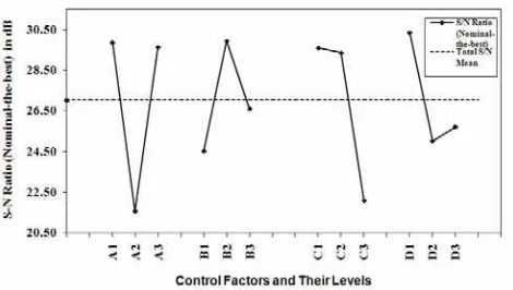
The effect of each process parameter on the S/N Ratio at different levels can be separated out because the experimental design is orthogonal. The S/N ratio (SNR) for each level of the process parameters is summarized in Table VII and Table VIII. In addition, the overall mean SNR for the nine experiments is also calculated and listed in Table VII and Table VIII.
TABLEVII
S/NRESPONSE FOR VTH IN PMOS DEVICE
S/N Ratio (dB) Symbol Process
Parameter Level
1 Level 2 Level 3
30.36 25.00 25.70 27.02
Parameter Level 1
74.30 74.39 74.39 74.36
0.09
Fig. 2 and Fig. 3 show the S/N ratio graphs of VTH and ILeak
for PMOS device respectively. Basically, the larger the S/N ratio, the quality characteristic for the threshold voltage and leakage current are better [7],[8]. The closer the quality characteristic value to the target, the better the product quality will be [16].
Fig. 3 S/N graph of leakage current for PMOS Device
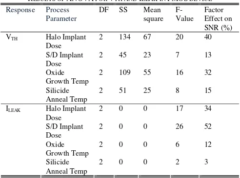
C.Analysis of Variance (ANOVA)
The analysis of variance (ANOVA) is a common statistical technique to determine the percent contribution of each factor for results of the experiment. It is also can be used to investigate which of the process parameters significantly affect the performance characteristics [11]. It calculates parameters known as sum of squares (SS), degree of freedom (DF), variance, F-value and percentage of each factor. The SS is a measure of the deviation of the experimental data from the mean value of the data. The total sum of squares can be calculated as [7],[17]:
(
)
2where n is the number of experiments in the orthogonal array,
ηi is the mean S/N ratio for the ith experiment and m is the
average of the nine ηi values. Similarly the SS for each factor
is sum of the square of average performance of a factor at each level, given by [7]
The degrees of freedom of the tested process parameter DF=t-1, where t the repetition of each level of the process
parameter, p. DF rather than the number of observation is used
in the variance calculation. The variance (mean square) of the process parameter tested is
DF SS
V p
p = [7],[10]. F-value for
each process parameter is the ratio of variance due to the effect of a factor and variance due to the error term,
e p
p V
V F = . It is used to measure the significance of the factor under
investigation with respect to the variance of all the factors included in the error term. Usually the larger the F-value, the effect on the performance characteristic is greater due to the change of the process parameter [17]. The percent contribution of each factor is the ratio of the factor sum to the total expressed in percent. For example, the percentage contribution ρ due to factor A can be calculated as [7]:
100
When the variance of the error is zero, the F-value for factors A, B, C and D is undetermined. Then the variance of the error can be combined with another smallest factor variance to calculate a new error variance which can be used to produce meaningful results. The process of disregarding an individual factor’s contribution and then subsequently adjusting the contribution of the other factor is known as pooling.
The results of ANOVA for the PMOS device are shown in Table IX. According to these analyses, factor A (halo implant dose) was found to be the major factor affecting the threshold voltage (40%), whereas factor B (S/D implant dose) was the major factor affecting the leakage current (52%). The percent factor effect on S/N Ratio indicates the priority of a factor (process parameter) to reduce variation. For a factor with a high percent contribution and a small variance (mean square) will have a great influence on the performance.
TABLEIX
In this research, factor C (oxide growth temperature) and factor A (halo implant dose) were found to be the second ranking factor affecting the threshold voltage (32%) and leakage current (34%) respectively. The analysis of average performance showed that the optimum condition is A1B1C1.
D.Confirmation of Optimum Run
The confirmation experiment is the final step in the first interaction of the design of the experiment process. The purpose of the confirmation experiment is to validate the conclusions drawn during the analysis phase17. Best setting of
the process parameters for PMOS device that effects on VTH
and ILeak , which had been suggested by Taguchi method is
shown in Table X.
TABLEX
BEST SETTING OF THE PROCESS PARAMETERS
Symbol Process Parameters Unit Best Value A Halo Implantation Dose atom cm-3 3.36E13
B S/D Implantation Dose atom cm-3 6.55E13
C Oxide Growth
Temperature
oC 815
D Silicide Anneal
Temperature
oC 900
Once the optimal level of the process parameters is selected, the final step is to predict and verify the improvement of the performance characteristic using the optimal level of the process parameters. The results of the final simulation for both parameters, VTH and ILeak are shown
in Tables XI and XII.
TABLEXI
RESULTS OF THE CONFIRMATION EXPERIMENT FOR VTH
Threshold Voltage (Volts) VTH1 VTH2 VTH 3 VTH 4
S/N Ratio (Nominal-the-Best) -0.1518 -0.1582 -0.1565 -0.1596 33.30
TABLEXII
RESULTS OF THE CONFIRMATION EXPERIMENT FOR ILEAK
Leakage Current (mA/μm) ILeak 1 ILeak 2 ILeak 3 ILeak 4
S/N Ratio (Smaller-the-Best)
0.192 0.196 0.196 0.195 74.21
The S/N ratios for VTH and Ileak after the optimization
approaches are 33.30 dB and 74.21 dB respectively. Both values are closer and within the predicted value. For VTH, 33.3
dB is closer to the predicted range S/N ratio of 32.99 to 32.83 dB (32.91 ± 0.08 dB). While for ILeak, 74.21 dB is within
predicted range S/N ratio 74.50 to 74.05 dB (74.27 ± 0.23 dB). These show that Taguchi Method can predict the optimum solution in finding the 45nm PMOS fabrication recipe with appropriate threshold voltage and leakage current values. The threshold voltage and leakage current for PMOS device after optimization approaches are -0.157V at ILeak=0.195mA/µm respectively. These values are exactly
same with International Technology Roadmap for Semiconductor (ITRS) prediction [15].
IV. CONCLUSION
As the conclusion, the optimum solution in achieving the desired transistor was successfully predicted by using Taguchi Method. Threshold voltage (VTH) is the main response in
determining whether the device works or not. Leakage current should also be kept as low as possible to increase the speed of the device by shortening the time to accumulate charge in the channel for a transistor to turn on. In this research, halo implant dose and oxide growth temperature are the most effective parameters with respect to the threshold voltage, whereas S/D implant dose is the most effective parameter that has the strongest effect on the leakage current for this device
ACKNOWLEDGMENT
The authors would like to thanks to the Ministry of Higher Education (MOHE) for their financial support, Photonic Lab Universiti Kebangsaan Malaysia (UKM) and Universiti Teknikal Malaysia Melaka (UTeM) for the moral support throughout the project.
REFERENCES
[1] Wong et. al., “CMOS scaling into the 21st Century: 0.1um and Beyond,” IBM J. Res. & Dev. 39, 112. 1995.
[2] Kang, Sung-Mo, Leblebici, Yusuf, “CMOS digital integrated circuit: analysis and design,” 3th Edition. New York: McGraw-Hill Higher Companies, Inc., 2003.
[3] S.M.Sze, “Semiconductor Devices: Physics and Technology,” 2nd
Edition, John Wiley & Sons Inc., 1986.
[4] S.Ninomiya et al., “Vth Control by Halo Implantation using the SEN's MIND System,” in Proc. 9th International Workshop on Junction Technology, 2009, pp. 100-103.
[5] Croon, J.A., Augendre, E., Decoutere, S., Sansen, W., Maes, H.E., “Influence of Doping Profile and Halo Implantation on the Threshold Voltage Mismatch of a 0.13μm CMOS Technology,” in Proc. 32th European Solid-State Device Research Conference (ESSDERC), Italy, 2002, pp. 579-582.
[6] Axel Erlebach, Thomas Feudal, Adreas Schenk, Christoph Zechner, “Influence of HALO and drain-extension doping gradients on transistor performance,” J. Materials Science and Engineering B, 114-115, 2004, pp. 15-19.
[7] Madhav S.Phadke, “Quality Engineering Using Robust Design,” Pearson Education, Inc. and Dorling Kindersley Publishing, Inc., 1998. [8] Ugur Esme. 2009. Application of Taguchi Method for the Optimization of Resistance Spot Welding Process, The Arabian Journal for Science and Engineering, Vol. 34, No. 2B
[9] G.P.Syros, J. Materials Processing Technology135, (2003), 68-74 [10] N.V.R.Naidu, “Mathematical model for quality cost optimization,
Robotics and Computer-integrated Manufacturing,” in Proc. International Conference on Flexible Automation and Intelligent Manufacturing, 2008, pp. 811-815.
[11] Kai Yang, Ee-Chon Teo and Franz Konstantin Fuss, “Application of Taguchi method in optimization of cervical ring cage,” J. Biomechanics, Vol. 40, 2007, pp. 3251-3256.
[12] H.Abdullah, J.Jurait, A.Lennie, Z.M.Nopiah and I.Ahmad, “Simulation of Fabrication Process VDMOSFET Transistor Using Silvaco Software,” European J. Scientific Research, ISSN 1450-216X, Vol.29
No.4, 2009, pp. 461-470.
[13] Ashok K. Goel, Matthew Merry, Kathryn Arkenberg, Eric Therkidsen, EmanuelChiaburu, William Standfest, “Optimization of Device Performance Using Semiconductor TCAD Tools,” Silvaco International, Product Description, Silvaco International, 2001.
[14] Belal Ahmed Hamida, Ibrahim Ahmad. 2007. “Optimization of PMOS 65nm Using Taguchi Method,” in Proc. International Conference on Modeling and Simulation, Coimbatore, 2007, August 27-29.
[15] ITRS Report (2007); http://www.itrs.net
[17] M.Nalbant, H.Gokkaya, G.Sur, “Application of Taguchi method in the optimization of cutting parameters for surface roughness turning,” J. Materials and Design, Vol. 28, 2007, pp. 1379-1385.
Fauziyah Salehuddin (M’76-SM’81-F’87) was born in N.Sembilan,
Malaysia, in 1969. She received the B.Sc. degree in electrical engineering from Universiti Teknologi Mara (UiTM), Malaysia in 2001 and the M.Sc. degree in Electrical, Electronic and System Engineering from Universiti Kebangsaan Malaysia, in 2003. Since December 2001, she has been with Universiti Teknikal Malaysia Melaka, working as lecturer. She is currently doing Ph.D. degree with Universiti Tenaga Nasional (UNITEN), Malaysia. Her Ph.D research, which is supervised by Prof. Dr. Ibrahim Ahmad, covered device and process simulation of nanoscale MOSFETs device and optimization of the process parameter variability on response characteristics in 45nm MOSFETs device.
Ibrahim Ahmad received the B.Sc. degree in Physics in 1980 from Universiti
Kebangsaan Malaysia (UKM). He received the M.Sc. degree in Nuclear Science and Analytical Physics from UKM and University of Wales respectively, in year of 1991 and 1992. He received the Ph.D. degree in Electrical, Electronic and System Engineering from Universiti Kebangsaan Malaysia in 2007. He was a Nuclear Science Officer at Nuclear Energy Unit (MINT) in charge of Radio scope production for medical and industry from 1987 to 1992. From 1993 to 1996, he worked on Semiconductor Technology Division at Malaysian institute for Microelectronics Research Center & System (MIMOS), Kuala Lumpur. He joint the Department of Electrical, Electronic and System Engineering, University Kebangsaan Malaysia (UKM) as a lecturer in 1997 to 2002, and as Associate Professor from 2002 to 2007. He involved in several management and technical positions with MINT, MIMOS, Emisis Smartkom Sdn. Bhd. K.Lumpur, Bumi Hibiya Sdn. Bhd. K.Lumpur and UKM. He is currently a Professor with the Department of Electronics and Communication Engineering, Universiti Tenaga Nasional, Malaysia. He published over 150 research papers in Journals and conferences. He is a senior member of the Institute of Electrical and Electronics Engineers (Senior MIEEE); Member of Institute of Physics Malaysia (MIPM) and Member of Malaysian Association of Solid States Science (MASS).
Fazrena Azlee Hamid received the BEng (Hons) degree in Electronic
Engineering from University of Southampton in 1999 and PhD degree (Electronic Engineering) from the same university in 2004. She is currently the Head of Unit (Academic) at the Department of Electronics and Communication Engineering, Universiti Tenaga Nasional (UNITEN). She joined UNITEN in 2004 as a lecturer and is currently a Senior Lecturer. Her research interest includes electronics design automation, analog and mixed-signal design, and engineering education. She is a member of IEEE and IET.
Azami Zaharim worked first 13 years as a lecturer in the Universiti
Teknologi MARA (University of MARA Technology - UiTM) before joining the Universiti Kebangsaan Malaysia (National University of Malaysia - UKM) in the year 2003. He is Associate Professor at the Faculty of Engineering and Built Environment UKM, and is currently the head for centre engineering education research. He obtained his BSc(Statistics and Computing) with Honours from North London University, UK in 1988 and PhD (Statistics) in 1996 from University of Newcastle Upon Tyne, UK. He specialize in statistics, public opinion, engineering education and renewable energy resources. He has until now published over 100 research papers in Journals and conferences, conducted more than 15 public opinion consultancies and delivered 3 keynotes/invited speeches at national and international meetings. He is currently the head of Renewable Energy Resources and Social Impact Research Group under the Solar Energy Research Institute (SERI). In the year 2007, he headed the Engineering Mathematics Research Group.
Husam Ahmed Elgomati was born in Tripole, Libya, in 1971. He received
the M.Sc. degree in Electrical, Electronic and System Engineering from Universiti Kebangsaan Malaysia, in 2005. He worked for 11 years at Libyan Telecommunication Company as one of Nano technology research group. Now, he is doing Ph.D. degree at Institute of Microengineering and Nanoelectronic (IMEN), Universiti Kebangsaan Malaysia. His Ph.D research, covered device and process simulation of nanoscale MOSFETs device and
MOSFETs device using Taguchi Method. He is currently one of the Institute of Micro engineering and Nanoelectronic member. His research interest includes Electronic Device and Nano technology
Burhanuddin Yeop Majlis is a professor of microelectronics and now the
Director of Institute of Microengineering and Nanoelectronics(IMEN). He received the Ph.D degree from University of Durham, UK in 1988. He received the M.Sc. degree from University of Wales, UK in 1980, and B.Sc.(Hons) from UKM in 1979. He is senior member of the Institution of Electrical, Electronics Engineers (SMIEEE) and fellow of Malaysian Solid State Science and Technology Soceity (FMASS). He received Johan Mangku Negara (J.M.N.) from Yang di-Pertuan Agong in 2008. Received Darjah Dato' Paduka Mahkota Perak (D.P.M.P.) from the Sultan of Perak
Prakash R.Apte obtained his B.E. in Electrical Engineering from Indore