Low Noise Amplifier for Front End Transceiver at 5.8 GHz
M.H Che Halim
1,M. Z. A. Abd Aziz,
2,A. Rani Othman1
3, S.A Sahingan
4 , M.F Selamat and 5,A.A
Abd Aziz
61 ,2,3,4,5,6
Faculty of Electronic & Computer Engineering, Universiti Teknikal Malaysia Melaka (UTeM)
Locked Bag 1200, Hang Tuah Jaya,75450, Ayer Keroh, Melaka,Malaysia,1
[email protected],[email protected],
3
[email protected],[email protected],[email protected], [email protected]
Abstract
This paper presents the design of 5.8 GHz front end Low Noise Amplifier application for IEEE standard 802.11 systems for WLAN application. Revolution and demand of WLAN technology have urged development of low cost, low power and small size transceiver by using microstrip technology [1]. This paper is present design and simulation of single stage LNA circuits. This paper is focusing on development of Low Noise Amplifier operating at 5.75-5.85GHz (5GHz upper U-NII band) for WLAN application. The amplifier design used FHX76LP Low noise SuperHEMT from Eudyna Device USA Inc. The transistor [2],[3]. The target simulation are gain (S21)
with >10dB, noise figure with <10dB and input and output return loss <-10dB at 5.8 GHz. A single stage LNA has successfully designed with 15.924 dB forward gain , 0.552 dB noise figure, -11.182 dB output return loss(S22) and -13.246 dB input return loss(S11) by using ADS software.
1. I
NTRODUCTIONThe IEEE 802.11 standard is used as references. The Low Noise Amplifier (LNA) system should meet this standard requirement and should operate properly for WLAN Bridge system [1]. The main requirements of the LNA are the lowest possible noise figure (NF) with a reasonable gain. The general topology of the LNA consists of three stages: the input matching network (IMN), the amplifier itself and the output matching network (OMN) [2],[3],[4]. The 5.8 GHz wireless LAN market
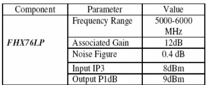
grows rapidly and offers various benefits to the user 5.8 GHz LAN technology supports multimedia services, real time voice and video transfer and other bandwidth intensive applications [5]. This paper presents two different designs of a LNA at 5.8GHz. The circuit design starts from FHX76LP Low noise SuperHEMT device designed for DBS application from Eudyna Device USA Inc amplifier using the microstrip technology. It is the LNA that mainly determines the noise figure of the system. Low power dissipation and small integrated area are also some important factors that must be considered in the design of the devices for wireless applications [6]. Based on S-parameters of the transistor and certain performance requirements, a systematic procedure is developed for the design of LNA. In LNA design, the most important factors are low noise, moderate gain, matching and stability [7]. Besides those factors, power consumption and layout design size also need to be considered in designed works.The characteristic of this commercialize Low Noise Amplifier are shows in Table 1 below
:-Table 1. FHX76LP characteristic
2. SINGLE STAGE LNA
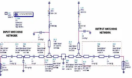
A single stage microwave transistor amplifier can be modeled by the circuit in Figure 1 where a matching network is used both sides of the transistor to transform the input and output impedance ZA to the
source and load impedance ZS and ZL. The most useful
2008 International Conference on Electronic Design December 1-3, 2008, Penang, Malaysia
gain definition for amplifier design is the transducer power gain, which accounts both source and load mismatch [4],[5],[6].
Figure 1: Single Stage LNA circuit
3. STABILITY CONSIDERATION
One of the most important factors in high frequency amplifier design is to determine stability of the given bias point. Equations in Table 2 and Table 3 are used to determine the stability and stability circle of the amplifier.
Table 2. Stability determination by formula
Table 3. Stability determinations by stability circle
The input and the output circuits should be matched to deliver maximum power to the load. After stability of active device is determined, input and output matching
circuits should be designed so that reflection coefficient of each port can be correlated with conjugate complex number as given below:
By combining the two formulas above, reflection coefficient of input/output matching circuits can be calculated by:
Where
4. NOISE FIGURE AND CONSTANT NOISE CIRCLE
Signals and noises applied to the input port of amplifier are amplified by the gain of the amplifier and noise of amplifier itself is added to the output. Therefore, SNR (Signal to Noise Ratio) of the output port is smaller than that of the input port. The ratio of SNR of input port to that of output port is referred to as noise figure and is larger or less than 1.Typically, noise figure of 2-port transistor has a minimum value at the specified admittance given by formula:
5. DESIGN FOR MINIMUM NOISE FIGURE
Low noise amplifier is important for receiver because noise figure of the amplifier of receiver affects noise figure of the whole system. To get minimum noise figure using 2-port transistor, source and load reflection coefficient should match with Γopt and load reflection coefficient should match with Γout with a complex conjugate number [9],[10] as formula
below:
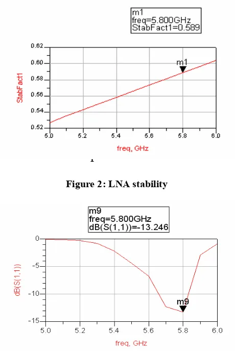
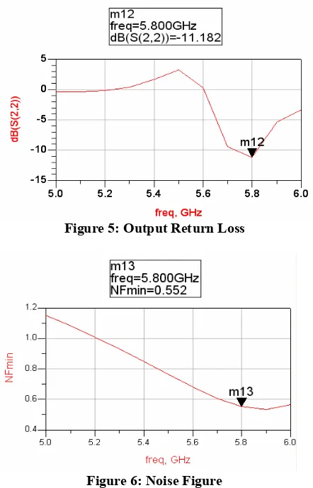
6. RESULT
For the proposed single stage LNA shown in Figure 1, the simulation result is shown in Figure 2 to Figure 6. The design LNA required two 2 V supply voltage and consumes 4.5mW. In the beginning of the simulation process, the transistor is modeled in schematic using data sheet provided by manufacturer. The simulation result might not be accurate because the library has no data and modeled of the transistor FHX76LP Low noise SuperHEMT in ADS software. However Duroid 5880 is being used as the microstrip substrate and the characteristic of this substrate. The comparison S-parameter simulated result as shown in Table 4.
F
Figure 2: LNA stability
Figure 3: Input Return Loss
Figure 5: Output Return Loss
Figure 6: Noise Figure
Table 4. S-parameter simulation result
A 5.8GHz low noise single stage amplifiers based on FHX76LP Low noise SuperHEMT transistor was designed and simulated by using ADS. At 2V collector bias on 5.8 GHz , this LNA has noise figure 0.552 dB, with input return loss of -13.246 dB, insertion loss of 21.503 dB and output return loss of -11.182 dB. Usually, as long as the stability factor and
The research work has yield a new Low Noise Amplifier (LNA) circuit design for frequency range of 5.75 GHz to 5.85 GHz and circuit simulation were done in ADS software. LNA has successfully simulated with 15.924 dB gain and 0.552 dB noise figures at frequency 5.8 GHz
REFERENCES
[1] Heng Jin and C.A.T. Salama, “A 1-V, 1.9- GHz CDMA, CMOS on SOI, low noise amplifier,” in
SOI Conference, 2000 IEEE International.
[2] T. Lee, The Design of CMOS Radio-Frequency
Integrated Circuits, Cambridge University Press,
1998.
[3] B. Jung Jang, I. Bok Yom, S. Pal Lee (2001). “V-Band MMIC Low Noise Amplifier Design Based on Distributed Active Device Model”, Proceedings of APMC2001, IEEE, 2001. 25-28.
[4] Sungkyung Park and Wonchan Kim, “Design of a 1.8 GHz low-noise amplifier for RF front-end in a 0.8,” Consumer Electronics, IEEE Transactions on, vol. 47, no. 0098, 2001.
[5] A. Parssinen, S. Lindfors, J. Ryynanen, S.I. Long, and K. Halonen, “1.8 GHz CMOS LNA with on-chip DCcoupling for a subsampling direct,” in Circuits and Systems, 1998. ISCAS ’98. Proceedings of the 1998 IEEE International
Symposium on, 1998, vol. 2, pp. 73–76.
[6] D.M. Pozar(2000). “Microwave and RF Wireless System”, United States of America: John Wiley and Sons Inc. 77-97, 205-207.
[7] G. Gonzalez (1997). “ Microwave Transistor Amplifier: Analysis and Design”, 2nd Edition, Upper Saddle River, NJ: Prentice – Hall Inc. 217, 294-303.
[8] D. M. Pozar (1998). “ Microwave Engineering”, 2nd Edition, United States of America: John Wiley and Sons Inc. 258-266, 600-605.
[9] T.K.K. Tsang and M.N. El-Gamal, “Gain and frequency controllable sub-1 V 5.8 GHz CMOS LNA,” in Circuits and Systems, 2002. ISCAS
2002. IEEE International Symposium on, 2002,