A Retrofit Circuit to Increase Output Power of
PV System During Partial Shading Condition
M. Z. Ramli, Z. Salam,
Member IEEE
Abstract -- In a typical photovoltaic (PV) distributed generation system, when part of the PV module is shaded, the bypass diode (that is connected in parallel to it) is used to protect the module from hot-spot damages. However, by employing this diode, the output power is reduced significantly because the power generated from the shaded module is totally unusable. Furthermore, when the current flows through the bypass diode, conduction losses occur which further degrade the system efficiency. In this paper, a simple retrofit circuit is proposed to increase the output power of PV system under partial shading condition. The idea is to utilize the current generated by the shaded module, detour it to a power electronics circuit and then process it to become part of the output power. Consequently, the inclusion of the retrofit circuit enables to system to deliver more power compared to the bypass diode method. Simulation results show marked improvement in the efficiency, especially under heavy partial shading condition.
Index Terms –Photovoltaic, Inverter, Partial Shading, bypass diode.
I.INTRODUCTION
or the past two decades or so, distributed power generation using renewable energy (RE) sources such as solar, wind, biomass and wave has attracted immense global interest. This is partly due to environmental concern, depleted fossil fuels and issues over energy securities. In particular, solar energy is envisaged to be an important RE source in the future because of the rapid reduction in the solar cell prices. The photovoltaic (PV) power system is starting to become a popular electrical power source due to its long term economic prospect and ease of maintenance due to the absence of moving components. DC power from the PV arrays (which are strings of PV modules in parallel and series connections) is converted to ac and connected to the grid distribution networks. Examples of large scale PV power systems can be found in many countries, for example, [1−6]
In a grid connected PV power system, the partial shading or unbalanced irradiation condition has been identified as the main reason that contributes to the output power reduction. This condition is caused by sudden cloud changes in the sky, obstruction of by tall buildings, trees, poles, towers etc. Another main cause of unbalance is the damage that occurs on
_______________________________________________________________ This work has been financially supported by the Universiti Teknologi Malaysia Vot number 68754
M.Z. Ramli is with the Universiti Teknikal Malaysia Melaka, 76109 Durian Tunggal,Melaka. Z.Salam (corresponding author) is with Faculty of Electrical Engineering, Universiti Teknologi Malaysia, 81310 Johor Bahru, Malaysia (e-mail: [email protected]).
one or several modules in the array. This may be in the form of physical module cracks, unintentional objects that landed on the module and un-uniform module degradation. Research conducted during the Germany’s 1000-Roofs PV Program confirmed that partial shading is the one of the main reason for reduction in energy yield [1]. This finding was supported by another field test program that was carried out in Japan [4].
Partially shaded arrays/modules create hot spots and can cause permanent damage of the shaded cell. In order to avoid this threat, a bypass diode is inserted in parallel to each module, which takes over the string current when the module is shaded. Although the impact of the shaded cells can be alleviated by inserting bypass diodes, partial shading still significantly impairs the energy yield of the overall system. This is because the shaded module, which may actually yield certain amount of power, is totally unusable. Furthermore, when the current flows through the bypass diode, conduction losses occur − further degrading the system efficiency.
For many years the most popular configuration PV power system is the series parallel (SP) combination of modules connected to a central inverter. In this configuration, a large number of PV modules are connected in series known as string. The advantages of using a large single central inverter are simplified monitoring, effective maintenance, lower system costs and higher system reliability [1]. The main drawback is that if one or more modules could not deliver power due to shading, multiple peaks in the I-V curve are created. If the maximum power point tracking (MPPT) algorithm is not sophisticated enough, there is a possibility for the MPPT unable to locate the real maximum point and settle at local peak. If this were to happen, the output power is of the PV system will be greatly reduced.
The Module Integrated Converter (MIC) is another approach for grid connected PV power system. Each module has its own “small” converter which is then chained together in parallel to form a larger system. Each converter consists of its own individual MPPT that tracks the maximum point of the module connected to it. Clearly it has the advantage of optimizing power output from each PV module independently. Although the concept is quite attractive, due to high number of converter to be connected in a large PV system, the cost and complexity of the system can be prohibitive.
required. The main advantages of the proposed retrofit circuit are:
• No power losses at during partial shading (theoretically). Power contribution by each module (including the shaded ones) is utilized.
• As opposed to MIC, only one MPPT circuit is required for the whole system.
• No switching losses during uniform irradiation condition.
• Low cost due to the simple switching scheme. The extra cost can be adsorbed by the extra power gained by the system during partial shading.
This paper describes the principle of operation of the proposed retrofit circuit. The concept is proven by a mixed-mode simulation using Matlab and Pspice.
II. THE RETROFIT CIRCUIT
A. General System
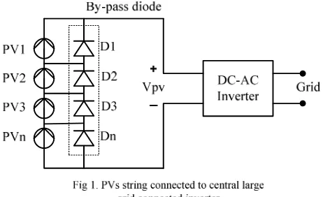
Figure 1 shows a typical PV power generation system using a central inverter. The depicted system is a single string array with n number of modules (PV1 through PVn). For each PV module, a bypass diode is connected in parallel to divert away the current when its associated module is shaded. This is necessary because if a module is shaded, it behaves like as a load instead of a generator. Current from other modules will be focused to the shaded module, creating a hot spot, which eventually destroy it.
B. The Proposed Retrofit Circuit
Fig. 2 shows the proposed retrofit circuit. As can be seen, the bypass diode for each module is absent. The basic concept of this topology is power from non-shaded modules is transferred to the shaded modules until all modules seem to have equal power level. Transferred energy then stored in the capacitors which are connected parallel with each module. From Fig. 3, four PV modules are connected in series. This topology can be divided into 3 groups of converter. Group 1 consists of S1, S2, D1, D2, L1, C1 and C2. Group 2 are S3, S4, D3, D4, L2, C3 and C4. Meanwhile, Group 3 consists of S5, S6, D5, D6 and L3.
The number of PV modules connected to the system can be extended by chaining more groups of converter. However the proposed topology can’t work alone without an interface converter in the middle. The purpose of an interface converter is to search the MPPT of the PV system. It can be any type such as DC-DC or DC-AC. In this work, boost converter was used.
The working principles of group 1 and 2 are identical: to transfer unbalanced power to each PV partner when non-uniform irradiation occurred. The group 3 operation is to transfer unbalanced power of group 1 and 2. The former group transferred the power when total irradiation of PV1 and PV2 is different with total irradiation of PV3 and PV4. As a result, all PVs have the same power level. During boost converter searching the MPPT, proper tuning of duty cycle value of all 3 groups of converter also have to be carried out at the same time. When the boost converter succeeded track the MPPT, all PVs were forced to operate at its own MPPT. Thus maximum power is transferred even during partial shading.
III OPERATING PRINCIPLE
A. Basic operating modes
To explain the circuit operation, the circuit of Group 1 is shown in the Fig 3. In essence, t is a bidirectional buck-boost converter. The PV1 is assumed will receive full irradiation, i.e. 1kW/m2 while PV2 is shaded at 50%. Therefore, PV1 has 50% more power than PV2. When S1 is at ON state, S2 is OFF. Duty cycle is set to 0.5. At this stage, the current flowed through S1, causing IL1 to increase linearly due to constant
voltage supply from PV1, V1.Energy is stored in inductor L1.
At stage 2, the diode D2 is conducted, energy in the inductor L1 is released and thus charging the capacitor C2. The charging and releasing energy process continue until both PVs and its capacitors have the same power level. As can be observed in the timing diagram shown Fig. 4, due to the utilization of the bidirectional switches, inductor current, IL1 is
!"#
$%!"#
&'
&
()*
B. Analysis
In order to analysis the DC characteristics of the proposed method, the shaded module (PV2) is replaced by a load resistor as shown in Fig. 5. At stage 1,
dt di L V
vL1= 1= 1
,
This will become:
( )
I closedL DT V
Δ =
1
1
(1)
And at stage 2,
dt di L V
vL1 =− 2= 1
,
Resulting in(
D)
T( )
I openL V
Δ = −
− 1
1
2 (2)
At the steady state operation:
( )
ΔI closed+( )
ΔI open =0.
(
1)
0 11
2
1 − − =
T D L V L
DT V
Therefore, the ratio V1/V2 can be express as:
) 1 (
2 1
D D V
V
−
= (3)
Setting the duty cycle to 0.5 will force the both V1 and V2 to be
at the same value. Therefore maximum power point can be achieved.
Load current, Idc is calculated as:
R V V
Idc= 1+ 2 (4)
Ptr is total power transfer from PV1 to PV2 during partial
shaded (note that PV2 is shaded). It can be written as:
2
2 1 1PV PV PV tr
P
P
P
P
=
−
−
(5)At steady state operation, power transfer from PV1 is equal to the power at the load, Ptr.
tr
L
D
P
I
V
I
V
1 1=
1 1=
Rearranging,D V
P
I tr
L 1
1= (6)
Ripple inductor current now can be calculated as:
1 1
1 1 1 min _ 1
2 L
DT V D V
P I I
I L tr
L
L = −
Δ −
= (7)
1 1
1 1 1 max _ 1
2 L
DT V D V
P I I
I L tr
L
L = +
Δ +
= (8)
Assuming all the ripple current component flows through the capacitor and its average current flows through the load resistor, the peak to peak voltage ripple can be written as:
C DT I C
Q
V o
r =
Δ = Δ
Since
2
V P I tr
o =
Then the ripple can be rearranged and rewritten as:
Cf V
D P V tr
r 2 =
From the equation (9) the voltage ripple,ΔVr is proportional to the amount of the power transferred, Ptr (all other parameter
are assuming fixed). This will be shown later in the simulation results. When the PV irradiation is heavily unbalanced due to heavy shading condition, ripple at PV output voltage will be large.
C. Simulation
A mixed mode simulation using Matlab-Simulink-Pspice was used to simulate this work. By using build in models uisng Pspice, the real switches power losses can be simulated.
S1
S2
S3
S4
S5
S6 L1
L2
L3 PV1
PV2
PV3
PV4 C1
C2
C3
C4
D1
D2
D3
D4
D5
D6
Vpv
L4 D6
RL C5
PI Controller Model Base
MPPT Tracking
Sun Irridiation Input
PV1 PV2 PV3 PV4
Vref
Fig 6: Simulation set-up to test the performance of proposed topology
Proposed Topology Boost Converter
S7
Fig. 6 shows the complete simulation set-up of the proposed topology together with the boost converter as an interface converter. The resistive load is also connected for completeness. The use of boost converter and a fixed resistive (instead of inverter and grid) is for simplicity. The concept proposed by the circuit can be easily extendable using an inverter.
A simple model based MPPT scheme was used due to the fast respond when irradiation condition is changing. In this algorithm, the data of PV MPPT points for the irradiation condition from 1kW/m2 to 0.1kW/m2 and the temperature 20ºC to 65ºC was stored. For a given solar irradiation and temperature inputs, the voltage reference, Vref at MPPT point
is then calculated based on that table.
The PV model based on the single diode was used [7−9]. Its governing behavior is described by Equation 10. The standard Newton Raphson iteration method was used to solve the equation.
p pv s pv nkT
R I V q
o ph pv
R
I
R
V
e
I
I
I
s pv
pv
+
−
¸
¸
¹
·
¨
¨
©
§
−
−
=
+
1
) ((10)
A PI controller is used to maintain the PV voltage, Vpv at the
voltage reference, Vref. The latter is computed by the MPPT
algorithm.
To make the simulation more realistic, the model parameters of PV BP-MSX60 module is used. It has the characteristics as shown in TABLE I.
TABLE I: SPECIFICATION OF BP-MSX-60 PV ARRAY
Maximum power (Pmax) 60W
Voltage at Pmax (Vmp) 17.1V
Current at Pmax (lmp) 3.5A
Minimum Pmax 58W
Short-circuit current (Isc) 3.8A Open-circuit voltage (Voc) 21.1V
IVRESULT
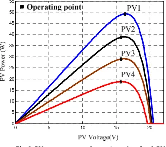
To simulate the partial shading condition, each PV modules was set the irradiation and temperature conditions as shown in TABLE II. To ensure that each module has a different voltage at MPPT, its surface temperature is randomly chosen with the assumption that a higher irradiation results in higher temperature. The true operating MPPT power is computed from the simulation and is shown in Table 2.
TABLE II: PV SHADING CONDITION AT DIFFERENT IRRADIATIONS AND TEMPERATURES
Irradiation (kW/m2)
Temp (ºC)
True MPP (W)
Operating MPP(W) PV1 1.0 35 51.30 49.20 PV2 0.8 33 40.28 38.72 PV3 0.6 28 29.46 28.95 PV4 0.4 25 18.92 18.67
Total power generated: 139.96W 135.54 W
Fig. 8 illustrates the MPPT operating point for each PV module under different irradiance. The values are obtained from Table 2. Fig. 9 shows the performance comparison between the proposed method and the standard bypass diodes modules. As can be clearly seen, be inserting the retrofit circuit, the system has recovered 35.54W or 25.4% more power than a system with a bypass diode. The time domain response of the power, current and output voltages at PVs terminal are shown in the Figs. 10 and 11. As can be observed, the proposed system responded very well to the changes of solar irradiation.
0 5 10 15 20
0 10 20 30 40 50 60 70 80 0
20 40 60 80 100 120 140
Proposed Method By-pass diode Method
Fig. 9: Simulation result of the total generated output power
Voltage (V)
T
o
tal Po
we
r (W
) 100W
135W
0 0.01 0.02 0.03 0.04 0.05 0.06 0.07 0.08
0 25 50 75 100
0 0.01 0.02 0.03 0.04 0.05 0.06 0.07 0.08
0 1 2 3 4
0 0.01 0.02 0.03 0.04 0.05 0.06 0.07 0.08
0 50 100 150 200
(a) Total PVs Output Voltage (b) Total PVs Output Current (c) Total PVs Output Power
(a)
(b)
(c)
Vo
lta
g
e (V)
C
u
rre
n
t (A)
Po
w
er
(
W
)
Fig. 10: Total PVs terminal voltage, current and power at the transient and steady state operation. Average solar irradiation change is 0.34kW/m2 which
is from 0.59kW/m2 to 0.93kW/m2.
0 0.01 0.02 0.03 0.04 0.05 0.06 0.07 0.08
0 5 10 15 20
0 0.01 0.02 0.03 0.04 0.05 0.06 0.07 0.08
0 5 10 15 20
0 0.01 0.02 0.03 0.04 0.05 0.06 0.07 0.08
0 5 10 15 20
0 0.01 0.02 0.03 0.04 0.05 0.06 0.07 0.08
0 5 10 15 20
PV1
PV2
PV3
PV4
V
o
lt
ag
e(
V
)
V
o
lt
ag
e(
V
)
Vo
lt
ag
e
(V
)
V
o
lt
ag
e(
V
)
Time(s)
Fig. 11: Individual PVs terminal voltage at the transient and steady state.
To investigate the switching and conduction power losses, the net power generated by proposed method is compared with system with two different methods, i.e. (1) with bypass diode and (2) Module Integrated Converter (MIC). The latter is the topology that connects one boost converter for each PV module. For this type, each converter is equipped with its own MPPT. Therefore ach module is operated at its maximum
point, even if it is shaded. For accuracy, switches models with losses are selected from pre-install Pspice software library. Five different irradiation patterns are designed and for each condition, its irradiance combination is shown in TABLE III. The overall efficiency (output power delivered by the system divided by the input power) calculated from all three methods is shown in Fig. 12.
TABLE III: PVS IRRADIATION CONDITION (KW/M2) AT TEMPERATURE 25ºC
Condition PV1 PV2 PV3 PV4
1 1.00 1.00 1.00 1.00
2 1.00 0.50 1.00 0.50
3 1.00 0.80 0.60 0.40
4 0.80 0.80 0.50 0.30
5 1.00 0.4 0.30 0.20
50 55 60 65 70 75 80 85 90 95 100 105
1 2 3 4 5
Irridiation Conditions
E
ffi
ci
en
cy
(%
)
Bypass Diode Individual Boost Proposed Method
Fig. 12: Overall efficiency comparison of different MPPT algorithm during partial shading condition show in Table 2.
From the histogram in Fig. 12, it can be observed that the bypass diode method has the highest efficiency when all PVs were in the uniform (normal) irradiation condition. However, when one or more modules are shaded, its efficiency drops significantly. It becomes worst for condition 5 (which is the most severe shading case) which is only 55% of the input power is delivered to the output. The reason for this low efficiency is the possibility that the MPPPT algorithm could not converge to the global point; rather it traps in on the local maxima. On the other hand, the proposed method achieves an average efficiency of more than 95% for all shading condition. It appears that the shading pattern has very little effect on the performance of the retrofit circuit. For the MIC, the average efficiency is only 90% despite the fact each individual boost has its own MPPT. This is due to the fact that in the MIC, the full PV current will pass through the boost switches, increasing the total losses. Meanwhile, in the proposed topology, only the current of shaded module will passed through retrofit circuit. The rest of the current will flow through the series PV connection. Consequently the conduction loss is reduced.
V.CONCLUSIONS
take the current from the shaded module, detour it to a power electronics circuit and process it to become part of the output power. Consequently, the inclusion of the retrofit circuit enables to system to deliver more power compared to traditional bypass diode method. Simulation results show marked improvement in the output power, especially under heavy partial shading condition. The comparison is based on simulation done on bypass diode and Module Integrated Converter. The extra power generated is expected to compensate for the cost of the extra components in the retrofit circuit and generates profit in the long run.
VIACKNOWLEDGEMENTS
This work has been financially supported by the Universiti Teknologi Malaysia Vot number 68754.
VIIREFERENCES
[1] Myrzik, J.M.A.; Calais, M.; , "String and module integrated inverters for single-phase grid connected photovoltaic systems - a review," Power Tech Conference Proceedings, 2003 IEEE Bologna , vol.2, no., pp. 8 pp. Vol.2, 23-26, June 2003
[2] Miyatake, M.; Toriumi, F.; Endo, T.; Fujii, N.; , "A Novel maximum power point tracker controlling several converters connected to photovoltaic arrays with particle swarm optimization technique," Power Electronics and Applications, 2007 European Conference on , vol., no., pp.1-10, 2-5 Sept. 2007
[3] Ramaprabha, R.; Mathur, B.; Ravi, A.; Aventhika, S.; , "Modified Fibonacci Search Based MPPT Scheme for SPVA Under Partial Shaded Conditions,"Emerging Trends in Engineering and Technology (ICETET), 2010 3rd International Conference on , vol., no., pp.379-384, 19-21 Nov. 2010
[4] Kurokawa, K.; Sugiyama, H.; Uchida, D.; Sakuta, K.; Sakamoto, K.; Ohshiro, T.; Matsuo, T.; Katagiri, T.; , "Extended performance analysis of 70 PV systems in Japanese field test program," Photovoltaic Specialists Conference, 1997., Conference Record of the Twenty-Sixth IEEE , vol., no., pp.1249-1252, 29 Sep-3 Oct 1997
[5] Di Piazza, M.C.; Pucci, M.; Ragusa, A.; Vitale, G.; , "Fuzzified PI voltage control for boost converters in multi-string PV plants," Industrial Electronics, 2008. IECON 2008. 34th Annual Conference of IEEE , vol., no., pp.2338-2345, 10-13 Nov. 2008
[6] Kjaer, S.B.; Pedersen, J.K.; Blaabjerg, F.; , "A review of single-phase grid-connected inverters for photovoltaic modules," Industry Applications, IEEE Transactions on , vol.41, no.5, pp. 1292- 1306, Sept.-Oct. 2005.
[7] K. Ishaque, Z. Salam, H. Taheri, Syafaruddin, Modeling and simulation of photovoltaic (PV) system during partial shading based on a two-diode model, Simulation Modelling Practice and Theory, 19 (2011) 1613-1626, 2011.
[8] K. Ishaque, Z. Salam, H. Taheri, Simple, fast and accurate two-diode model for photovoltaic modules, Solar Energy Materials and Solar Cells, 95 (2011) 586-594, 2011.
[9] K. Ishaque, Z. Salam, “An improved modeling method to determine the model parameters of photovoltaic (PV) modules using differential evolution (DE)”, Solar Energy, Vol. 85, Issue 6, pp. 2349-2359, 2011.
IVBIOGRAPHIES
Mohd Zulkifli Ramli was born in Terengganu, Malaysia in 1978. He received both B. Sc. degree and M. Eng Degree from Universiti Teknologi Malaysia (UTM) in 2000 and 2004, all in electrical engineering. He is currently pursuing his PhD in Photovoltaic areas at the same
University. His primary interests are in the Inverter, DC-DC converter and photovoltaic.
Zainal Salam obtained his B.Sc., M.E.E. and Ph.D. from the University of California, Universiti Teknologi Malaysia (UTM) and University of Birmingham, UK, in 1985, 1989 and 1997, respectively.
He has been a lecturer at UTM for 25 years and is now a Professor in Power Electronics at the Faculty of Electrical Engineering. He has been working in several researches and consulting works on battery powered converters, solar energy and machine control. Currently he is the Director of the Inverter Quality Control Center (IQCC) UTM which is responsible to test PV inverters that are to be connected to the local utility grid. His research interests include all areas of power