ContentslistsavailableatSciVerseScienceDirect
Applied
Surface
Science
jo u r n al h om ep a g e :w w w . e l s e v i e r . c o m / l o c a t e / a p s u s c
Experimental
investigation
on
material
migration
phenomena
in
micro-EDM
of
reaction-bonded
silicon
carbide
Pay
Jun
Liew
a,c,
Jiwang
Yan
b,∗,
Tsunemoto
Kuriyagawa
aaDepartmentofMechanicalSystemsandDesign,TohokuUniversity,AramakiAoba6-6-01,Aoba-ku,Sendai,980-8579,Japan
bDepartmentofMechanicalEngineering,FacultyofScienceandTechnology,KeioUniversity,Hiyoshi3-14-1,Kohoku-ku,Yokohama,223-8522,Japan cManufacturingProcessDepartment,FacultyofManufacturingEngineering,UniversitiTeknikalMalaysiaMelaka,HangTuahJaya,76100,DurianTunggal,
Melaka,Malaysia
a
r
t
i
c
l
e
i
n
f
o
Articlehistory:
Received15December2012
Receivedinrevisedform23March2013 Accepted25March2013
Available online 2 April 2013
Keywords:
Microelectrodischargemachining Materialmigration
Materialdeposition Carbonnanofibre
Reaction-bondedsiliconcarbide Tungstenparticle
a
b
s
t
r
a
c
t
Materialmigrationbetweentoolelectrodeandworkpiecematerialinmicroelectricaldischarge machin-ingofreaction-bondedsiliconcarbidewasexperimentallyinvestigated.Themicrostructuralchangesof workpieceandtungstentoolelectrodewereexaminedusingscanningelectronmicroscopy,cross sec-tionaltransmissionelectronmicroscopyandenergydispersiveX-rayundervariousvoltage,capacitance andcarbonnanofibreconcentrationinthedielectricfluid.Resultsshowthattungstenisdeposited inten-sivelyinsidethedischarge-inducedcratersontheRB-SiCsurfaceasamorphousstructureformingmicro particles,andonflatsurfaceregionasathininterdiffusionlayerofpoly-crystallinestructure.Deposition ofcarbonelementontoolelectrodewasdetected,indicatingpossiblematerialmigrationtothetool elec-trodefromworkpiecematerial,carbonnanofibresanddielectricoil.Materialdepositionratewasfoundto bestronglyaffectedbyworkpiecesurfaceroughness,voltageandcapacitanceoftheelectricaldischarge circuit.Carbonnanofibreadditioninthedielectricatasuitableconcentrationsignificantlyreducedthe materialdepositionrate.
© 2013 Elsevier B.V. All rights reserved.
1. Introduction
Inrecentyears,theuseofceramicsinmechanicaland manu-facturingengineeringhasreceivedintensiveattention,duetotheir outstandingmaterialproperties.However,becauseoftheirhigh hardness,ceramicsaredifficulttobeformedtocomplexgeometries bytraditionalmachiningprocesses[1].Recently,theuseof electri-caldischargemachining(EDM)tomachineceramicshasbecomea newresearchfocus,owingtoitsadvantagessuchaslow installa-tioncostandabilitytomachinecomplexthree-dimensionalshapes easilyregardlessofmaterialhardness[2].
Many previousstudieshavebeen conductedtoimprovethe machining efficiency and accuracy of ceramics by using EDM, andgreatprogresshasbeenmadeinthisarea.Pioneerworkcan betraced toMohriet al.[3], whoreported thatthemachining ofinsulatingceramicscanberealizedinEDMbyassisting elec-trodemethod.Liu etal. [4]employeda steel toothedwheelas thetoolelectrodetomachinehighresistivitySiCceramicsusing electricaldischargemilling.ThefeasibilityofEDMformachining non-conductiveceramicsZrO2 andAl2O3 usingadherentcopper foilwasconductedbyLinetal.[5].Fukuzawaetal.[6]andClijsters
∗Correspondingauthor.Tel.:+81455661445;fax:+81455661495.
E-mailaddress:[email protected](J.Yan).
etal.[7]fabricatedthree-dimensionalcomplexshapesuccessfully onceramicsbyEDM.Acomparativestudyofthedie-sinkingEDM ofthreedifferentceramicmaterialshasbeencarriedoutbyPuertas andLuis[8].
However,afewproblemsstillexistwhichlimittheapplication ofEDMtechnologytohighvalue-addedmanufacturingindustries. Forexample,theEDMfabricatedsurfaceisquiteroughduetothe electricaldischargeinducedcraters.Themeltingand resolidifica-tionofmaterialcausessurfacepropertychangeoftheworkpiece material. Another problem is that during electrical discharges, materialmigrationsoccurfromtheelectrodetotheworkpiece[9]. Thematerialmigrationleadstodepositionoftoolmaterialtothe workpiecesurface,causingsurfacecontamination.Especiallywhen performingEDMin themicro/nanoscale, theeffectofmaterial migrationmayplayanimportantrolefromviewpointof mechan-icalandphysicalpropertiesofthemachinedsurface.
Thematerialmigration phenomenon inEDMhasbeen stud-iedby manypreviousresearchers. For instance,electroerosion of various metal materials,such asA1, Cr, Cu, Fe,and Zn, has beeninvestigatedbyGreeneandGuerrero-Alvarez[10].Jeswani andBasu[11]studiedthedepositionanddiffusionofcopperand brasstoolmaterialsonmildsteel,highcarbonsteelandhighspeed steel.SoniandChakraverti[12]reportedthechangeinchemical compositionduetothemigrationofcopper–tungstentool mate-rialtoworkpieceduringEDMofdiesteel.Thematerialmigration
phenomena in EDM using suspended powder [13,14], powder compactand multi-layerelectrodes[15–17]andcombinationof powder and powder metallurgy electrode [18] have also been investigated.Murrayetal.[19]reportedreverse-direction mate-rial migration, i.e., the attachment of workpiece debrison the toolelectrodes.Apartfromthematerialtransferbetweenthetool and workpiece,Mafarona [20] and Jahan etal. [21] found that anamountofcarbonmigratestobothtool electrodeand work-pieceduetothedecompositionofdielectricfluid.Kruthetal.[22], Ekmekci[23] andThomson [24]showedthat thecarbon inthe whitelayeronmachinedsurfacemainlycomesfromthe hydro-carbonbaseddielectricfluid.However,mostofthepreviousworks havefocusedonmaterialmigrationinEDMofhighconductivity materials,whereasthereisnoavailableliteratureonthatof low-conductivityceramicmaterials.
Inarecentpaperofthepresentauthors[25],wecarriedout microEDMexperimentsonreaction-bondedsiliconcarbide (RB-SiC), an important ceramic material which has extremely low electricalconductivity.Wefoundthatbyaddingcarbonnanofibres inthedielectricfluid,theEDMcharacteristicsweresignificantly improvedintermsofmaterialremovalrate,machinedsurface qual-ityandtool electrodewear.Thistechnologyprovidespossibility forhigh-efficiencyprecisionmanufacturingofmicrostructureson ultra-hardceramicmaterials.However,thematerialmigrationin microEDMofRB-SiCanditseffectsonthemachiningprocessis stillunknown.Therefore, inthis work,weaimedtoinvestigate thematerialmigrationphenomenonduringthemicroEDMof RB-SiCandtoclarifyitsfundamentalmechanism.Thefinalobjective istofindoptimalconditionstocontrolthematerialmigrationin microEDMofceramicmaterialsandtoimprovethefinishedsurface topographyandsurfaceintegrity.
2. Experimentalmethods
2.1. Equipmentandmaterials
TheexperimentswerecarriedoutusingamicroEDMmachine PanasonicMG-ED82W.ThismachinehasaResistor–Capacitor(RC) dischargecircuit,withasteppingresolutionof0.1m.Fig.1shows aschematicdiagramoftheexperimentalsetup.
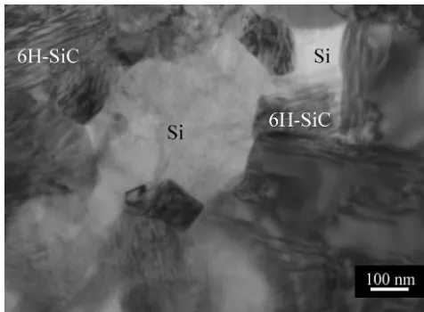
RB-SiC ceramic with electrical resistivity (∼1453cm) pro-ducedbyJapanFineCeramicsCo.,Ltd.wasselectedasworkpiece material.TheRB-SiCmaterialcomposedof6H-SiCgrains (aver-agesize<1m)andaSimatrix(approximately10%involume). BeforeEDMexperiments,thesurfacemicrostructuresoftheRB-SiC ceramicwereexaminedusingtransmissionelectronmicroscopy (TEM),aspresentedinFig.2.IntheTEMmicrograph,darkgrey
R
C
DC
V
Workpiece
(+ve)
Electrode
(-ve) Tool
electrode
rotation
Fig.1.SchematicdiagramoftheEDMexperimentalsetup.
Fig.2. MicrostructuresofRB-SiCobservedbyTEM.
Fig.3. SEMmicrographoftungstengrain.
grainsare6H-SiCandthelightgreyregionsaroundthemare inter-grainSibonds(sizelessthan1m).Itisnoticedthatafew6H-SiC grainsaredirectlybondedtoeachotherwithoutthepresenceofSi bondsatthegrainboundaries,resultinginaverydensestructure.
Tungstenrodswith300mdiameterswereusedastool elec-trodes.Acrosssectionsampleofatungstenelectrodewasprepared usingionmillingandwasobservedusingSEM,asshowninFig.3. Itshowsthatmostofthegrainsoftungstenarelongandthin,the averagesizeofwhichisabout1m.Theelectrodeswereformed intohemi-sphericalshapeswith100mradiibythewire electri-caldischargegrinding(WEDG)unitequippedintheexperimental setup.Sometypicalmaterialpropertiesoftheworkpieceandthe electrodearelistedinTables1and2,respectively.
Table1
MaterialspropertiesofRB-SiC(workpiece)[26].
Properties Values
Grainsize(m) <1
Volume(%) Si-12,6H-SiC-88
Density(g/cm3) 3.12
Softeningtemperature(◦C) 1375
Electricalresistivity(cm) ∼1453
YoungmodulusE(GPa) 407
Vickershardness(GPa) 25–35
Table2
Materialspropertiesoftungsten(electrode)[27].
Properties Values
Grainsize(m) ∼1
Volume(%) 99.9
Density(g/cm3) 19.3
Meltingtemperature(◦C) 3380
Electricalresistivity(cm) 5.65×10⁻⁶
YoungmodulusE(GPa) 411
Vickershardness(MPa) 3430
Thermalconductivity(W/mK) 173
2.2. EDMconditions
EachmicroEDMtestwasperformedonthesampleforduration of3min,andaverageofthreetestsforeachparametersettingwas taken.EDMoilCASTY-LUBEEDSwasusedasdielectricfluidfirst, andthencarbonnanofibreswereaddedintotheEDMoilatdifferent concentrationsforcomparison.Thevoltageandcapacitanceofthe electricaldischargecircuitwerechanged,andtheextentofmaterial migrationsbetweenthetoolelectrodeandtheRB-SiCworkpiece wasinvestigatedexperimentally.Theexperimentalconditionsare summarizedinTable3.
Table3
Experimentalconditions.
Workpiecematerial RB-SiC
Electrodematerial Tungsten
Polarity Positive(workpiece)
Negative(tool)
Rotationalspeed(rpm) 3000
Feedrate(m/s) 3
Voltage(V) 60–110
Condensercapacitance(pF) straycapacitance(∼1),10,110,
220,3300
Dielectricfluid EDMoilCASTY-LUBEEDS
Additive CNFsize(m) Concentration(g/L)
Carbonnanofibre(CNF) diameter=0.15,length=6–8 0.06–0.28
Machiningtime(min) 3
2.3. Characterization
Inordertoexaminethemicrostructureofthesamples,surface topographyofthemachinedmicrocavitywasexaminedusingSEM. Subsequently,energydispersiveX-ray(EDX)wasusedtodetect materialmigrationandmeasuretheamountofmigratedmaterial. TalymapsoftwaredevelopedbyTaylorHobsonLtd.,UK[28],was usedtoprocesstheSEMphotographtoquantifythesizeofmigrated particles. In order to clarify the microstructures of migrated material,thecrosssectionsofmachinedmicrocavitiesandtool electrode tips were observed using TEM. Mechanical polishing andfocusedionbeam(FIB)techniqueswereusedtopreparethe TEMsamples.
3. Resultsanddiscussion
3.1. Materialdepositionphenomena
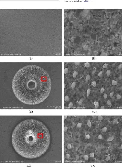
In the experiments, we found that the finished surface of RB-SiCiscoveredbysmallparticlesafterEDMunderafew con-ditions.For example, Fig.4(c) and (e) shows SEM micrographs ofmicrocavitiesobtainedunderfinemachiningconditions (volt-age80V, stray capacitance ∼1pF) with/withoutadding carbon nanofibres in dielectric oil, respectively. In the figure, (d) and (f)arehigh-magnificationviewsofthemicrocavitiesin (c)and (e),respectively.It can beseen thatfor both machining condi-tions,lotsofsmallwhiteparticles(size∼1m)havebeenformed on the machined surface, which are uniform in size and dis-tribution.Since thesewhiteparticlesdidnot appearbeforethe EDMtests,asdepictedinFig.4(a)and(b), wecansaythatthe particleshavebeengeneratedduringEDMduetomaterial migra-tion and deposition on the machined surface. In Fig. 4(c) and (e),coneshape protrusionsare seenatthecentre of themicro cavities,which werecaused bythedecentringofthetool elec-trodes.
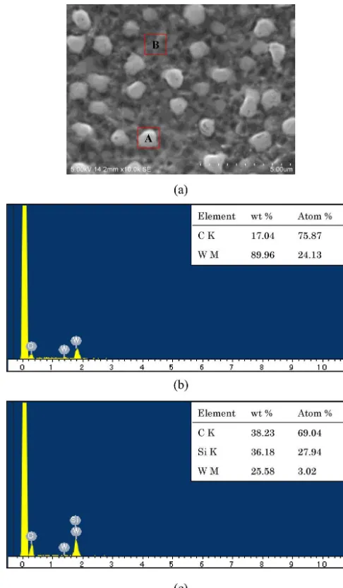
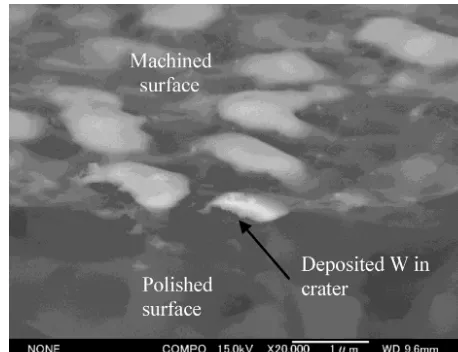
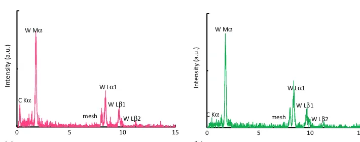
In orderto confirmtheelemental composition of thewhite particles,themachinedsurface wasanalyzedusingEDXat two differentlocations,particleregionAandparticle-freeregionB,as indicated inFig.5(a).Asshown in Fig.5(b), theEDX spectrum forZone A consistsof tungsten(W)at highweightpercentage (89.96%).Thisresultdemonstratesthatthewhiteparticlesonthe machinedsurfacearemainlytungsten,whichhasbeenmigrated fromthetool electrode anddepositedonthemachinedsurface during the micro EDM process. In Zone B, tungsten was also detectedbuttheweightpercentageislow(25.58%),asdepicted inFig.5(c).Thesilicon(Si)elementinthespectrashouldbefrom theparentmaterialRB-SiC,andthecarbon(C)elementmightbe
Fig.5. (a)SEMmicrographofthelocationmappedbyEDX(b)EDXspectrumanalysis atzoneA(c)EDXspectrumanalysisatzoneB.
fromtheparentmaterialRB-SiC and/ortheCNFsinthe dielec-tric.
3.2. Effectofvoltage
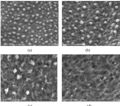
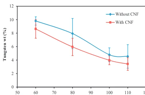
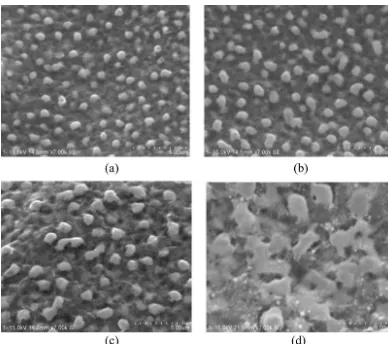
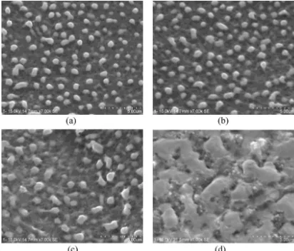
Figs.6and7presentSEMmicrographsofmachinedRB-SiC sur-facesat differentvoltages from60V to110Vunder conditions with/withoutcarbonnanofibresaddition,respectively.Whenalow voltage(60V)wasused,thequantityofthedepositedtungsten par-ticlesishigh,asshowninFigs.6(a)and7(a).However,asthevoltage increases(110V),thedepositedtungstenparticlesreducerapidly, asshowninFigs.6(d)and7(d).Fig.8showschangesintungsten weightpercentagewithvoltage.Itcanbeseenthatforboth con-ditions(with/withoutcarbonnanofibres),theweightpercentage ofdepositedtungstenmaterialdecreasessignificantlyasvoltage increases.
Fig.6. MachinedsurfaceatstrayCbutdifferentlevelsofvoltagewithcarbonnanofibresaddition:(a)60V(b)80V(c)100V(d)110V.
voltage, the gap between the tool and workpiece is very small.Therefore,theelectricaldischarge-inducedtungstendebris cannot be removed effectively from the gap, and instead, be deposited on the machined surface. However, when the voltageincreases,thesparkgapbecomeslarger.Thismakes flush-ingoftungstendebriseasier,resultinginadecreaseinmaterial deposition.
In Fig. 8, it is worth noting that by using carbon nanofi-breadditive, tungstenmaterial depositionbecomes lower than that obtained with pure dielectric fluid. When carbon nanofi-bres are added intothe dielectric fluid, theinsulating strength of dielectric fluid will be reduced, causing a bigger discharge gap between thetool electrode and the workpiece [25]. Thus, tungstendebriswillbeflushedouteffectivelyfromthegapand depositionwillbeprevented. Thisresultstrongly demonstrates that adding carbon nanofibres in the dielectric fluid is helpful for preventing electrode material deposition on the machined surface.
3.3. Effectofcapacitance
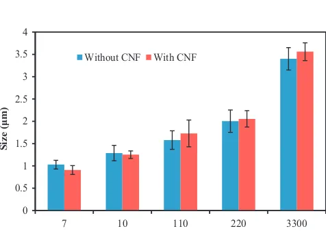
Next,theeffectofcapacitanceondepositionoftungstentool materialonmachinedsurfacewasinvestigated.Figs.9and10show SEMmicrographsofthemachinedsurfacebymicroEDMobtained with/withoutcarbonnanofibresaddition,respectively.The capaci-tancerangedfromstraycapacitance(∼1pF)to3300pFataconstant voltageof60V.Itisseenthatthesizeofthedepositedparticles
increaseswhenhighercapacitanceisused.Afewdeposited tung-stenparticles tendtocombinetoeachotherin thecapacitance rangefrom110pFto3300pF.
Thesizeofthedepositedtungstenparticleswasthenmeasured byTalymapsoftware.Anexampleofparticlesizemeasurementis showninFig.11.Fig.12showsthechangeinsizeofthedeposited tungstenparticleswithcapacitance.Itisseenthattheparticlesize increaseswiththecapacitanceforbothconditionswith/without carbon nanofibres. This is consistent withthe change in tung-stenweightpercentageanalyzedbyEDX,asshowninFig.13.It isknownthatcapacitancehadlesseffectonthemachininggap thanthevoltagedid[29].However,thehigherthecapacitanceis, thelongerthedischarge duration is[9]. Therefore, theamount ofmigrationanddepositionoftoolmaterialwillbehigherwhen longerdischargedurationisused,providedthatthemachininggap isconstant.
Fig.7. MachinedsurfaceatstrayCbutdifferentlevelsofvoltagewithoutcarbonnanofibresaddition:(a)60V(b)80V(c)100V(d)110V.
werelowerwiththeuseofcarbonnanofibresbelow10pF.This indicates that there might be a range of capacitance between 10pFand 110pFwhere theuseof carbonnanofibres andpure dielectricoilmakenodifferenceonthesizeofparticleand depo-sitionrate.Unfortunately, theverification of thisissue wasnot currently supported by the present experimental setup of the authors.
3.4. Effectofcarbonnanofibreconcentration
Fig. 14 illustrates the effect of carbon nanofibre concen-tration on the weight percentage of deposited tungsten material. The weight percentage of deposited tungsten material decreases with the carbon nanofibre concentration until0.06g/L.Astheconcentrationincreasesfurther,thematerial deposition tends to increase. As carbon nanofibre concentra-tion increases beyond 0.20g/L, material deposition decreases again. It is noteworthy that the trend of material deposition in Fig. 14 is very similar to that of the surface roughness as we demonstrated in our previous paper [25]. This fact indicates that tool material deposition is affected by surface roughness.Asthetungstendebrisiseasytobedepositedinthe cratersonthemachinedsurface,thesmallerthecratersizeis(the lowerthesurfaceroughnessis),thelowerthematerialdeposition
is[31].Fromthismeaning,itispresumablethatbyusingasuitable amountofcarbonnanofibres,surfaceroughnesswillbeimproved and tungsten material deposition could be prevented. In the presentstudy,theoptimum concentrationis 0.06gofCNFsper litrecapacityofthedielectricfluid(EDMoilCASTY-LUBEEDS).
0 2 4 6 8 10 12
50 60 70 80 90 100 110 120
T
un
gs
ten
wt
(
%)
Voltage (V)
Without CNF
With CNF
Fig.9.Machinedsurfaceatthesamevoltage60Vbutdifferentlevelsofcapacitancewithcarbonnanofibresaddition:(a)strayC(b)10pF(c)110pF(d)3300pF.
3.5. Cross-sectionalTEMobservation
Toexaminethemicrostructuresofthedepositedmaterial,the machinedsurfacewascross-sectionedbymechanicalpolishingand FIB,andobservedbySEMandTEM,respectively.Fig.15showsSEM micrographofmachinedsurfaceafterpolishingofthecrosssection. Itisseenthatwhitetungstenparticleswithanaveragesizearound 1mweredepositedinsidethecratersonthemachinedsurface. Afewtungstenparticlesmighthavebeenremovedpartiallyfrom thesurfaceduringpolishing,leavingresidualwhitelayers.
Fig.16isacross-sectionalTEMmicrographofamicrocavity machinedat70Vandstraycapacitance(∼1pF).Itisseenthat tung-stenparticles(blackregionA)werefirmlydepositedinthecrater oftheworkpiecewhichiscomposedof6H-SiCandSigrains.On thesurfacewhereWparticleswerenotdeposited,adarklayerof material(regionB)withathicknessofapproximately40–50nmis formed,thecompositionsandmicrostructureofwhichlooks dif-ferentfromthebulkmaterial.Toconfirmthemicrostructureofthe depositedparticleanddarklayer,electrondiffractionanalysiswas doneusingtheTEM,asshowninFig.17.InFig.17(a),onlyfuzzy ringsareshown,indicatingthatthedepositedtungsteninZoneA hasanamorphousstructure.Incontrast,inFig.17(b),aseriesof concentricringsresultingfrommanydiffractionspotsalsocanbe seen,demonstratingthatthedepositeddarklayeronthemachined surfaceispoly-crystalline.
Similar amorphous/poly-crystalline layers on bulk materials havealsobeenobservedinmechanicalmachiningprocesses.For example,inthediamondturningofRB-SiC[32],amorphizationof siliconmatrixanddislodgementofSiCgrainswereconfirmed.In diamondcuttingofsinglecrystallinesilicon[33],anamorphous layerwitha thicknessrangingfromthenanometreleveltothe submicron level was formed onthe workpiece surface. In sin-glepointdiamondturningofsingle-crystalSiC(6H)[34],original single-crystal SiCmaterial wastransformedinto anamorphous material,onthesurfaceandwithinthechip.Subsurface deforma-tionofvarioustypesofsinglecrystalSiCwasalsoconfirmedin moleculardynamicssimulationofnanometrelevelcutting[35], and the subsurface crystal lattice deformedlayer depths were quantifiedby subtractingtheuncut chipthickness.However,it shouldbenotedthatinthisstudy,theamorphous/poly-crystalline layerisdepositedontheworkpiecefromthetoolelectrodeand not phase-transformed from the bulk material by mechanical stresses.Fromthismeaning,wecansaythattheformation mech-anismofthesubsurfacelayerinthisworkisdistinctlydifferent fromthoseinmechanicalmachiningprocessessuchasdiamond turning.
Fig.10.Machinedsurfaceatthesamevoltage60Vbutdifferentlevelsofcapacitancewithoutcarbonnanofibresaddition:(a)strayC(b)10pF(c)110pF(d)3300pF.
Fig.18(b),besidestungsten(W),carbon(C)andsilicon(Si)were alsofound,indicating thattheinterdiffusionoftungsten,silicon andcarbonmighthaveoccurred.Thesecross-sectionalEDXresults agreewellwiththesurfaceEDXresultsinFig.5.
Thecross-sectionalsampleofthetungstenelectrodetipafter theEDMprocesswasalsoexaminedusingTEM.InFig.19,micro craterswerefoundonthetungstenelectrode tip,verifyingthat someofthetungstengrainsweremeltedandremovedduringthe EDMprocess.TheEDXanalysisresultsinFig.20(a)indicatedthat carbon(C)existsonthetungstenelectrodetip,whereasnoC ele-mentwasdetectedinsidethetoolmaterial(Fig.20b).TheCelement ontheelectrodesurfacemighthavebeenmigratedfromeitherthe workpiecematerialortheCNFs.AnotherexplanationisthattheC elementmightbegeneratedduringthedecompositionofdielectric oilathightemperatureinEDM.
3.6. Materialmigrationmechanism
AschematicmodelformaterialmigrationisshowninFig.21. DuringtheEDMprocess,theSimatrix,inconjunctionwith sin-teringagents,possessesahigherelectricalconductivitythanthe 6H-SiCgrains,soitispreferentiallyremovedbymeltingand vapor-ization[1],leavingcratersonthesurface(Fig.21(a)).Atthesame time, heat concentrationon theelectrode causestheelectrode surfacemelted. The melted electrode material maybemigrated
towardstheworkpieceunder anelectricfield, then resolidified anddepositedontotheworkpiece.Themeltedtungsteniseasier tobedepositedinsidethecratersthantheflatregions,forming smallparticles,asdepictedinFig.21(b).Similarly,Murrayetal. [36]reportedthatnm-sizedtungstencrystalsfromelectrodewere mixedinwiththedischargemeltpool,assolidparticlesandtheir crystallinestructure is maintained. In theflat region,however, a thininterdiffusion layeris generated wherethemelted tung-stenreactedwithsiliconandcarbonfromtheworkpiecematerial. AccordingtoMohrietal.[37],thedepositionofelectrodematerial changedthecharacteristicsoftheworkpiecesurface.AfterEDM, theworkpiecesurfacehasfewercracks,highercorrosionresistance and wear resistance. On theother hand, tool material deposi-tionwillcausesurfacecontaminationandsurfacerougheningof theworkpiece.Therefore,generallyspeaking,materialmigration shouldbepromotedin roughmachiningandsuppressedinfine machining.
Fig.11.(a)Mappingimageofmachinedsurfacewithdepositedtungstentoolparticlesand(b)measurementoftheparticlesizebyextractingthecrosssectionalprofile.
0 0.5 1 1.5 2 2.5 3 3.5 4
7 10 110 220 3300
Size (
μ
m)
Capacitance (pF)
Without CNF With CNF
Fig.12.Effectofcapacitanceonthesizeofdepositedtungstenparticles.
5 10 15 20 25 30 35 40
7 10 110 220 3300
Tung
st
en
wt
(
%)
Capacitance (pF)
Without CNF With CNF
2 4 6 8 10 12
0 0.05 0.1 0.15 0.2 0.25 0.3
Tung
st
en
wt
(
%)
Concentration of carbon nanofibres (g/L)
Fig. 14.Effect of carbon nanofibres concentration on weight percentage of depositedtungstentoolmaterial.
Fig.15.SEMmicrographsofmachinedsurfaceaftersurfacepolishing.
Fig.16.Cross-sectionalTEMmicrographofmicrocavitymachinedat70Vandstraycapacitance.
(a) (b)
0 5 10 15
WMα
mesh WLβ1
WLβ2 CKα
SiKα WMSiKα α
WLα 1
Intensity (a.u.)
Energy (keV)
0 5 10 15
mesh
Intensity (a.u.)
Energy (keV)
WLβ1 WLβ2 CKα
WLα 1
Fig.18.EDXspectrumanalysisat:(a)zoneAand(b)zoneBinFig.16.
Fig.19.Cross-sectionalTEMmicrographoftungstenelectrodetipafterEDMprocess.
(a)
(b)
5
0 10 15
W Mα
mesh W Lβ2
W Lβ1 C Kα
W Lα1
Intensity (a.u.)
Energy (keV)
5
0 10 15
W Mα
mesh W Lβ2
W Lβ1 C Kα
W Lα1
Intensity (a.u.)
Energy (keV)
Removed Si and 6H-SiC Tungsten Electrode 6H-SiC Si discharge
(a)
Tungsten debris Electrode wear Tungsten depositionSi-W-C / Si-W
Tungsten
Electrode
6H-SiC Si
(b)
Fig.21.Schematicmodelsfor(a)materialremovalofSiand6H-SiCduringmicroEDMand(b)depositionofelectrodematerialonworkpiecesurface.
4. Conclusions
Materialmigration phenomenonbetweentool electrode and workpiecematerialinmicroEDMofRB-SiChasbeen experimen-tallyinvestigated.Thefollowingconclusionsweredrawn:
(1)Tungsten electrode material is deposited as micro particles inamorphous structureinside surfacecraters,and asa thin interdiffusionlayerofpoly-crystallinestructureonflatsurface regions.
(2)Deposition of carbon element on tool electrode occurs due tomaterialmigrationfromworkpiecematerial,decomposed dielectricoil,orcarbonnanofibresinthedielectric.
(3)Materialdepositionrateiscloselyrelatedtoworkpiecesurface roughness.Thehighertheroughness,thehigherthedeposition rate.
(4)Voltagestronglyeffectsthedepositionoftungstentoolmaterial ontheworkpiece.Thelowerthevoltageis,themoresignificant thedepositionrateis.
(5)Toolmaterialdepositiononworkpiecematerialintermsof par-ticlesizeandweightpercentageincreaseswiththecapacitance oftheelectricaldischargecircuit.
(6)Carbonnanofibreadditioncansignificantlyreducethe depo-sitionoftool materialontheworkpiecesurface.Thelowest depositionratewasachievedat aconcentrationof0.06gof CNFsperlitrecapacityofdielectricfluids.
Acknowledgments
TheauthorswouldliketothankProfessorToyohikoKonnoof InstituteforMaterialsResearch,TohokuUniversityfor his valu-ablecommentsandadvices.AssistanceinTEMsamplepreparation
fromDr.TakamichiMiyazakiandDr.YumikoKodamaofSchoolof Engineering,TohokuUnversityaregratefullyacknowledged.
References
[1]W.Konig,D.F.Dauw,G.Levy,U.Panten,EDM-futurestepstowardsthe machin-ingofceramics,AnnalsoftheCIRP37(2)(1988)623–631.
[2]D. Reynaerts, W.Meeusen,H.V. Brussel, Machiningofthree-dimensional microstructuresinsiliconbyelectro-dischargemachining,Sensorsand Actua-torsA67(1998)159–165.
[3]N.Mohri,Y.Fukuzawa,T.Tani,N.Saito,K.Furutani,Assistingelectrodemethod formachininginsulatingceramics,AnnalsoftheCIRP45(1)(1996)201–204.
[4]Y.Liu,R.Ji,Q.Li,L.Yu,X.Li,Electricdischargemillingofsiliconcarbideceramic withhighelectricalresistivity,InternationalJournalofMachineToolsand Man-ufacture48(2008)1504–1508.
[5]Y.J.Lin,Y.C.Lin,A.C.Wang,D.A.Wang,H.M.Chow,Machiningcharacteristics ofEDMfornon-conductiveceramicsusingadherentcopperfoils,Advanced MaterialsResearch154–155(2011)794–805.
[6]Y.Fukuzawa,N.Mohri,H.Gotoh,T.Tani,Three-dimensionalmachiningof insu-latingceramicsmaterialswithelectricaldischargemachining,Transactionof NonferrousMetalsSocietyofChina19(2009)150–156.
[7]S.Clijsters,K.Liu,D.Reynaerts,B.Lauwers,EDMtechnologyandstrategy devel-opmentforthemanufacturingofcomplexpartsinSiSiC,JournalofMaterials ProcessingTechnology210(2010)631–641.
[8]I. Puertas,C.J.Luis,Astudyontheelectricaldischargemachiningof con-ductiveceramics,JournalofMaterialsProcessingTechnology153–154(2004) 1033–1038.
[9]G.Karthikeyan,A.K.Garg,J.Ramkumar,S.Dhamodaran,Amicroscopic investi-gationofmachiningbehaviorinED-millingprocess,JournalofManufacturing Processes14(2012)297–306.
[10]J.E.Greene,J.L.Guerrero-Alvarez,Electro-erosionofmetalsurfaces, Metallur-gicalTransactions5(1974)695–706.
[11]M.L.Jeswani,S.Basu,Electronmicroprobestudyofdepositionanddiffusion oftoolmaterialinelectricaldischargemachining,InternationalJournalof Pro-ductionResearch17(1)(1979)1–14.
[12]J.S.Soni,G.Chakraverti,Experimentalinvestigationonmigrationofmaterial duringEDMofdiesteel(T215Cr12),JournalofMaterialsProcessingTechnology 56(1996)439–451.
[14]P.Janmanee,A.Muttamara,Surfacemodificationoftungstencarbideby elec-tricaldischargecoating(EDC)usingatitaniumpowdersuspension,Applied SurfaceScience258(2012)7255–7265.
[15]A.Gangadhar,M.S.Shunmugam,P.K.Philip,Surfacemodificationin electrodis-chargeprocessingwithapowdercompacttoolelectrode,Wear143(1991) 45–55.
[16]Y.F.Chen,H.M.Chow,Y.C.Lin,C.T.Lin,Surfacemodificationusingsemi-sintered electrodesonelectricaldischargemachining,InternationalJournalofAdvanced ManufacturingTechnology36(2008)490–500.
[17]Y.L. Hwang, C.L. Kuo, S.F. Hwang, The coating of TiC layer on the surface of nickel by electric discharge coating (EDC) with multi-layer electrode, Journal of Materials Processing Technology 210 (2010) 642– 652.
[18]J. Simao, H.G. Lee, D.K. Aspinwall, R.C. Dewes, E.M. Aspinwall, Work-piece surface modification using electrical discharge machining, Inter-national Journal of Machine Tools and Manufacture 43 (2003) 121– 128.
[19]J.Murray,D.Zdebski,A.T.Clare,Workpiecedebrisdepositionontool elec-trodesandsecondarydischargephenomenainmicro-EDM,JournalofMaterials ProcessingTechnology212(2012)1537–1547.
[20]J.Mafarona,Blacklayercharacteristicandelectrodewearratioinelectrical dischargemachining(EDM),JournalofMaterialsProcessingTechnology184 (2007)27–31.
[21]M.P.Jahan,M.Rahman, Y.S.Wong,Migrationof materialsduring finish-ingmicro-EDMoftungstencarbide,KeyEngineeringMaterials443(2010) 681–686.
[22]J.P.Kruth,L.Stevens,L.Froyen,B.Lauwers,Studyofthewhitelayerofasurface machinedbydie-sinkingelectro-dischargemachining,AnnalsoftheCIRP44 (1995)169–172.
[23]B.Ekmekci,Residualstressesandwhitelayerinelectricdischargemachining (EDM),AppliedSurfaceScience253(2007)9234–9240.
[24]P.F.Thomson,Surfacedamageinelectrodischargemachining,MaterialScience Technology5(1989)1153–1157.
[25]P.J.Liew,J.Yan,T.Kuriyagawa,Carbonnanofibreassistedmicroelectro dis-chargemachiningofreaction-bondedsiliconcarbide, JournalofMaterials ProcessingTechnology213(7)(2013)1076–1087.
[26]Technicaldataprovidedbythemanufactureroftheworkpiecematerial. [27]Technicaldataprovidedbythemanufactureofthetungstenrod,availablefrom
http://www.nittan.co.jp/en/index.html
[28]http://taylor-hobson.virtualsite.co.uk/opticstalymap3d.htm
[29]D.K. Chung,B.H. Kim, C.N.Chu, Micro electrical dischargemilling using deionizedwaterasadielectricfluid,JournalofMicromechanicsand Micro-engineering17(2007)867–874.
[30]F.L.Amorim,W.L.Weingaertner,Theinfluenceofgeneratoractuationmodeand processparametersontheperformanceoffinishEDMofatoolsteel,Journalof MaterialsProcessingTechnology166(2005)411–416.
[31]M.B.Ranade,Adhesionandremovaloffineparticlesonsurfacesadhesion, AerosolScienceandTechnology7(2)(1987)161–176.
[32]J.Yan,Z.Zhang,T.Kuriyagawa,Mechanismformaterialremovalindiamond turningofreaction-bondedsiliconcarbide,InternationalJournalofMachine ToolsandManufacture49(5)(2009)366–374.
[33]J.Yan,T.Asami,H.Harada,T.Kuriyagawa,Fundamentalinvestigationof sub-surfacedamageinsinglecrystallinesiliconcausedbydiamondmachining, PrecisionEngineering33(4)(2009)378–386.
[34]J.Patten,W.Gao,K.Yasuto,Ductileregimenanomachiningofsingle-crystal siliconcarbide,ASMEJournalofManufacturingScienceandEngineering127 (2005)522–532.
[35]X.Luo,S.Goel,R.L.Reuben,Aquantitativeassessmentofnanometric machin-abilityofmajorpolytypesofsinglecrystalsiliconcarbide,Journalofthe EuropeanCeramicSociety32(2012)3423–3434.
[36]J.W.Murray,M.W.Fay,M.Kunieda,A.T.Clare,TEM studyonthe electri-caldischargemachinedsurfaceofsingle-crystalsilicon,JournalofMaterials ProcessingTechnology213(2013)801–809.