ELECTRONICS BALLAST WITH POWER FACTOR CORRECTION
AND HARMONICS FILTER
HARRY ANAK JAMES
“I hereby declared that I have read through this report and found that it has comply the partial fulfillment for awarding the degree of Bachelor of Electrical Engineering
(Power Electronic and Drive).”
Signature : ………
Supervisor‟s Name : EN. MD HAIRUL NIZAM BIN TALIB
ELECTRONIC BALLAST WITH POWER FACTOR CORRECTION AND HARMONICS FILTER
HARRY ANAK JAMES
This Report is submitted in Partial Fulfillment of Requirements for The Degree of Bachelor in Electrical Engineering (Power Electronic and Drive)
Faculty of Electrical Engineering Universiti Teknikal Malaysia Melaka
“I hereby declared that this report is a result of my own work except for the excerpts that have been cited clearly in the references.”
Signature : ………
Name : HARRY ANAK JAMES
ACKNOWLEDGEMENT
First and foremost, I thank to God the Almighty for blessing me to complete my Final Year Project 2. I would like to enlarge my appreciation to Mr. Md Hairul Nizam bin Talib because of the kindness heart to accept me as one of the student under his supervision. Special thanks also dedicated to him for all comments, idea and a guideline begin from the first day I start this project.
This appreciation also goes to my friend that always gives support, opinion and advices for me to complete this report.
To my beloved family, I would like to forward my obliged to them for their continuous support during my study, their patience and benevolence. Lastly, I would like to thank to everyone who has contributed during my Final Year Project 2. Your kindness and cooperation in completion of my paper work is much appreciated.
ABSTRACT
ABSTRAK
CONTENTS
CHAPTER TITLE PAGE
ACKNOWLEDGEMENT v
ABSTRACT vi
ABSTRAK vii
CONTENTS viii
LIST OF TABLES xi
LIST OF FIGURES xii
LIST OF ABBREVIATION xv
1 INTRODUCTION
1.1 Introduction 1
1.2 Problem Statements 3
1.3 Project Objectives 4
1.4 Project Scope 4
1.5 Literature Review 4
1.6 Main Parts of Electronic Ballast 5
1.6.1 AC/DC Rectifier 5
1.6.2 Capacitor Bank 7
1.6.3 Inverter 8
1.6.4 Filter 10
1.6.5 Ballast Controller 12
1.7 Power Factor Correction Fundamental 12
1.9 Odd Harmonics 14
1.10 Even Harmonics 14
1.11 Summary 15
2 MATERIAL AND METHODS
2.1 Project Methodology 16
2.2 Block Description 18
2.2.1 Literature Review 18
2.2.2 Setup and Modeling Hardware 19
2.2.3 Simulation 21
2.2.4 Complete the Hardware 22
2.3 Result and Discussion 26
3 RESULT
3.1 Overview 27
3.2 Original Electronic Ballast Result 27 3.2.1 Measurement result for Original Electronic Ballast 27 3.2.2 Total Harmonic Distortion Calculation based on
Electronic Ballast Original Circuit 30 3.2.3 Simulation Result of Original Electronic Ballast
Using OrCAD PSpice Software 35
3.2.4 Original Electronic Ballast Circuit Operation 40 3.3 New Electronic Ballast design Result 42 3.3.1 Selection of New Capacitor Value 42 3.3.2 Measurement result for New Electronic
3.3.3 Total Harmonic Distortion Calculation based on New Design Electronic Ballast Circuit 48 3.3.4 Simulation Result of New Design Electronic Ballast
Using OrCAD PSpice Software 51
3.3.5 New Electronic Ballast Design with Valley-Fill
Passive Power Factor Correction Circuit Operation 56
3.4 Testing and Troubleshooting 58
3.5 Summary 59
4 DISCUSSION OF RESULTS
4.1 Discussion 61
4.2 Problem Encountered 62
5 CONCLUSION
5.1 Conclusion 63
5.2 Recommendation 64
REFERENCES 65
LIST OF TABLES
TABLE TITLE PAGE
3.1 The calculation of RMS Voltage (Vrms) Original Circuit 30
3.2 The calculation of impedance Original Circuit 31
3.3 The calculation of current, I (Ampere) Original Circuit 32 3.4 The calculation of Current Irms (Amp) Original Circuit 33
3.5: Simulation Result 38
3.6 Total Current Harmonic Distortion Data Original Circuit 39 3.7 Comparison result of Original Electronic Ballast 40 3.8 Calculation capacitor value result for New Design Circuit 45 3.9 The calculation of RMS Voltage (Vrms) New Circuit 48 3.10 The calculation of impedance New Circuit: 49 3.11 The calculation of current, I (Ampere) New Circuit 49 3.12 The calculation of Current Irms (Amp) New Circuit 50
3.13 Simulation Result 53
3.14 Total Current Harmonic Distortion Data New Circuit 54
3.15 Actual and Calculation Value New Circuit 55
3.16 Comparison measurement result original and new design circuit
LIST OF FIGURES
FIGURE TITLE PAGE
1.1 Electronic ballast block diagram 2
1.2 Electronic Ballast Circuit 2
1.3 Valley-Fill Passive Power Factor Correction Circuit 3
1.4 Full Bridge Rectifier Circuit 6
1.5 Buffer Capacitor 7
1.6 Input signal waveform 7
1.7 Unfiltered input signal waveform 7
1.8 Filtered input signal waveform 8
1.9 Half Bridge Inverter 9
1.10 Conduction Pattern for inverter 10
1.11 Valley Fill Passive Power Factor Corrector 11
1.12 Square wave Odd Harmonics 14
1.13 Square wave Even Harmonics 14
2.1 Flow chart of electronic ballast constructions 17
2.2 Fluke Quality Analyzer 19
2.3 The measuring works setup before taken the data of parameters 20 2.4 The measuring work by taken the data using Fluke 43B Quality
Analyzer meter 20
2.5 The measuring work by taken the data using Fluke meter before
transfer data to the computer 21
2.6 Capture CIS, OrCAD Program 22
2.7 Block diagram simulation electronic ballast circuit part by part 22 2.8 Complete circuit flow chart as figure 2.12 below 23
2.10 Back view electronic ballast 26 3.1 Voltage source original electronic ballast circuit capture by fluke 28 3.2 Power & power factor original electronic ballast circuit capture
by fluke 28
3.3 Current Harmonics original electronic ballast circuit capture
by fluke 28
3.4 Voltage harmonic original electronic ballast circuit capture
by fluke 29
3.5 Voltage lamp original electronic ballast circuit capture by fluke 29 3.6 Simulation model original electronic ballast using series resonant
converter 35
3.7 Simulation result of input voltage source electronic ballast 36 3.8 Simulation result of inductor voltage during pre-heat and
steady state 36
3.9 Simulation result of capacitor voltage during pre-heat and
steady state 37
3.10 Simulation result of lamp voltage during pre-heat and steady state 37 3.11 Simulation result of lamp current during pre-heat and steady state 37
3.12 Simulation result of power consumption 38
3.13 Simulation result of four series current waveform for
original electronic ballast 39
3.14 Schematic of Original Electronic Ballast 40
3.15 Voltage source new design electronic ballast circuit capture
by fluke 46
3.16 Power& power factor new design electronic ballast capture
by fluke 46
3.17 Current harmonics new design electronic ballast circuit capture
by fluke 46
3.18 Voltage harmonics new design electronic ballast circuit capture
3.19 Voltage lamp new design electronic ballast circuit capture
by fluke 47
3.20 Simulation model new design original electronic ballast using
series resonant converter 51
3.21 Simulation result of input voltage source electronic ballast 52 3.22 Simulation result of inductor input voltage source
electronic ballast 52
3.23 Simulation result of capacitor voltage during steady state 53 3.24 Simulation result of power consumption inductor input
voltage source electronic ballast 53
3.25 Simulation result of four series current waveform for
new design electronic ballast 54
3.26 Schematic of new design electronic ballast circuit 56 3.27 Operation waveform during the direct region 56 3.28 The testing works of electronic ballast circuit 58 3.29 The troubleshooting of electronic ballast circuit 58 5.1 Example high PF Electronic Ballast with
LIST OF ABBREVIATION
HPS - high-pressure sodium LPS - low-pressure sodium CFLs - Compact fluorescent lamps CFL - Compact fluorescent lamp FYP - Final Year Project
OrCAD - reflecting The Software's Origins Oregon + CAD THD - Total Harmonic Distortion
RMS/rms - rotation minute per second AC - Alternative Current
DC - Direct Current
Vac - Voltage alternative current
Hz - Hertz
IIR - infinite impulse response FIR - finite impulse response
R - Resistor
L - Inductors
C - Capacitors
Q - Quality Unit SI
CPU - Computer Program Unit
CHAPTER 1
INTRODUCTION
1.1 Introduction
Electronic ballast has been widely used as saving energy lighting fixture in the household. Now days, there have many types of electronic ballast fluorescent lamp in the market with a different designs and shapes. There are compact electronic ballast, 2 feet or 4 feet electronic ballast and rounded shape of electronic ballast fluorescent lamp. The rapid development of electronic ballast has been showed by producing a lot of type fluorescent lamps. Year after year, the electric and electronic engineers find a new kind of discovery of fluorescent lamp in order to improve the electrical consumption.
There have a lot of type electronic ballast sells in the market with variation of electronic design as well as prices. However, some of this electronic ballast still has high of total harmonic distortion (THD) and low power factor. Because of this condition, this project comes with a new design of electronic ballast in way to improve the power factor and reduce the current harmonic on the selected electronic ballast. The improvement of this electronic ballast, are important to reduce the power consumption of electrical energy so it can save the cost and energy.
used to cut out the voltage and current disturbance occur in the circuit [1,2]. Then power factor correction circuit consists of capacitor, used to increase the power factor of the circuit nearly to 1.0 power factor.
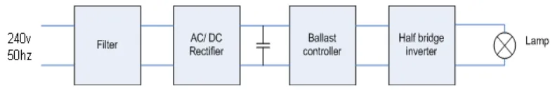
The output voltage of these four combination main parts is important because it is used by transformer, switching circuit and control circuit to switch ON the fluorescent lamp tube. The simple electronic ballast block diagram is as shown in Figure 1.1.
Figure 1.1: Electronic ballast block diagram.
The others important parts that has been discussed on this electronic ballast are harmonic filter and power factor correction circuit. It is important because these two parts used, to make sure the output of the current and voltage of this electronic ballast is under the harmonic and power factor standard rated value according to specified by Public Works Department. The standard value of the harmonic of the circuit is 25%. [3]
This project focuses on design the harmonic filter and power factor correction of the electronic ballast type RFO T8-36W 4 feet. This general electronic ballast is using a basic electronic ballast circuit as it mentions early. The electronic ballast circuit of this fluorescent lamp showed in figure 1.2 below.
This circuit needs to be improved by increase the power factor and reduce the current/voltage harmonic. To fulfill this improvement, the Valley-Fill Passive Power Factor Correction circuit in order to improve the power factor while reduced the voltage and current total harmonic distortion.
While there are a lot of technique can be use to increase the power factor and reduced the total harmonic distortion of the electronic ballast. By considering the cost value, valley-fill type suitable because these circuit quite easy and simple to design. This valley fill circuit are consists of 2 electrolytic capacitor and 3 diode. It is connected after full bridge controlled rectifier circuit. The valley-fill passive factor correction circuit is shown in figure 1.3.
Figure 1.3: Valley-Fill Passive Power Factor Correction Circuit.
1.2 Problem Statements
1.3 Project Objectives
This project focuses on the following two objectives:
1) Analysis and study the characteristic of the electronic ballast model RFO T8-36W based on design, operation, electrical characteristic such as current, power loss and voltage on transient and steady state.
2) To design and develop power factor correction and harmonics filter electronic ballast model RFO T8-36W.
1.4 Project Scopes
This project is covered the development of electronic ballast fluorescent lamp model RFO T8-36W. The project scope divided into 3 main parts:
1. Remodel the original and new design of electronic ballast fluorescent lamp model RFO T8-36W.
2. Test and measured both of the electronic ballast parameters based on power quality and harmonics.
3. Design the schematic both of the circuit by using OrCAD PSpice software simulation.
1.5 Literature Review
1) Main parts of electronic ballast 2) Fundamental
3) Simulation Software 4) Measurement equipments
5) Valley Fill Passive Power Factor Correction
1.6 Main Parts of Electronic Ballast
The existing of electronic ballast is use to replace the magnetic ballast conventional system. However, some of the electronic ballast still does not have the suitable electronic system which can use to increase the power factor and reduce the harmonic distortion. Electronic ballast divided into some parts which each part have there own function before turning-on the tube.
Each part needs to consider in term of input/output of current and voltage harmonic distortion. General electronic ballast has five mains component such as:
1) AC/DC rectifier 2) Capacitor Bank 3) Inverter
4) Filter
5) Ballast controller
1.6.1 AC/DC Rectifier
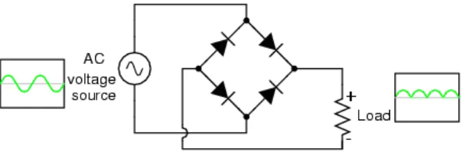
Commonly rectifiers are made by solid state diodes, vacuum tube diodes, mercury arc valves, and other components.
The efficiency of the converting AC to DC process can be increase by comprises a number of the diode but not in one diode. The most common diode used in the day time is vacuum tube diodes and copper (I) oxide or selenium rectifier. These types of rectifier are used before the development of silicon semiconductor rectifiers.
Crystal radios which used a "cat's whisker" of fine wire pressing on a crystal of galena (lead sulfide) to serve as a point-contact rectifier or "crystal detector" is develop early of the development of radio. In gas heating systems flame rectification can be used to detect a flame.
The flame is presented along the current path and rectification by two metal electrodes in the outer layer which is applied the alternating voltage [4]. The full bridge controlled rectifier show as figure 1.4 below.
Figure 1.4: Full Bridge Rectifier Circuit
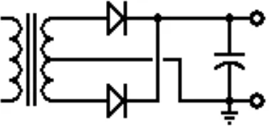
1.6.2 Capacitor Bank
Figure 1.5: Buffer Capacitor
When capacitor is placed at the output of the full-wave rectifier as shown to the left, the capacitor will charge to the peak voltage each half-cycle, and then will discharge more slowly through the load while the rectified voltage drops back to zero before beginning the next half-cycle. Thus, the capacitor helps to fill in the gaps between the peaks, as shown in red in the figure 1.7.
Although we have used straight lines for simplicity, the decay is actually the normal exponential decay of any capacitor discharging through a load resistor. The extent to which the capacitor voltage drops depends on the capacitance of the capacitor and the amount of current drawn by the load; these two factors effectively form the RC time constant for voltage decay.
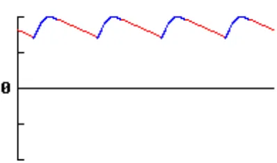
Figure 1.6: Input signal waveform
Figure 1.8: Filtered input signal waveform
The figure 1.8 shows the actual voltage output is never drop to zero condition. When the capacitor provides current to the load, its can show through the increase waveform which is provides current to the load and the decrease waveform show the capacitor provides current to the load.
At the unfiltered output of the rectifier not pure dc, has much less variation or called ripple. The capacitor will discharge considerably more between input pulses and at a half-wave the rectifier, the capacitor works as filter and filter the output voltage from the rectifier.
The capacitor filter many kid of loads if the output voltage from the can be kept high enough at all times [5].
1.6.3 Inverter
Inverter is an electronic component and it is used to converts the direct current to alternating current which is can be required voltage and frequency with the use of appropriate transformers, switching and control circuits. The inverter can be use at any kind of electrical and electronic system such as large electric utility high-voltage direct current applications that transport from small switching power in the computer.