Faculty of Electrical Engineering
COMPUTER VISION INSPECTION AND CLASSIFICATION ON
PRINTED CIRCUIT BOARDS FOR FLUX DEFECTS
Ang Teoh Ong
Doctor of Engineering
COMPUTER VISION INSPECTION AND CLASSIFICATION ON PRINTED CIRCUIT BOARDS FOR FLUX DEFECTS
ANG TEOH ONG
A thesis submitted
In fullfilment of the requirements for the degree of Doctor of Engineering
Faculty of Electrical Engineering
UNIVERSITI TEKNIKAL MALAYSIA MELAKA
DECLARATION
I hereby declare that the work in this thesis is my own research except as cited in the reference. The thesis has not been accepted for any degree and is not concurrently submitted in candidature of any other degree.
Signature : ………..
Name : ………..
APPROVAL
I hereby declare that I have read this thesis and in my opinion this thesis is sufficient in term of scope and quality for the award of Doctor of Engineering.
Signature : ………...
Supervisor Name : ………...
DEDICATION
ABSTRACT
The manual inspection of Printed Circuit Boards (PCB) is labor intensive and slow down the production line. During the assembly process, the defective PCBs with flux defects if not detected and remove, it can create corrosion and cause harmful effects on the board itself. As such, an automated inspection system is very much needed to overcome the aforementioned problems in PCB production line. The main objective of this work is to develop a real-time machine vision system for quality assessment of PCBs by detecting defectives PCBs. The proposed system should be able to detect flux defect on PCB board during the re-flow process and achieve good accuracy of the PCB quality checking. The proposed system is named as An Automatic Inspection System for Printed Circuit Boards (AIS-PCB), involves design and fabrication of a total automation control system involving the use of mechanical PCB loader/un-loader, robotic pneumatic system handler with vacuum cap and a vision inspection station that makes a decision either to accept or reject. The decision making part involves classifier training of PCB images. Prior to ANN training, the images need to be processed by the image processing and feature extraction. The image processing system is based on pattern matching and color image analysis techniques. The shape of the PCB pins is analyzed by using pattern matching technique to detect the PCB flux defect area. After that, the color analysis of the flux defect on a PCB boards are processed based on their red color pixel percentage in Red, Green and Blue (RGB) model. The red color filter band mean value of histogram is measured and compared to the value threshold to determine the occurrence of flux defect on the PCBs. The texture of the PCB flux defect can also be extracted based on line detection of the gradient field PCB images and feature indexing by using Radon transform-based approach. The feed-forward back-propagation (FFBP) model is used as classifier to classify the product quality of the PCBs via a learning concept. A number of trainings using the FFBP are performed for the classifier to learn and match the targets. The learned classifier, when tested on the PCBs from a factory’s production line, achieves a grading accuracy of coefficient of efficiency (COE) greater than 95%. As such, it can be concluded that the developed AIS-PCB system has shown promising results by successfully classifying flux defects in PCBs through visual information and facilitates automatic inspection, thereby aiding humans in conducting rapid inspections.
ABSTRAK
Pemeriksaan secara manual bagi Papan Litar Bercetak (PCB) memerlukan tenaga kerja yang intensif dan melambatkan aliran pengeluaran. Dalam proses pemasangan, PCB yang rosak jika tidak dikesan dan diasingkan, keadaan ini boleh menghasilkan kakisan dan menyebabkan kesan buruk terhadap PCB tersebut. Maka, pemeriksaan secara pemeriksaan penglihatan automatik yang sistematik adalah sangat diperlukan bagi mengatasi masalah yang dinyatakan di atas didalam aliran pengeluaran. Oleh itu, objektif utama kajian ini adalah untuk membangunkan satu sistem penglihatan mesin masa nyata untuk penilaian kualiti PCB dengan mengesan kecacatan pada flux PCB. Sistem yang dicadangkan didalam kajian ini akan berupaya mengesan kecacatan fluks pada papan PCB semasa proses aliran semula dan memperolehi ketepatan yang tinggi terhadap pemeriksaan kualiti PCB. Sistem yang dicadangkan, dinamakan sebagai Sistem Pemeriksaan Automatik bagi Papan Litar Bercetak (AIS-PCB), melibatkan reka bentuk dan fabrikasi sistem kawalan automasi yang melibatkan penggunaan PCB mekanikal 'loader'/'un-loader', pengendalian sistem pneumatik robotik dengan topi vakum dan stesen pemeriksaan penglihatan yang membuat keputusan sama ada diterima atau ditolak. Proses membuatan keputusan ialah melibatkan latihan pengkelasan imej PCB. Sebelum latihan, semua imej perlu melalui pemprosesan imej dan proses pengekstrakan ciri-ciri. Sistem pemprosesan imej adalah berdasarkan kepada corak yang hampir sama dan teknik analisis warna imej. Bentuk pin PCB dianalisia menggunakan teknik corak yang hampir sama untuk mengesan kawasan kecacatan fluks PCB. Selepas itu, teknik analisisa warna bagi kecacatan fluks papan PCB diproses berdasarkan peratusan piksel berwarna merah di dalam model Merah, Hijau dan Biru (RGB). Penuras warna merah bermaksud nilai histogram diukur dan dibandingkan dengan nilai ambang untuk menentukan sama ada berlakunya kecacatan fluks pada PCB. Tekstur kecacatan fluks PCB juga boleh diekstrak berdasarkan pengesanan garis medan kecerunan pada imej PCB dan ciri pengindeksan dengan menggunakan pendekatan terubah Radon. Model propagasi-belakang suapan-hadapan (FFBP) digunakan sebagai pengkelas untuk mengklasifikasikan kualiti PCB melalui konsep pembelajaran. Beberapa latihan menggunakan FFBP dilaksanakan bagi pengkelas untuk belajar dan memadankan dengan sasaran. Rangkaian pengelasan ini apabila diuji terhadap PCB dari aliran pengeluaran kilang telah didapati mencapai ketepatan pekali kecekapan (COE) melebihi 95%. Oleh itu, kesimpulan dapat dibuat bahawa sistem AIS-PCB yang dibangunkan ini telah memberikan keputusan yang memberangsangkan dengan keupayaan mengklasifikasikan kecacatan flux PCB melalui maklumat penglihatan dan memudahkan proses pemeriksaan secara automatik, dengan itu ia berupaya membantu manusia melaksanakan pemeriksaan secara pantas dan tepat.
ACKNOWLEDGEMENT
The author is pleased to express his deepest sense of gratitude and sencere devotion to his supervisor Prof. Dr. Zulkifilie Bin Ibrahim Mohd, Department of Electrical Engineering UTeM, for his continue supervision and helpful suggestion during the entire progress of this research.
The author wishes to thanks external supervisor PM. Dr. Suzaimah Ramli, UPNM for her help and encouragement during the reserach progress. The author wishes to extent the thanks to all member of the staff of Electrical Department , UTeM for their help and co-operation.
The author thanks all his friends and special thanks to Dr. Aoauche Mustapha and Prof. Dr. Aini, UKM for their support and guidance. Lastly, special appreciation to industry supervisor Mr. Boo Chai Eong, INTEL Penang especially for his advice and input from the industry aspects on this research.
TABLE OF CONTENTS
ACKNOWLEDGEMENTS iii
TABLE OF CONTENTS iv
1.3 Motivation for research 5
1.4 Problem statement 5
1.5 Objectives of research 8
1.6 Scope of research 9
1.7 Contribution of research 9
1.8 Organization of thesis 10
2. LITERATURE REVIEW 11
2.1 History of PCB technology 11
2.2 Literature review of PCB machine vision system 12
2.3 Automated grading system in PCB inspection 15
2.4 Summary 32
3. SYSTEM DESIGN 34
3.1 Introduction 34
3.2 Overview of proposed machine vision system 38
3.4 Data collection 48
3.4.1 Location 48
3.4.2 Equipment 48
3.4.3 Procedure 48
3.4.4 PCB (Printed Circuit Board) image samples 49
3.4.5 Consultation with factory 52
3.5 Flux defects inspection algorithms 53
3.5.1 Software tools 54
3.5.2 Proposed PCB inspection algorithms 54
3.5.3 Color analysis system 56 3.5.6 Color image processing using Matrox imaging library 69
3.5.6.1 Matrox MIL benefits 69
3.5.6.2 Pattern recognition using Matrox MIL 70
3.5.6.3 Color analysis 71
3.5.6.4 Fully optimized for speed 72
3.5.7 Color image processing using Matlab 73 3.5.7.1 Indexed images 75
3.5.9.1 Image processing algorithm 82
3.5.9.2 Segmentation 84
3.5.9.3 Thresholding 85
3.5.9.4 Fix threshold algorithm 86
3.5.9.5 Automatic threshold algorithm ( Otsu's Method ) 87
3.5.10 Feature extraction algorithms 90
3.5.11 Features extraction based on RGB color space 91 3.5.11.1 Techniques based on pattern matching 97
3.5.12.3 Radon Transform feature extraction and procedure 105
3.6 Design of Artificial Neural Network (ANN) classification 108
3.6.1 Simple neuron 110
3.6.2 Hard-limit transfer function 111
3.6.3 Linear transfer function 112
3.6.4 Sigmoid transfer function 112
4. RESULTS AND DISCUSSION 123
4.1 Introduction 123
4.2 Image Pre-Processing 123
4.3 Result of Otsu automatic threshold and fix threshold 124
4.3.1 Experimental Results 126
4.3.2 Fix and automatic threshold mean value 128 4.4 Otsu automatic threshold with RGB green, blue and
red-blue color filter 133 4.5 Otsu automatic threshold with RGB red color filter 137
4.5.1 Result 138
4.6 Automatic threshold with Radon Transform line detection 145 4.7 Testing and performance evaluation with ANN Classification 157
4.7.1 ANN neural network classification 157
4.7.2 Artificial neural networks performance evaluation 160
4.7.3 Training stage result 161
4.7.4 Testing stage result 163
4.8 Comparative study of Human manual inspection, RGB and Radon
Transform line detection 164
4.8.1 Result comparison 164
4.8.2 Software and tool validation 166
4.9 Economical impact 166
5.2 Attainment of research objectives 174
5.3 Significant contribution of research output 175
5.4 Suggestion for future work 175
REFERENCE 176
APPENDICES 186
LIST OF TABLES
TABLE TITLE PAGE
1.1
2.1 PCB inspection problem statements Types of defects 5 14
3.1 Data for input / output port 47
3.2 RGB color space parameters 67
3.3 The ROI (MExR RED-Band) of the sample images with mean
value 101
3.4 Statistical criteria for the evaluation of the models in the training
stage 120
4.1 (a) Fix threshold mean value 128
4.1 (b) Automatic threshold mean value 129
4.2 (a) Average mean value between fix threshold and automatic
threshold 130
4.2 (b) Average mean value between fix threshold and automatic
threshold 130
4.3 Images and red color filter band mean value 138
4.4 Statistical measure from ANN-models (training stage) for different learning algorithms simulation between measured and examined
161
4.5 Statistical measure from ANN-models (testing stage) for best
learning algorithms simulation between measured and examined 164
4.6 Operation cost before AOI implementation 170
4.7 Operation cost after AOI implementation 171
4.8 Cost comparison between human manual inspection and AOI 172
LIST OF FIGURES
FIGURE TITLE PAGE
1.1 1.2
1.3
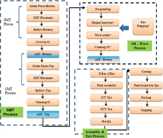
PCBA general process flow chart
Flux residue surrounding solder joints of BGA FET and on the baord
Flux residue under 1210 chip capacitors
2 6 7
3.1(a) Machine vision configuration set-up 35
3.1(b) Inspection system block diagram 35
3.2 Basic machine vision PCB image grading processing flow chart 37
3.3 Components of the image processing system 39
3.4 Proposed PCB inspection system 41
3.5 Advantech 4711A USB DAQ Port Configuration 44
3.6
3.7 DAQ output LED interface port Overview of the proposed PCB automatic inspection set-up 46 49
3.8 PCB with flux data base samples class 50
3.9 PCB without flux data base samples class 51
3.10 Data collection flow 52
3.11 HSV color model 58
3.12 HSV time-varied cone 59
3.13 HSV time-varied cylinder 60
3.14 RGB color model 64
3.15 HSV-RGB comparison 68
3.16 Barns grand tetons HSV separation 68
3.17 Matrox vision PCB flux images processing preview 70
3.18 Matrox MIL Pattern Matching function 71
3.19 Matrox MIL color analysis function 72
3.20 Sample of Matlab vision PCB flux images processing preview 79
3.21 Flow chart of Image pre-processing 80
3.22 PCB flux image processing algorithms block diagram (a) based on MExR red color filter and (b) based on radon transform line detection algorithm
82
3.23 Filtering the primaries color separately 84
3.24 Example of Thresholding the PCB image 85
3.25 Image processing with fix threshold algorithms block diagram 87 3.26 PCB segmentation and automatic threshold algorithm 88 3.27 Image processing algorithms with automatic threshold
algorithm 88
3.28
3.29 Optimal or adaptive thresholding Binary images threshold 89 93 3.30(a) PCB binary image (with flux defect) and rotated angle 93
3.30(b) Finding the rotated PCB image angle 94 3.31 The ROI on the reference image where pattern matching search
model for 3 IC’s pin 95
3.32 Flow chart of Proposed image processing algorithm 96 3.33 (1) Extracted Image (MExR Red-Band), (2) T = 170, (3) T =80,
(4) T = 10 100
3.34 Histogram for ROI (MExR RED-Band) of PCB flux image 101
3.35 An image and its histogram 103
3.36 Illustration of (a) step 1 and step 2 (b) determination of the
maximum and minimum value/s of either x or y (step 3) 106
3.37 Selection of angle (step 4) 107
3.38 Neural Network image index feature concept 110
3.39 Simple Neuron 110
3.40 Hard-limit Transfer Function 111
3.41 Linear Transfer Function 112
3.42 Sigmoid Transfer Function 112
3.43 Neuron with vector input 113
3.44 Input vector p 114
3.45 Feed Forward Neural Network 116
3.46 Two-layer tansig/purelin Network 117
3.47 Architecture for ANN topology 117
4.1 After resize, the image has become 150x150 pixels 127
4.2 Threshold the image using Otsu rules 127
4.3 Threshold the image using Fix Threshold 10 127
4.4 Threshold the image using Fix Threshold 80 127
4.5 Threshold the image using Fix Threshold 170 127
4.6 Threshold image with fix threshold and automatic threshold for
PCB with flux category 131
4.7 Threshold image with fix threshold and automatic threshold for
PCB without flux category 132
4.8 Result of Otsu automatic threshold with RGB green color filter 134 4.9 Result of Otsu automatic threshold with RGB blue color filter 135 4.10 Result of Otsu automatic threshold with RGB red-blue color
filter 136
4.11 Red color flux and Histogram with automatic threshold for
PCB with flux category 144
4.12 After resize, the image has become 150x150 pixels 146
4.13 First and second subtraction 146
4.14 Mask and morphological operation 146
4.15 Final segmentation image 147
4.16 Result of the flux defect segmentation 152
4.17 Results of the PCB flux defect feature extraction 156 4.18 Radon transform automatic threshold training errors 159 4.19 Radon transform automatic threshold before training 159 4.20 Radon transform automatic threshold after training 160 4.21 ANN classification performance in the training stage 162 4.22 ANN classification performance in the testing stage 163 4.23 Comparison result of Human manual inspection, RGB and
radon transform line detection 165
4.24 Software and tool validation 166
LIST OF APPENDICES
APPENDIX TITLE PAGE
A1 A2 A3 A4 A5
Machine vision conceptual mechanical drawing
SAMSUNG CCD Camera, Matrox Frame grabber and Matrox 4-sight GPm Industrial imaging computer
Automation components source code Matrox programming source code Matlab programming source code
186 191 203 208 233
LIST OF ABBREVIATIONS
AF Auto Focus
AIS Automatic Inspection System ANN Artificial Neural Network AOI Automatic Optical Inspection API Application Program Interface
ASIC Application-Specific Integrated Circuit
AUC Area Under The Curve
AVI Automated visual inspection BIOS
BGA FET Basic Input/output System Ball Grid Array Field-effect Transistor
BNC Bayonet Neill-Concelman
BW Black And White
CAGR Compound Annual Growth Rate
CB Clear Image Border
CCD Charge-Coupled Device
CCIR Consultative Committee For International Radio COE Coefficient of Efficiency
CMM Coordinate Measuring Machine
CMYK Cyan, Magenta, Yellow, Key
CPU Central Processing Unit
CRT Cathode Ray Tube
CVBS Composite Video Baseband Signal
DAQ Data Acquisition
DIO Digital I/O
ED Edge Image
ELCB Earth Leakage Circuit Breaker
FCT Functional Testing
FDS Flux Defect Segmentation
FFBP Feed-Forward Back -Propagation
FN False Negative
FP False Positive
FPGA Field-Programmable Gate Array
FS First Subtraction
GA Genetic Algorithm
GLPF Gaussian Low-Pass Filter GUI Graphical User Interface
HPC High-Performance Computing
HSB Hue, Saturation, Brightness HSL Hue, Saturation, Lightness
HSV Hue-Saturation-Value
I/O Input/output
IC Integrated Circuit
ICT In-Circuit Test
LED Light-Emitting Diode
LM Levenberg-Marquardt
LPT Line Print Terminal
LUT Look-Up Table
MAE Mean Absolute Error
MCB Miniature Circuit Breakers
MExG Modified Excess Green
MExR Modified Excess Red
MI Manual Insert
MIL Matrox Imaging Library
MLP Multi-Layer Perceptron
MO Morphological Opening
NGC Normalized Gray Scale Correlation NTSC National Television System Committee OCR Optical Character Recognition
PAL Phase Alternative Line
PC Personal Computer
PCB Printed Circuit Board
PCBA Printed Circuit Board Assembly PCI Protocol Control Information
QA Quality Assurance
RBF Radial Basis Function
RCA Radio Corporation Of America
RGB Red, Green, Blue
RMSE Root Mean Square Error
ROC Receiver Operating Characteristic
ROI Region Of Interest
RT Radon Transform
SATA Serial ATA
SCG Scaled Conjugate Gradient
SIMD Single Instruction Multiple Data
SMT Surface Mount Technology
SS Second Subtraction
SSEx Streaming SIMD Extensions
LIST OF SYMBOLS
bpp - Bits per pixel
D - Dimension
GB - Gigabyte
GHz - Gigahertz
hex - Hexadecimal
m - Meter
MB - Megabyte
MHz - Megahertz
rpm - Revolution per minute
TB - Terabyte
V - Volt
LIST OF PUBLICATIONS
Ang Teoh Ong, Zulkifilie Bin Ibrahim, Suzaimah Ramli (2013). Computer Machine Vision Inspection on Printed Circuit Boards Flux Defects, American Journal of Engineering and Applied Sciences 6(3): 263-273, 2013.
Ang Teoh Ong, Aouache Mustapha, Zulkifilie Bin Ibrahim, Suzaimah Ramli, Boo Chai Eong (2015). Real-Time Automatic Inspection System for the classification of PCB Flux Defects. American Journal of Engineering and Applied Sciences, 2015.
THE 6th International Conference on Postgraduate Education
Image Processing Based Method For Printed Circuit Boards Flux Defects Detection. Main Hall UTeM, Melaka, 17 - 18 December 2014.
1 CHAPTER 1
INTRODUCTION
1.1 Background
PC-Based vision technology has been developed and utilized as a part of a wide range of industry territory applications. One of the vision inspection applications is machine vision inspection on detect of the printed circuit board (PCB). Machine vision inspection is critical because it evacuates the deformities subjective elements and gives quantitative, quick and dimensional evaluations. PCBs typically contain complicated and definite format pattern designs; with this reason manual visual inspection is extremely exhausting and can caused many human errors. On the other hand, automatic machine vision systems are very consistent, accurate, fast and do not get exhausted.
2
Remark: * Depend on the board design functionality. Figure 1.1 below show the PCBA (Printed Circuit Board Assembly) general process flow chart in PCB industry manufacturing sector. The process involved SMT process for bottom and top level, MI (Manual Insert) process and finally assembly and test process. This research main focus is machine vision inspection algorithm technique on PCB flux defects, which has been applied in process AOI - Bottom, AOI - Top and Manual Insert AOI - Bottom.
3
Initially, PCB’s artwork generation was a full-time manual process performed on clear Mylar sheets at a scale of generally 2 or 4 times the desired size. Modern practice comprises computers that handle almost every task automatically and less labor intensive. Pattern-matching method is the most commonly image processing technique used in the machine vision application. Due to the rapid development in computer technology, this method became practicable and affordable. In addition, frame grabber was used to transmit the images from camera to computer and follow by image processing analysis.
The manual inspection of PCB defects might cause labor intensive and subjects to human error and inconsistent grading which can be solved by automatic inspection process with “Computer Machine Vision Inspection”. This system applies a connectivity approach to detect the fatal defects such as PCB board printing and labelling, circuit bridging and scratches. Furthermore, this system is able to identify the marking of the components, components orientation, missing components, and so on.
4 1.2 Computer Vision System
Computer technology is in progress and becoming more powerful, computer vision equipment is presently moderately economical. Computer vision system basically requires a camera, a frame grabber and a computer. Now days, a basic computer vision system can be supported with personal computers which including a camera and others interface components. Never the less, there are also high performance computer vision system which can be very costly.
Automatic visual inspection of PCB boards is developed by using computer vision techniques to evaluate the performance and various PCB board defects. The fault detection strategy is very critical in this design and it is based on referential inspection method where the board artwork or a manufactured board without errors is chosen as a benchmark. The PCB defects can be classified into two main categories, the fatal defects (reject units) and no defects (accept units). This system is very effective to detect the fatal defects by subtracting the reference board image from the tested board image using image comparison technique and subsequently separates the good and defect boards.
5 1.3 Motivation for Research
The motivation for this research is to overcome the problems at the existing inspection on PCB flux defects, which was done in manual system by operator. This manual inspection is slow and brings more mistakes due to human error. Automatic computer vision inspection makes the inspection process faster and more consistent than manual inspection. In addition, the cost will be reduced significantly in long run with the return of investment less than two years period. Since the percentage of PCB flux defects is high, there subsists a prospect of introducing and implementing a computerized PCB inspection system to remove the subjective aspects rather than manual inspection. At the same time, the automated PCB examination system provides real time assessment of the PCB quality inspection.
1.4 Problem Statement
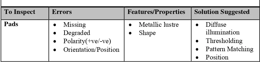
The main disadvantage of manual inspection of PCB defects are human mistakes, labour intensive and inconsistent result in evaluating. Problem statement might be varied depending on the inspection components and their respective features. In this case the inspection is carried out after all the PCB components have soldered. The problem statement together with error, components feature and solution applied is summarise in the table below.
Table 1.1:PCB inspection problem statements
PCB Inspection Problem Statement Summary
To Inspect Errors Features/Properties Solution Suggested Pads Missing
Degraded
Polarity(+ve/-ve) Orientation/Position
Metallic lustre