DESIGN OF INTEGRATED LOW-NOISE AMPLIFIER AND FILTER FOR WIRELESS COMMUNICATION APPLICATION
QUEE YU LEONG
DESIGN OF INTEGRATED LOW-NOISE AMPLIFIER AND FILTER FOR WIRELESS COMMUNICATION APPLICATION
QUEE YU LEONG
This report submitted in partial fulfillment of the requirements for the award of Bachelor of Electronic Engineering (Telecommunications Electronics) With
Honours
Faculty of Electronics and Computer Engineering Universiti Teknikal Malaysia Melaka
v
DEDICATION
This thesis is dedicated to my beloved parents,
Quee Lin Sai & Chiow Boon Ching
To my supervisor,
PM. Dr. Zahriladha Bin Zakaria
My friends and my fellow lecturers
vi
ACKNOWLEDGMENT
vii
ABSTRACT
viii
ABSTRAK
ix
TABLE OF CONTENTS
CHAPTER CONTENT PAGES
TITLE i
REPORT STATUS VERIFICATION FORM ii
DECLARATION iii
APPROVAL iv
DEDICATION v
ACKNOWLEDGMENT vi
ABSTRACT vii
ABSTRAK viii
TABLE OF CONTENTS ix
LIST OF FIGURES xii
LIST OF TABLES xiv
LIST OF ABBREVIATIONS xv
LIST OF APPENDICES xvi
I INTRODUCTIONS
1.1 INTRODUCTION 1
1.2 PROJECT OBJECTIVES 4
1.3 PROBLEM STATEMENT 4
1.4 SCOPE OF WORK 5
x
II LITERATURE REVIEW
2.1 FREQUENCY BANDS OF 1.7-2.7 GHz 7
2.1.1 ISM BAND 7
2.1.2 GSM CELLULAR BAND 8
2.2 INTRODUCTION OF LOW-NOISE AMPLIFIER 9
2.3 TWO-PORT NETWORK 9
2.4NOISE FIGURE 10
2.5 S-PARAMETER 12
2.6 STABILITY 13
2.7 TWO-PORT POWER GAIN 13
2.8 JUNCTION FIELD EFFECT TRANSISTOR BIASING 14
2.9INPUT AND OUTPUT MATCHING 16
2.9.1 QUARTER-WAVE TRANSFORMER MATCHING 17
2.10NOTCH FILTER 18
2.11 RELATED RESEARCH 19
III METHODOLOGY
3.1 PROJECT METHODOLOGY 22
3.2 DESIGNING LOW-NOISE AMPLIFIER 25
3.2.1TRANSISTOR SELECTION 25
3.2.2 STABILITY ANALYSIS 26
3.2.3 BIAS POINT SELECTION 27
3.2.4 DESIGNING BIAS NETWORK 27
3.2.5 INPUT AND OUTPUT MATCHING 28
3.3 DESIGNING NOTCH FILTER 28
3.4 INTEGRATED OF LOW-NOISE AMPLIFIER 28
xi
IV RESULT AND ANALYSIS
4.1 STABILITY ANALYSIS 29
4.2 BIAS POINT SELECTION 32
4.3 TWO-PORT POWER GAIN 33
4.4 BIASING NETWORK DESIGN 35
4.5 INPUT AND OUTPUT MATCHING NETWORK 37
4.5.1 QUARTER-WAVE TRANSFORMER MATCHING 40
4.5.2 DESIGN WITH IDEAL COMPONENTS 42
4.5.3 DESIGN WITH NON-IDEAL COMPONENTS 45
4.6 DESIGN OF NOTCH FILTER 48
4.7 INTEGRATED OF LOW-NOISE AMPLIFIER 50
AND NOTCH FILTER
V CONCLUSION AND FUTURE WORKS
5.1 CONCLUSION 54
5.2 FUTURE WORK 55
REFERENCE 56
xii
LIST OF FIGURE
Figure 1.1: Basis Block Diagram of RF Receiver 2
Figure 1.2: The Characteristic of Notch Filter 3
Figure 2.1: Two-Port Network 10
Figure 2.2: Electrical Network of S-Parameters 12
Figure 2.3: Circuit of Self-Bias 15
Figure 2.4: Circuit of Voltage Divider Bias 15
Figure 2.5: Lossless Network Matching 16
Figure 2.6: Quarter-Wave TransformerMatching 18
Figure 2.7: Equivalent Circuits of Bandstop Filters with 18 Shunt Series-Resonant Branches
Figure 2.8: Equivalent Circuits of Bandstop Filters with 18 Series Parallel-Resonant Branches
Figure 3.1: Flow Chart for Methodology 23
Figure 4.1: Schematic for Stability Test 30
Figure 4.2: Simulation Result of Transistor Stability Test 30 Figure 4.3: Stability Test with Negative Feedback 31 Figure 4.4: Simulation Result of Stability Test with Negative Feedback 31 Figure 4.5: I-V Characteristics Simulation Setup in ADS 32
Figure 4.6: I-V Curves of Transistor ATF-54143 32
xiii
Figure 4.8: Biasing Network 36
Figure 4.9:Circuit of Unmatched LNA Design 38
Figure 4.10: Simulation Result of S11 & S22 for Unmatched LNA Design 38
Figure 4.11: Simulation Result of S21 & S12 for Unmatched LNA Design 39 Figure 4.12: Simulation Result of Noise Figure for Unmatched LNA Design 39 Figure 4.13: Impedance of Matching Circuit for Gain and Noise Figure 40 Figure 4.14: Quarter-Wave Transformer Input Matching Circuit 41 Figure 4.15: Quarter-Wave Transformer Output Matching Circuit 42 Figure 4.16: Schematic of LNA with Ideal Quarter-Wave Transformer Matching 43 Figure 4.17: Simulation Result of Return Loss by Ideal Matching Components 43 Figure 4.18: Simulation Result of Noise Figure by Ideal Matching Components 44 Figure 4.19: Simulation Result of Gain by Ideal Matching Components 44 Figure 4.20: Schematic of LNA with Non-Ideal Quarter-Wave Transformer 46
Matching
Figure 4.21: Simulation Result of Noise Figure by Non-Ideal 46 Matching Components
Figure 4.22: Simulation Result of Return Loss by Non-Ideal 47 Matching Components
Figure 4.23: Simulation Result of Gain by Non-Ideal Matching Components 47
Figure 4.24: Notch filter with Lumped Element 49
Figure 4.25: Simulation Result of Notch Filter 50
Figure 4.26: Schematic of Integrated of LNA and Notch Filter 51 Figure 4.27: Simulation Result of Noise figure (NF) for Integrated of 51
LNA and Notch Filter
Figure 4.28: Simulation Result of Gain for Integrated LNA and Notch Filter 52 Figure 4.29: Simulation Result of Return Loss for Integrated 52
xiv
LIST OF TABLES
Table 2.1: Allocations of GSM Band 8
Table 2.2: Types of Biasing Circuit and Formula 15
Table 2.3: Review on Low-Noise Amplifier 21
xv
LIST OF ABBREVIATIONS
LNA - Low-Noise Amplifier
GPS - Global Positioning System
WLAN - Wireless Local Area Network
WiMAX - Worldwide Interoperability for Microwave Access
BW - Bandwidth
SNR - Signal-to-Noise Ratio
LO - Local-Oscillator
DSP - Digital Signal Processing
PCS - Personal Communications Services
ADC - Analog-to-Digital Converter
WLL - Wireless Local Loop
RLL - Run Length Limited
MMDS - Multichannel Multipoint Distribution Service
ADS - Advance Design System
RF - Radio Frequency
NF - Noise Figure
CMOS - Complementary Metal–Oxide–Semiconductor
EM - Electromagnetic
ISM - Industrial, Scientific and Medical
GSM - Global System for Mobile Communications
TDMA - Time Division Multiple Access
xvi
LIST OF APPENDICES
APPENDIX TITLE PAGES
A Transistor Datasheet (ATF-54143) 59
B Smith Chart of Input Matching 75
1
CHAPTER I
INTRODUCTION
This chapter is about an introduction of project which includes an explanation of the project background, a brief introduction of wideband low-noise amplifier (LNA) and notch filter, method used in LNA design, objectives of a project, problem statement of the project, and the project scopes.
1.1 Introduction
Today, wireless communication technology is growing tremendously due to higher demand for high speed data communication. Cellular telephones, wireless local area networks (WLAN), global positioning system (GPS), and short-range data communication devices employing Bluetooth technologies are examples of portable wireless communication application [1]. Referable to the vast and insatiable need for affordable and low-power multi-standard portable devices, RF designers are urged to build up novel methodologies that take into account the invention of such products [1].
2
might be really faint and can’t be retrieved. Therefore, the LNA is used to amplify the low power signal received by antenna to an accepted and useful level. An LNA is good as it adds little noise as possible in itself and has high gain.
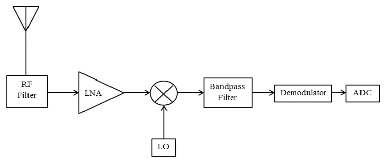
The basis block diagram of RF receiver structure is presented as Figure 1.1. Before amplified by an LNA, the signal received by antenna is normally filtered by RF filter first and then unite with a local-oscillator (LO) to metamorphose to the base-band. After demodulated process, the signal is processed to an analog-to-digital converter (ADC) which translates the analog signal into a digital signal. Then, the digital signal is utilized in a digital signal processing unit (DSP). The primary step of signal amplification is complete by the LNA. Therefore, the properties of LNA can easily affect the overall noise and sensitivity parameter of the entire receiver [1].
Figure 1.1: Basis Block Diagram of RF Receiver.
3
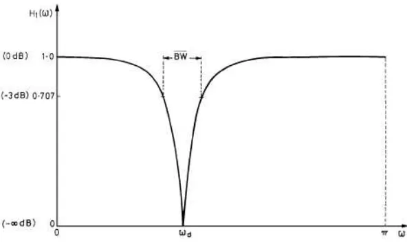
Figure 1.2: The Characteristic of Notch Filter.
4
1.2 Project Objectives
Wideband Low-noise amplifier (LNA) is an integrated component of most RF front end receiver systems. The main objectives of the thesis work are followed:
1. To study the background of LNA design and Notch filter.
2. To design an LNA and integrate with notch filter in order to minimize the undesired interferences from other frequency bands.
3. To analyze the performance of the LNA and LNA incorporated with notch filter based on electromagnetic (EM) simulations to determine return loss, notch response, stability, noise figure and gain.
1.3 Problem Statement
In general, a portable radio device such as mobile phone may include more than one radio operating in a cellular band, and a radio operating in the ISM band. The wideband low noise amplifier which covers 1.7-2.7 GHz range includes wireless LAN 802.11b, ISM band and cellular band. This environment presents a challenge since these radios may be in close physical proximity and located in the same physical instance. A high power interference such as cellular phone in the 1.9GHz frequency band may cause the ISM band receivers operating at 2.4 GHz to saturate since it is in close proximity to the 2.4 G Hz signal. This noise may cause a damaging consequence on the received wideband signal [3].
5
Some existing solutions may incorporate an on-board notch filter in the ISM band radio. This notch filter may be located between a low noise amplifier (LNA) and the mixer in the RF portion of the ISM band radio. This is to minimize the undesired interferences from other frequency bands [3].
1.4 Scope of Work
For this project, the scope is to design Integrated Low-Noise Amplifier and Notch Filter for wireless communication application which covers the frequency range of 1.7 GHz – 2.7 GHz. It can be split into five parts which are:
i. To study on how to design an integrated Low-Noise Amplifier and Notch Filter which covers the frequency range of 1.7 GHz – 2.7 GHz and can support wireless communication application.
ii. In design working process consists of three main parts which is simulation, testing, analysis and optimization.
iii. The S-parameter that is involved in the design such as noise figure, gain, return loss and notch response is analyzed.
6
1.5 Chapter Review
Chapter 1 is about an introduction of project which includes an explanation of the project background, a brief introduction of the wideband low noise amplifier (LNA) and notch filter, objectives of a project, problem statement, and the project scopes.
Chapter 2 is about the background study define in details for integrated low noise amplifier and notch filter. The literature review of the low noise amplifier, especially on the parameters and the design techniques used in the design procedure to also define in detail.
Chapter 3 contains research methodologies which include the step to design the integrated low noise amplifier and notch filter. This chapter also includes detailed explanations of a low noise amplifier and notch filter design technique and calculation that involved.
Chapter 4 is discussing about the results and analysis the simulation of integrated low noise amplifier and notch filter from stability consideration until the implementation of the LNA and notch filter.
7
CHAPTER II
LITERATURE REVIEW
This chapter defines about the background study define in details for integrated of a low noise amplifier and notch filter. The literature review of the low noise amplifier, especially on the parameters and the design techniques used in the design procedure to also set in detail.
2.1Frequency Bands of 1.7 to 2.7 GHz
There are several frequency bands including in the 1.7 to 2.7 GHz frequency range, which is ISM band, GSM cellular bands and others.
2.1.1 ISM Band