A Development of Class E Converter Circuit for Loosely Coupled
Inductive Power Transfer System
NOREZMI JAMAL, SHAKIR SAAT and Y. YUSMARNITA Faculty of Electronics and Computer Engineering Universiti Teknikal Malaysia Melaka, 76100 Durian Tunggal
MALAYSIA [email protected]
Abstract: - This paper presents an Inductive Power Transfer (IPT) system design using a Class E converter circuit. The Class E converter is used to drive a nonlinear load and theoretically it offers 100% efficiency. To be specifically, the performance of IPT system at 1MHz operating frequency and 9V DC supply voltage is analyzed. Voltage doubler rectifier and Darlington circuit are proposed in this paper to maximize output power. Moreover, to ensure the resonant inductive coupling in IPT system,capacitor compensation is also proposed in this work. Based on the experimental results, the output power with the capacitor compensation circuit is 1.6W at 15 mm air gap distance is better than the circuit without a capacitor compensation.
Key-Words: - IPT system, Class E converter circuit, Voltage doubler and Darlington circuit.
1 Introduction
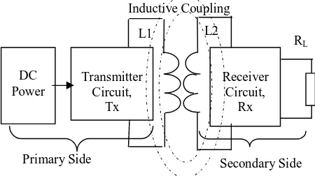
Inductive Power Transfer (IPT) is a recent wireless power transfer technology, which employ magnetic field in transferring the power without a wire contact at near field . To be specific, the IPT system consists of two coils which are separated by an air gap. First coil, L1 is connected to the transmitter circuit; while the second coil, L2 is connected to the receiver circuit, (see Fig. 1). The linked of two coils with the coupling coefficient is less than one can be known as a loosely coupled IPT [1].
Fig. 1.General Block Diagram of IPT System
Since the inductive is coupled through an air gap, so the leakage flux will occur during the transmission of power [ 1]. As a result, there is some power losses are expected to happen. Due to this problem, there are various methods available to ensure the maximum power transfer between transmitter and receiver circuit can be obtained. In
[2], authors summarized that there are three methods of power flow control in IPT systems, which are 1) primary power supply control at transmitter circuit, 2) secondary power pick up control at receiver circuit, and 3) dual control for both sides circuit. The results of that paper confirmed that dual control offers a number of advantages compare to others method. Therefore, the dual control will be considered in this paper.
A Class E converter circuit has been proposed in our work to increase the efficiency of the power transfer. This is because the Class E converter circuit guarantees that the switching loss is always at a very minimum level [3, 4]. Meanwhile, the capacitor compensation circuit needs to be connected either in series or parallel in order to achieve resonant inductive coupling [5]. This technique will ensure the maximum power transfer to the load. Then, voltage doubler and Darlington circuit is proposed to increase the current and also the voltage at the receiver circuit. Therefore, through the proposed approach, this paper aims to investigate the performance of IPT system at 1MHz using Class E converter and 9V DC supply that is able to power-up the low-power electronic devices.
2 General IPT System
Normally, there are four important elements in IPT system; 1) primary supply, 2) inductive coupling, 3) capacitor compensation, and 4) secondary pickup circuit. The detail discussion of these elements will be given in the following section.
Primary Side
L2 L1
Inductive Coupling
Transmitter Circuit,
Tx
Receiver Circuit,
Rx DC
Power
RL
2.1 Primary Supply
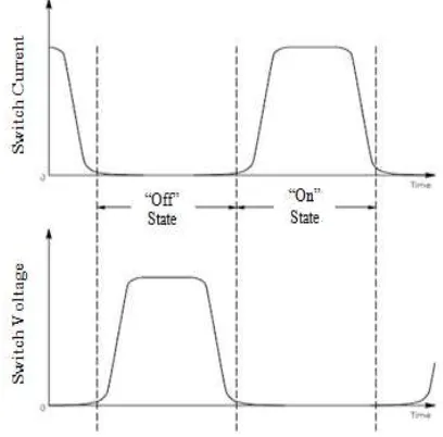
Class E converter circuit is a most suitable power converter to drive a non-linear load in the primary supply. Its operation is based on the Zero Voltage Switching (ZVS) concept. ZVS is a soft switching method where the turn-on transition of transistor occurs at every instant of zero voltage triggered [6]. Therefore, the current and voltage waveforms of switching are not overlap to each other, (see Fig. 2). This is to ensure the switching losses of this type of converter is low and therefore could increase the efficiency of overall circuit [6].
Fig. 2. Theoretical Current and Voltage Waveform during Class E converter Switching
The general Class E converter circuit is shown in Fig. 3. It consists of a single switch like a MOSFET. For the n-channel MOSFET, it will be triggered when receives the positive pulse. So, it is easy to be controlled.
Fig. 3. Class E Converter Circuit Schematic
2.2 Inductive Coupling
In inductive coupling, two winding coils (L1 and L2) are used to couple or link together as shown in Fig. 4. The power is transmitted by utilizing the changing of magnetic field when induced the voltage from the first coil onto second coil. The induced voltage at inductive coupling is only due to the alternating current, AC from a transmitter circuit.
Fig. 4. Inductive Coupling
Due to this behavior, the dependent voltage sources, V12 exists at primary side and it is induced
by I2 . The V12 can be found as follows where the
internal resistances (R1 and R2)are neglected as [1]
Then, the dependent voltage sources, V21 which is
induced by I1 can be written as
21 1
.
V j MI (14)
Meanwhile, the mutual inductance coupling can be regarded to their self inductance by coupling coefficient, k as follows:
1 2
;
M k
L L
(15)
where, M is the mutual inductance between primary coil, L1 and secondary coil, L2.
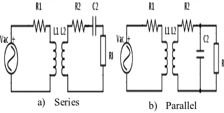
2.3 Capacitor Compensation
Since the loosely coupled IPT system is coupled between the first coil and the secondary coils through an air gap, therefore the coupling is weak. In order to enhance the power transfer performance, therefore, a capacitor is required to be connected at the secondary coil either in series or parallel connection [7]. In case of secondary series compensation, the resonance only occurs when the voltage across the inductive coil and capacitve compensation cancel each other. Then, it will act as
12 2
.
V j MI (13)
V I2 V12
M
I1
V21
Cshunt
Cseries Lseries
Lchoke
a voltage source which can supply the constant voltage source to the load. While in the case of secondary parallel compensation, the resonance only occur when the current through the secondary inductive coil cancel out with the parallel capacitor compensation and acts as a current source to supply a constant current to the load [8]. Fig. 5 shows two basic topologies for secondary compensation at receiver circuit.
a) Series b) Parallel Fig. 5. Secondary Capacitor Compensation
To simplify the circuit analysis, the existence of R1 and R2 can be neglected because their values are
very much smaller than the load resistance. The secondary compensation capacitor, C2 is designed
consciously to achieve the resonance with the secondary coil, L2 at operating frequency, fo as
follows:
2 2
1 2 o
f
L C
(16)
2.4 Secondary Pickup Circuit
During the power transmission from the transmitter circuit to the receiver circuit, there is a flux leakage. Hence, when the transmission distance is longer, then, the output power level is lower. Thus, a voltage doubler is proposed to be used in our developed IPT system. This circuit is required at the secondary circuit to rectify the AC power into DC power, and at the same time produces higher output voltage which is two times greater than the applied input voltage. Furthermore, the darlington circuit is proposed in our work to increase the current in this IPT system. This significantly leads to a higher power receive at the load.
3 IPT System Design
Based on the Fig. 6, IRF510 MOSFET is used as a switching device in the Class E converter to achieve the ZVS condition. This type of MOSFET is preferred due to low on-resistance, low cost and suitable for fast switching. Then, the values of
passive elements for Class E converter circuit are determined based on the an exact analysis technique [9]. Load resistance, RL= 0.5514(VDD) 2/Po. Next, the
value of shunt capacitor can be determined as Cshunt
= 0.1971/(ωRL) [10] while the series capacitor,
Cseries = 0.1062/(ωRL) [10] with 9V DC supply and
1MHz operating frequency. If the operating frequency is greater than the resonant frequency, resonant series circuit represents an inductive load at the operating frequency, f. Therefore, the inductance, Lseries can be divided into two
inductances, Lext and Lres, connected in series such
that L1= Lext + Lres and Lres where Lext= 1.153RL/ω
and Lres = 10.62RL/ω[10]. RF Choke Inductor, Lchoke
is chosen to be high enough so that can neglect an ac ripple [6].
To achieve better efficiency of power transfer between two coils, authors in [11] stated that the single layer coil is better to be used than the multi layer coil. So, in this work, the single layer coil is used. The size of wireless coil devices are 37.0 mm x 37.0 mm x 1.8 mm for 10µH. The coils are attached on the ferrite core as to shield the magnetic flux as well as to increase the coupling coefficient of the inductive which then improves the contactless power transfer [12]. On the other hand, voltage doubler and Darlington circuit are proposed to be used in the system to achieve high current and high voltage since there is a current leakage during the power transfer through an air gap. In the voltage doubler circuit, two 1N4148 diodes are used with two 10nF ceramic capacitor for rectification purpose and at the same time increase the voltage. Higher frequency will cause the low value of selected ceramic capacitor. Theoretically, the DC output voltage of multiplier circuit will increase twice from an AC voltage. The capacitor is connected on parallel after the rectification to filter the AC
Voltage Doubler
Class E Converter
Darlington Circuit
variations. Next, two NPN (BC547) transistors are used to amplify the current, which based on the current gain. A resistor, R1 is connected to the base of the Darlington to act as a protection circuit. Table I shows the Class E converter circuit specifications. In this paper, the Class E converter circuit is designed with 9V DC supply, VDD , 50% optimal of
the switch duty cycle, D, 3W maximum output power, Po , 1MHz operating frequency, f and quality
factor, Q of a series resonant circuit is 10.
Table I Class E Converter Circuit Specifications
Parameters Simulated Measured
Quality Factor, Q 10.0 10.0 Choke Inductor, Lchoke 5.0mH 5.0mH
Shunt Capacitor, Cshunt 2.1nF 2.2nF
Series Capacitor, Cseries 1.1nF 1.0nF
Series Inductance, Lseries 19.7µH 22.0µH
Primary and Secondary Coil, L1 and L2
10µH 10µH
Internal Primary Resistance Coil, R1
- 0.3Ω
Internal Secondary Resistance Coil, R2
- 0.2Ω
4 Results and Discussion
This section consists of simulation and experimental results. The class E converter circuit simulations are obtained first to determine the ZVS of the power converter. Then, experimental results are delivered to confirm the theoretical and simulation results. The performance of the IPT system with compensation and without compensation are discussed in this section too.
4.1 Simulation Results
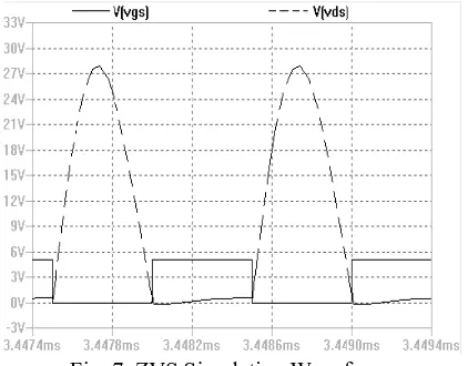
The simulation results obtained from the Class E converter circuit based on the circuit design specifications that has been shown in the previous section. Fig.7 indicates the half sinusoidal waveform of the drain-to source voltage, VDS. The value of
VDS is about 3.0 times greater than the value of VDD
due to the charges stored in the Cshunt increased.
While the square waveform is gate-to-source voltage, VGS, which is specified as VGS=5V. When
the switch is OFF, the current flow through shunt capacitor, Cshunt, produces the voltage across the
capacitor and the drain-to-source voltage. Thus, shunt capacitor, Cshunt shapes the drain-to-source
voltage. The LTspice simulation results agree with the theoretical expectation.
Fig. 7. ZVS Simulation Waveform
4.2 Experimental Results
In order to confirm the theoretical and simulation results, the experimental work has been carried out as shown in Fig. 8. The DC input voltage that is supplied to the Class E converter circuit is 9V at 1MHz operating frequency.
Fig. 8. Class E Converter Circuit
It can be observed from Fig. 9 that the result is approximately similar to the simulation result of Fig. 7. The gate voltage waveform, VGS is 12.9VP-p
while the drain voltage waveform, VDS is 26.1VP-p
which is satisfied the condition of ZVS and ZDS of Class E converter circuit.
Authors in [7] found that there is a difference performance of capacitor compensation between secondary series compensation and secondary parallel compensation. The high peak efficiency of the system can be produced by secondary series topology. On the other hand, high power transfer can be produced by the secondary parallel topology. Hence, the experimental work is carried out to verify the results. Fig. 10 depicts the waveform of series capacitor compensation of the loosely coupled IPT system at 15 mm air gap distance.
Fig. 10. Series Compensation
From the Fig. 10, it can be observed that the peak of voltage transferred is 27V at the primary side (channel 1). Meanwhile, the peak of voltage received is 3V without load at the secondary side (channel 2). So, only small voltage can be received at the secondary side of the IPT system when the capacitor, C2 is connected in series with the
secondary coil, L2. Then, Fig.11 depicts the
waveform of parallel capacitor compensation of the loosely coupled IPT system at 15 mm air gap distance.
Fig. 11. Parallel Compensation
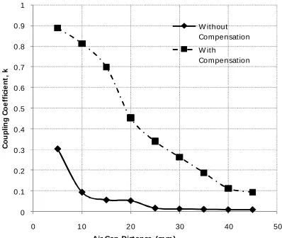
The upper waveform of Fig.11 shows the peak of output voltage of primary side is 27V and the peak of output voltage of secondary side is 22.5V. From the result, we can conclude that the peak of output voltage received by the secondary parallel compensation circuit is much higher than the series compensation circuit in the loosely coupled IPT system and purely sine wave. This is because the resonance inductive coupling can be achieved at the parallel capacitor compensation. Otherwise, it will produce higher peak output voltage at the secondary side of IPT system. Thus, the secondary parallel compensation topology is chosen to be used in this work. Fig. 12 indicates the coupling coefficient, k is determined by an air gap distance between two
Fig. 12. Coupling Coefficient vs. Air Gap Distance
From Fig. 12, the higher coupling coefficient is 0.9 which occurred at 5 mm air gap distance with the capacitor compensation. The coupling coefficient, k can be calculated as in Eq. (17) if the
can be achieved when the secondary coil is connected to the parallel capacitor compensation.
0
1 10 100 1000 10000 100000 1000000
O
Fig. 13. Output Power vs. Load Resistance at 15mm Air Gap Distance
when achieved maximum power transfer. Hence, based on Eq. (18), we obtain 10.1kΩ optimal load resistance that approximately similar to the experimental result. This optimal value only can be achieved when the IPT system met the resonant
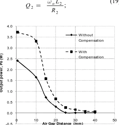
Fig. 14. Output Power vs. Air Gap Distance
From Fig. 14, the output power across 180Ω load resistance has slightly decreased when air gap distance become longer. It validated the theory that the strength of magnetic field becomes weak at longer air gap and cause a low output power of IPT system. The highest maximum output power is 3.7 W, which is occurred at 5mm coil separation. On the other hand, the maximum output power for the circuit without capacitor compensation is 2.4W. However, at the certain limit of the air gap distance, then, the output power is approximately to be a zero and remain constant . This is because, the secondary coil is does not receive the induced voltage from the first coil at that distances any more.
5 Conclusions
In this paper, the Class E converter circuit for inductive power transfer has been introduced at the primary circuit. On the other hand, the voltage doubler and Darlington circuit have been proposed at secondary circuit. The secondary capacitor compensation performance has also been studied. In regard to the best compensation method that yields a better efficiency, the parallel compensation seems give a better result than the serves one. Due to the leakage problem, the highest power that can be transmitted to the load at 15 mm air gap distance is 1.6W. Therefore, the intention future work that should be considered is to design a self-tuning Class E converter circuit to resolve that problem.
6 Acknowledgement
Sincerely to express the appreciation to Universiti Teknikal Malaysia Melaka (UTeM) for funding this work (PJP/2013/FKEKK(10A)/S1177).
References
[1] Jamal, N., S. Saat, and A. Shukor. A study on performances of different compensation topologies for loosely coupled inductive power transfer system. in Control System, Computing and Engineering (ICCSCE), 2013 IEEE International Conference on. 2013. IEEE.
[2] Bosshard, R., Badstubner, U., Kolar, J. W., & Stevanovic, I. Comparative evaluation of control methods for inductive power transfer. in Renewable Energy Research and Applications (ICRERA), 2012 International Conference on. 2012. IEEE. [3] Sivakumar, S. and A. Eroglu. Analysis of
Regular Papers, IEEE Transactions on, 2010. 57(1): p. 299-311.
[4] Sokal, N.O., Class-E RF power amplifiers. QEX Commun. Quart, 2001(204): p. 9-20. [5] Liu, X., Ng, W. M., Lee, C. K., & Hui, S. R.
Optimal operation of contactless transformers with resonance in secondary circuits. in Applied Power Electronics Conference and Exposition, 2008. APEC 2008. Twenty-Third Annual IEEE. 2008. IEEE.
[6] Kazimierczuk, M.K. and D. Czarkowski, Resonant power converters. 2012: John Wiley & Sons.
[7] Prasanth, V., Wireless Power Transfer for E-Mobility. Master of Science Thesis, Delf University of Technology, Faculty of Electrical Engineering, Mathematics and Computer Science, Electrical Power Processing, 2012.
[8] Minsheng, Y., Yaonan, W., Xizheng, Z., & Jianqi, L. Analysis of Reflected Load Model for Inductively Coupled Power Transfer Systems. in Power and Energy Engineering Conference (APPEEC), 2010 Asia-Pacific. 2010. IEEE.
[9] Thian, M. and V. Fusco, Idealised operation of zero-voltage-switching series-L/parallel-tuned Class-E power amplifier. IET circuits, devices & systems, 2008. 2(3): p. 337-346. [10] Kazimierczuk, M. and K. Puczko, Exact
analysis of class E tuned power amplifier at any Q and switch duty cycle. Circuits and Systems, IEEE Transactions on, 1987. 34(2): p. 149-159.
[11] Zhong, W., X. Liu, and S.R. Hui, A novel single-layer winding array and receiver coil structure for contactless battery charging systems with free-positioning and localized charging features. Industrial Electronics, IEEE Transactions on, 2011. 58(9): p. 4136-4144.
[12] Budhia, M., G.A. Covic, and J.T. Boys, Design and optimization of circular magnetic structures for lumped inductive power transfer systems. Power Electronics, IEEE Transactions on, 2011. 26(11): p. 3096-3108.