ContentslistsavailableatSciVerseScienceDirect
Journal
of
Materials
Processing
Technology
j o u r n a l ho m e p age : w w w . e l s e v i e r . c o m / l o c a t e / j m a t p r o t e c
Carbon
nanofiber
assisted
micro
electro
discharge
machining
of
reaction-bonded
silicon
carbide
Pay
Jun
Liew
a,c,
Jiwang
Yan
b,∗,
Tsunemoto
Kuriyagawa
aaDepartmentofMechanicalSystemsandDesign,TohokuUniversity,AramakiAoba6-6-01,Aoba-ku,Sendai980-8579,Japan
bDepartmentofMechanicalEngineering,FacultyofScienceandTechnology,KeioUniversity,Hiyoshi3-14-1,Kohoku-ku,Yokohama223-8522,Japan
cManufacturingProcessDepartment,FacultyofManufacturingEngineering,UniversitiTeknikalMalaysiaMelaka,HangTuahJaya,76100DurianTunggal,Melaka,Malaysia
a
r
t
i
c
l
e
i
n
f
o
Articlehistory: Received4July2012
Receivedinrevisedform26January2013 Accepted3February2013
Available online 11 February 2013
Keywords:
Microelectrodischargemachining Carbonnanofiber
Reaction-bondedsiliconcarbide Ultra-hardceramics
Microfabrication
a
b
s
t
r
a
c
t
Carbonnanofiberassistedmicroelectrodischargemachiningwasproposedandexperimentswere per-formedonreaction-bondedsiliconcarbide.Thechangesinelectrodischargingbehavior,materialremoval rate,electrodewearratio,electrodegeometry,sparkgap,surfacefinish,surfacetopographyandsurface damagewithcarbonnanofiberconcentrationwereexamined.Ithasbeenfoundthattheadditionof carbonnanofibernotonlyimprovestheelectrodischargefrequency,materialremovalrate,discharge gap,butalsoreducestheelectrodewearandelectrodetipconcavity.Bidirectionalmaterialmigrations betweentheelectrodeandtheworkpiecesurfaceweredetected,andthemigrationbehaviorwasstrongly suppressedbycarbonnanofiberaddition.Adhesionofcarbonnanofiberstotheworkpiecesurfaceoccurs, whichcontributestotheimprovementofelectrodischargemachinability.Thesefindingsprovide pos-sibilityforhigh-efficiencyprecisionmanufacturingofmicrostructuresonultra-hardceramicmaterials.
© 2013 Elsevier B.V. All rights reserved.
1. Introduction
Micromachiningofadvancedengineeringceramicsiscurrently gaining interests from multidisciplinary researchers. Reaction-bonded silicon carbide (RB-SiC) is one of the most promising engineeringceramics.Ithasexcellentproperties,suchashigh ther-mochemicalstability,low density,highstiffness, highhardness, highthermalconductivityandlowactivation.RB-SiCisfabricated byinfiltratingmeltedsiliconintoagreenbodyconsistingofcarbon (C)andSiCpowders,followedbyreactionandsinteringprocess atabout1700KtoformnewSiCgrains.Inthisway,averydense materialstructurecanbeproduced(Suyamaetal.,2003).
Duetoits highhardness,RB-SiCis extremely difficulttobe machined.Manyeffortshavebeenmadebypreviousresearchers onabrasivemachiningofRB-SiC.Forexample,Tametal.(2007)
investigatedthelappingandpolishingofRB-SiCusingvariouskinds of abrasives. Klocke and Zunke (2009) foundthat the material removalmechanismsofsiliconbasedceramicsdependstronglyon workpiecematerialproperties,polishingagentsaswellas machin-ingparameters.Generallyspeaking,abrasivemachiningprocesses produce a fine surface finish, but the material removal rate is low.Diamondcuttingof RB-SiCwasrecentlyattemptedbyYan
etal.(2009),whichcouldproduceahighmaterialremovalrate.
∗Correspondingauthor.Tel.:+81455661445;fax:+81455661495. E-mailaddress:[email protected](J.Yan).
However,tool-wearstillremainstobeaprobleminitsindustrial applications.
Electrodischargemachining(EDM)isanalternativemethodto machinehardceramicsmaterials.Acomparativestudyofthe die-sinkingEDMofthreedifferentceramicmaterialswascarriedoutby
PuertasandLuis(2004).Clijstersetal.(2010)manufactured
com-plexpartsonSiSiCmaterialsusingEDM.However,mostceramics arenotsufficientlyconductive,whichisa majorproblemwhen applyingEDMtoceramicsmaterials.Konigetal.(1998)indicated thattheupperlimitofelectricalresistivityforaceramicworkpiece tobemachinedbyEDMis100cm.AspureSiChasafarhigher electricalresistivity(∼105cm),itisimpossibletobemachined
directlybyEDM.ForRB-SiC,duetothepresenceoffreeSi (nor-mallypoly-crystalline)andothersmall-amountadditivesintheSiC bulk,theelectricalconductivitycanbeimprovedtosomeextent
(Wilhelmetal.,1999).Eventhough,theconductivityofRB-SiCis
stillverypoorifcomparedtootherconductivematerials.Hence, theEDMmachiningefficiencyofRB-SiCisextremelylowandthe EDMprocessisunstable.
In order to improve the EDM machinability of materials, a numberofresearchersattemptedaddingconductivepowdersinto dielectricfluids.Forexample,Yeoetal.(2007)added45–55 nm-sizedSiCpowdersintodielectricandfoundthatthesurfacecraters becamesmallerthanthoseproducedinpowderfreedielectricfluid.
Chowetal.(2008)addedSiCpowdersintopurewaterasdielectric
fluidintheEDMoftitaniumalloy,andconfirmedtheimprovement insurfacequalityandmaterialremovalrate.Gunawanetal.(2009)
0924-0136/$–seefrontmatter© 2013 Elsevier B.V. All rights reserved.
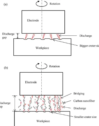
Fig.1.Schematicmodelfor(a)conventionalEDMand(b)carbonnanofiberassistedmicroEDM.
addedmolybdenumdisulfide(MoS2)powdersandimprovedthe materialremovalrateandsurfaceroughnessofCu,brassandCu–W workpiecematerials.Gunawanetal.(2011)alsotriedsuspending nanographite powder in dielectric fluid withthe combination ofultrasonicvibration.Theyfoundthatthemachiningtimewas reducedupto35%.PowderassistedEDMwasalsoappliedtothe EDMofceramicmaterials.Jahanetal.(2010a,b)studiedtheeffect ofaddinggraphite,aluminumandnon-conductivealumina pow-dersinEDMoftungstencarbide ceramics.Theyfoundthatthe graphitepowder provided a smoothsurface and thealuminum powderresultedinhighersparkgapandhighermaterialremoval rate,whereasthealuminapowderhadlittleeffectontheEDM per-formance.Nevertheless,forlow-conductivityorinsulatingceramic materials,itwasdifficulttoobtaingoodmachiningperformanceby powderaddition.Forexample,Tanietal.(2002)usedAl,Gr,Si,Ni, ZrB2 powderstoassisttheEDMofinsulatingSi3N4ceramicsand foundthateventhoughtheremovalratewasincreased,thesurface
roughnesswasbarelyimproved.Thiswasduetothegenerationof longpulsedischargeintheEDMprocess.
Table1
Propertiesofworkpiecematerial(RB-SiC).
Properties Values
Si/SiCvolumeratio(%/%) 12/88
Density(g/cm3) 3.12
Softeningtemperature(◦C) 1375
YoungmodulusE(GPa) 407
BendingstrengthRT(MPa) 780
Thermalexpansioncoefficient(10−6K–1) 3.23
Thermalconductivity(W/mK) 143
Porosity(%) <0.1
workpiecesurfaceroughness,surfacetopographyandsurface dam-agewereinvestigatedexperimentally.
2. Experimentalmethods
2.1. Machinetool
AmicroEDMmachine,PanasonicMG-ED82W,wasusedinthe experiments.ThisEDMmachinehasaresistor–capacitor(RC) cir-cuitforelectro-discharge.Theelectricalcapacitanceisdetermined bycondensersC1–C4,thecapacitiesofwhichare3300pF,220pF, 100pFand10pF,respectively.Themachine enablesboth micro wireEDMandmicrodiesinkingmachining.Themaximumtravel rangesofthemachinetablesare200mminXdirection,50mmin Ydirection,and50mminZdirection,withasteppingresolutionof 0.1m.
2.2. Electrode
Tungstenrodswith300mdiameterswereusedastool elec-trodes. Beforethe EDMof RB-SiC, thetool electrode tips were dressedbyusingwireelectrodischargegrinding(WEDG)inorder toimprovetheirformaccuracy.Electrodedressingwasalso per-formedaftereachEDMcyclebecausethetipelectrode,especially thecorner,willwear.IntheWEDG,abrasswire(diameter100m) withpositiveelectrodepolaritywasusedtomachinethetool elec-trodewhichwasrotatedata rotationspeedof3000rpmbythe machinespindle.UsingtheWEDGfabricatedelectrodes,machining testsofmicrocavitieswereperformedonRB-SiCusingdiesinking EDM,wherenegativeelectrodepolaritywasused.
2.3. Workpiece
TheworkpiecematerialusedintheexperimentswasRB-SiC (JapanFineCeramicsCo.,Ltd.).Theas-receivedsampleswere cylin-derswitha diameterof 30mm and a thicknessof 10mm. The volumeratioofresidualSibondis12%,andtheaveragesizeofthe 6H–SiCgrainsislessthan1m.Sometypicalmaterialproperties ofthesampleareshowninTable1.
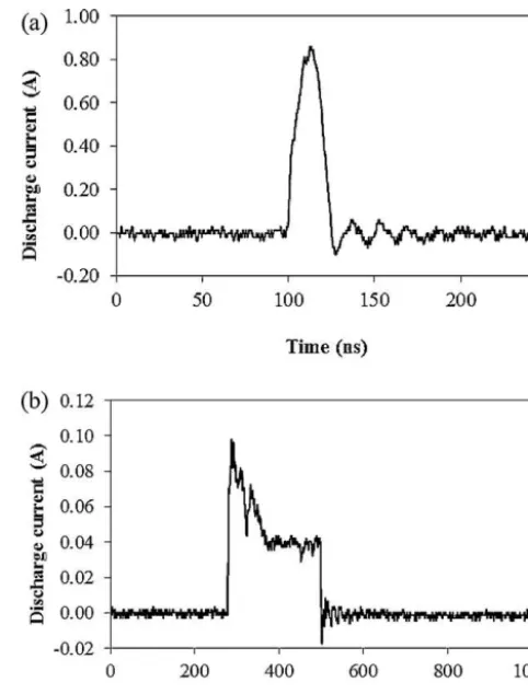
Theelectricalresistivityofthesampleis1453cm.To com-paretheEDMmachinability,a fewpreliminaryEDMtestswere performedontheRB-SiCworkpieceand stainlesssteelSUS304.
Fig.2showsmeasurementresultsofelectricalcurrentsintheEDM ofSUS304andRB-SiC,respectively.Theexperimentwasperformed usingatungstenelectrodewithadiameterof47matavoltage of80Vandacondenserof100pFthatissuggestedbythemicro EDMmachinemanufacturer,andtheelectricalcurrent measure-mentwasperformedusingTektronixTDS2024Bwithcurrentprobe CT-2.ItisclearthatforSUS304,thepulseisverysharpwithapulse widthof25nsandapeakelectricalcurrentof0.9A.Incontrast,for RB-SiCthepulsewidthis220nsandthepeakelectricalcurrentis only0.1A.Thisdistinctdifferenceinelectricalcurrentpulseshape indicatesthattheEDMmachinabilityofRB-SiCisfarlowerthanthe stainlesssteel.
Fig.2. ElectricalcurrentwaveformsinEDMof(a)SUS304and(b)RB-SiC.
2.4. Carbonnanofiber
Carbonnanofibersusedinthis studyare150nmindiameter and6–8minlength.Fig.3showsascanningelectronmicroscope (SEM)micrographofthecarbonnanofibers.Differentfiber concen-trationsrangingfrom0to0.28g/Lwereused.Thedielectricfluid usedwashydrocarbondielectricoilCASTY-LUBEEDS,whichhas ahighflashpoint. Inorder topreparethemixeddielectric,the requiredamountsofcarbonnanofibersanddielectricfluidwere measuredseparately beforebeingmixedtogetherand homoge-nized in a mixer for 20min. This is toensure that the carbon nanofibersareuniformlydispersedinthedielectricfluid.
Table2
Experimentalconditions.
Workpiecematerial RB-SiC
Electrodematerial Tungsten
Polarity Positive(workpiece)
Negative(toolelectrode)
Rotationalspeed 3000rpm
Voltage 110V
Condensercapacitance 3300pF
Feedrate 3m/s
Dielectricfluid EDMoilCASTY-LUBEEDS
Additive Carbonnanofibers
Concentration 0–0.28g/L
Machiningtime 5min
Cavitydepth 20m
2.5. Machiningconditions
Table2showstheexperimentalconditions.Forcomparison,two
typesofEDMtestswerecarriedoutunderdifferentfiber concen-trations:(1)time-controlling method,whereeach trialrunwas performedfordurationof5min,and(2)depth-controllingmethod, wherediesinkingmicroEDMtestswereperformeduntiladepth of20m.Normally,depth-controllingmethodisusedforrough machining(shapegenerating)andtime-controllingmethodisused forfinemachining(surfacefinishing).
2.6. Measurementandevaluation
Surfaceroughnessoftheworkpieceandcross-sectionalprofile ofelectrodetipaftertheEDMtestsweremeasuredusingalaser probeprofilometerNH-3SP(MitakaKoukiCo.Ltd.).The measure-mentofsurfaceroughnesswasperformedacrossthecenterofthe microcavityalongtheradialdirection,andtheevaluationlength was100m.Themachinedsurfaceofthemicrocavitieswerethen examinedusingascanningelectronmicroscope(SEM)andenergy dispersiveX-ray(EDX).Anopticalmicroscopewasusedtomeasure thedimensionoftheelectrodeandthesizeofthecavityaftereach experiment.
3. Resultsanddiscussion
3.1. Electrodischargebehavior
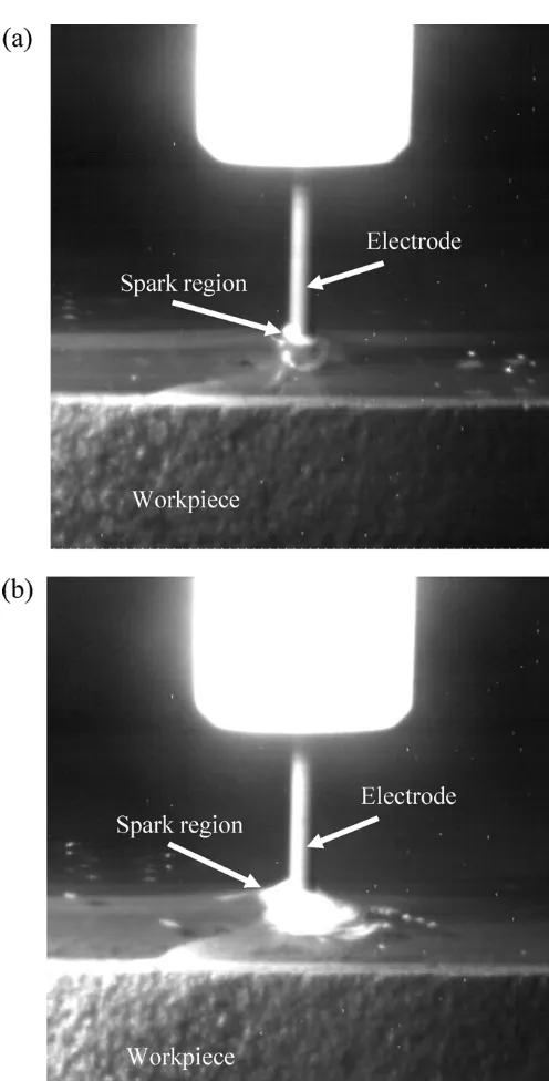
Todirectlyexaminetheeffectofcarbonnanofiberadditionon electrodischargebehavior,ahighspeedcamerasystemwasusedto observetheEDMregion.Fig.4showshighspeedcameraimagesof sparkgenerationduringmicroEDMwithoutcarbonnanofiber addi-tionandwithcarbonnanofiberaddition(concentration0.06g/L), respectively.It is clearthatthespark regionin Fig.4(b) is dis-tinctlybiggerthanthatof(a),indicatingthatelectrodischargehas beensignificantlyactivatedby carbonnanofiber addition.Next, thedischargevoltagewaveformswereobservedusingan oscil-loscopeTexioDCS9515.Fig.5showsthevoltagewaveformsfor microEDMwithoutcarbonnanofiber additionandwithcarbon nanofiberaddition (concentration0.06g/L),respectively. During thesameperiodoftime(1000s),thepulsenumberofdischarge voltagein Fig.5(b) is 37, whilethat in Fig.5(a)is only 2.This resultdemonstratesagainthatduetothecarbonnanofiber addi-tion,theelectrodischargecharacteristicsinEDMofRB-SiChave beengreatlyimproved.ItshouldbenotedthatinFig.5(b),a mul-tipledischargingeffect(severaldischargingpathsaregenerated withinonesingleinputpulse)wasobservedwithinasingleinput pulse,indicatingthatthedischargingenergyhasbeendispersedby thefiberaddition.
Fig.4.HighspeedcameraobservationofsparkgenerationduringmicroEDM:(a) withoutand(b)withcarbonnanofiberaddition.
3.2. Materialremovalrate
Materialremovalrate(MRR)wascalculatedasthevolumeof materialremovedfromworkpieceoveraperiodoftime.Thelaser probeprofilometerNH-3SPwasusedtoscanacrossthemachined area, as shown in Fig.6,and thevolume of material removed wasobtainedbyanalyzingthethree-dimensionalsurface topog-raphy.
0 10 20 30 40 50
0 100 200 300 400 500 600 700 800 900 1000
Discha rg e v o ltag e (V) Time (μs) (a) 0 10 20 30 40 50
0 100 200 300 400 500 600 700 800 900 1000
Discharg e v o ltag e (V) Time (μs) (b)
Fig.5.DischargevoltagewaveformduringmicroEDM:(a)withoutand(b)with carbonnanofiberaddition.
Fig.6.Three-dimensionaltopographyofamachinedcavityforthemeasurementof volumeofmaterialremovedfromworkpiece.
0 0.0005 0.001 0.0015 0.002 0.0025 0.003 0.0035 0.004 0.0045
0 0.05 0.1 0.15 0.2 0.25 0.3
m m ( et ar l a v o me r l ai re t a M 3/m in)
Concentration of carbon nanofibers (g/L) d = 20µm t= 5 min
Fig.7.Effectofcarbonnanofibersconcentrationonmaterialremovalrate.
0
20
40
60
80
100
120
140
0
0.05
0.1
0.15
0.2
0.25
0.3
Electrode wear rate (%)
Concentration of carbon
nanofibers (g/L)
t= 5 min d = 20 µm
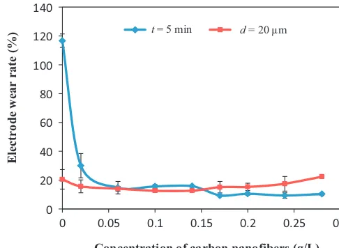
Fig.8. Effectofcarbonnanofibersconcentrationonelectrodewearrate.
of discharge will be increased and the EDM machinability has beenimproved byadding carbon nanofibers intothe dielectric fluid.
Itshouldbenotedthatthereisanoptimumrangeforcarbon nanofiberconcentration.InFig.7,forfiberconcentrationshigher than 0.17g/L, the MRRtends toreduce (forthe depth control-lingmachining)orkeepalmostconstant(forthetime-controlling machining).ThistrendisconsistentwiththatreportedbyJahan
etal.(2010a).Atanexcessivelyhighconcentrationofpowder(in
thiscase,carbonnanofibers)additive,thedepositedpowders can-notbe removedeasilyfromthemachininggapand causedthe secondarysparking.Thissecondarysparkingmakesthemachining unstableandincreasesthemachiningtime,leadingtothereduction ofMRR.
3.3. Electrodewearratio
Electrodewearratio(EWR)isdefinedastheratioofvolume of material removed fromelectrode tothe volume of material removedfromtheworkpieceatthesametimespan.Thechange ofEWRversuscarbonnanofiberconcentrationisdepictedinFig.8. Under thetime-controlling condition,theEWRdropped signifi-cantlywhen thecarbon nanofiberswere added,and then keep constantwhenfurtherincreasingtheconcentrationofthecarbon nanofibers.AsknownfromParamjitetal.(2010),EWRishighwhen usingpuredielectricfluid becauseofthat theionsproducedby theionizationofdielectricfluidhitthetoolelectrodewithhigh momentumandhighenergy,whichcausesrapiderosionofthe toolelectrode.Theadditionofcarbonnanofibersintothedielectric fluidmighthavepreventedtheionizationphenomenon.
It is noticedthat under thedepth-controlling condition,the changeofEWRwasnotsosignificant.Thismightbebecauseof thatthemachiningtimeforaconstantdepthof20mwasshorter ifcompared totime-controlling condition(5min) when carbon nanofiberswereadded.Inthiscase,morematerialswereremoved fromtheworkpiecethanfromtheelectrode.However,whenno carbon nanofibers were added, even though a longer machin-ingtimewastaken,shortcircuitandtoolelectrodebackfeeding occurredfrequently,causingdecreaseinthefrequencyofdischarge and resultinglower erosionoftool electrode. Thus, there is no significantdifferentofEWRwithandwithoutcarbonnanofibers additionunderthedepth-controllingcondition.
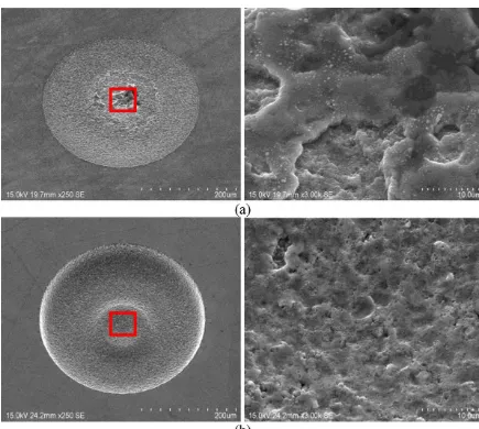
Next, tool electrode geometry after EDM was investigated.
Fig.9. SEMmicrographoftungstenelectrodetipatmachiningdepthof20m:(a) withoutand(b)with0.02g/Land(c)0.10g/Lcarbonnanofibers.
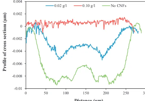
cross-sectional profileofelectrode tipmeasuredbylaser probe profilometerNH-3SPisshowninFig.10.Besidesthecornerwear andendwear,holewearoccurredinthecenteroftungstentip, forming a concave shape (Fig. 9(a)). Interestingly, the concave shapebecameinsignificant,i.e.,theelectrodetipbecameflat,when carbonnanofiberswereaddedinthedielectricfluid(Fig.9(c)).In thesparking gap,thestagnationof debrisoccursintensively in thecenterofthemicrocavity,wherethedebrisparticles inter-actwiththetoolelectrode(EkmekciandSayar,2013),causingthe concavitiesinthecenteroftooltip.Withouttheadditionof car-bonnanofibers,thepileddebrisdensityistypicallyhigherthanthe onewithcarbonnanofibersaddition,causingbiggerconcavityon
-0.01 -0.008 -0.006 -0.004 -0.002 0 0.002 0.004
0 50 100 150 200 250 300
P
rofile of
cr
oss sectiom
(µm
)
Distance (µm)
0.02 g/l 0.10 g/l No CNFs
Fig.10.Comparisonofcrosssectionalprofilesoftungstenelectrodetipaftermicro EDMunderdepthcontrollingcondition.
thetooltip.Increasingcarbonnanofibersconcentrationishelpful forpreventingtheconcavityformation,whereeffectiveflushing takesplaceduetothebiggersparkinggap,andinturn,betterform accuracycanbeobtained.
3.4. Sparkgap
Spark gap wasobtained bymeasuring thediameters of the microcavitiesandtheelectrodesaftereachmachiningtest.The diametersofmicrocavitiesobtainedundertime-controllingand depth-controllingconditionsrangedfrom332mto350m,and from337mto353m,respectively.Fig.11illustratestheeffect of carbon nanofiberconcentrationon spark gap.It isseen that the spark gap increases with the increase of fiber concentra-tion.Theadditionofcarbonnanofiberimprovesthebreakdown strengthofdielectricandcausestheinsulatingstrengthof dielec-tricfluidtoreduce(TzengandChen,2005).Asaresult,abigger spark gap will be maintained, and the debris will be flushed out moreeasily ifcompareto theresultsunderpuredielectric fluid.
When nocarbon nanofibers were added, the discharge gap betweentheelectrodeandworkpieceisextremelysmall,sothatthe debriscouldnotberemovedeffectivelyfromthegap,thusshort cir-cuittakesplacebetweentheelectrodeandworkpiece.Whenshort circuitoccurs,theelectrodewillimmediatelymoveinthereverse
12
17
22
27
32
0
0.05
0.1
0.15
0.2
0.25
0.3
Spark gap
(μ
m
)
Concentratio
n of carbon nanofiber
s (g/L)
d = 20µm t= 5 min
directionofthefeedtomaintainabiggergap(Takashietal.,2008). ThebackfeedingactionwillcausealowMRR.Whenthecarbon nanofiberswereaddedintothedielectricfluid,however,the insu-latingstrengthofdielectricfluidwillbereduced,whichresultsin abiggerdischargegapbetweenthetoolelectrodeandthe work-piece.Inthiscase,debriswillbeeffectivelyremovedfromthegap andshortcircuitwillbeprevented.
3.5. Surfaceroughness
Theeffect of carbon nanofiber concentration onthe surface roughnessofthemachinedsurfaceisshowninFig.12.Underthe time-controllingcondition,thesurfaceroughnesstendstodecrease sharplyat a fiber concentrationof 0.02g/L, and then increases graduallyasfiberconcentrationincreasesfurther.Underthe depth-controllingconditions,thesurfaceroughnessdecreaseswithfiber concentrationuntil0.1g/L,andasfiberconcentrationincreases fur-ther,thesurfaceroughnesstendstoincreaseagain.
Asdemonstrated byParamjitetal. (2010),addinga suitable amountofpowderswillleadtouniformdispersionofdischarge energyinalldirectionsandcauseadecreaseincratersize,thus surfacefinishwillbeimproved.Ata veryhighconcentrationof powderadditive,however,thedielectricmightloseitsabilityto distributeuniformlythepowdermaterials.Therefore,thecarbon nanofibersmayaccumulatetogether,bridgingthedischargegap
0.15
0.2
0.25
0.3
0.35
0.4
0.45
0
0.05
0.1
0.15
0.2
0.25
0.3
Surface roughness (
μ
m
)
Concentration of carbon nanofibers (g/L)
t= 5 min d = 20µm
Fig.12.Effectofcarbonnanofibersconcentrationonsurfaceroughness.
andresultinginarcingandshortcircuitingmorefrequently.This effect will finally increase the surface roughness (Jahan et al.,
2010a).Inthepresentexperiments,theoptimumcarbonnanofiber
concentrationisaround0.02g/Lunderthetime-controlling condi-tions,and0.06–0.1g/Lunderthedepth-controllingconditions.
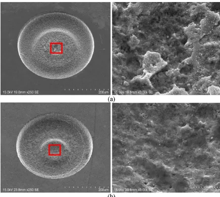
Fig.14. Comparisonofmachinedsurfaceatmachiningdepthof20m:(a)withoutand(b)with0.06g/Lcarbonnanofibers.
3.6. Surfacetopography
Fig.13showsSEMmicrographsofthemachinedmicrocavities obtainedwithandwithoutcarbonnanofiberaddition,respectively, underthetime-controlling conditions.Theleft micrographsare low-magnificationviewsandtherightonesarehigh-magnification viewsof thecenter regionsof theleftones.It is clearthatthe machinedsurfacewithcarbonnanofibersadditive(Fig.13(b))is smoothercomparedtotheoneobtainedwithpuredielectricfluid (Fig.13(a)).Withoutthecarbonnanofibersadditive,thematerials ofRB-SiCwereremovedaslargeflakes,leadingtoverylargecraters (10m level); while with carbon nanofiber addition, the sur-facecratersareextremelysmall(mlevel).Forcomparison,SEM micrographs of the machined micro cavities under the depth-controllingconditionsareshowninFig.14.Similarly,themachined surfacewithfiberadditiveisapparentlysmoother(Fig.14(b))if comparedtotheoneobtainedwithpuredielectricfluid(Fig.14(a)). Asmentioned inSection3.4,withcarbonnanofiber additive inthedielectricfluid,thesparkinggaphasbeenincreased; con-sequentlythedebriscausingsecondarydischargecanbeflushed outfromthegapmoreeasily.Theadhesionofresolidifieddebris onthemachinedsurfaceisreduced,which resultsabetter sur-facetopography.Furthermore,thedischargedistributionbecomes moreuniform,henceuniformlysmallcraterswereproducedonthe machinedsurface(Jahanetal.,2010b).Ifnocarbonnanofiberswere
used,however,thedischargingprocessisunstable,andmaterial isremovedthroughspalling,inwhichsurfacelayersofthe work-piecematerialarefracturedaslargeflakesbythermalshocks.This isdistinctlydifferentfromnormalsparkerosionwhichinvolves melting,dissociation andevaporationofmaterial(Truemanand
Huddleston,2000).Thisresultstronglydemonstratesthatadding
carbonnanofibersinthedielectricfluidishelpfulforimprovingthe surfacefinishofRB-SiC.
Inaddition,itcanbeseenfromFigs.13and14thatcone-shape protrusionswereformedinthecenterofthemicrocavities.This ispresumablybecauseofthedebriswerenotdrawnoutfromthe centerregionandsecondelectricdischargesoccurred.However, thecone-shapeprotrusionswhencarbonnanofibersweremixed inthedielectricfluidweresmallerthanthosewhenpuredielectric fluidwasused.Thesparkinggapinthecarbonnanofibersmixed dielectricfluidisbigger,sothestagnationofdebrisinthecenter ofthemicrocavityisreduced.Theseresultsaresymmetrywith theconcavitythatwasformedinthecenteroftheelectrodetip,as explainedinSection3.3.
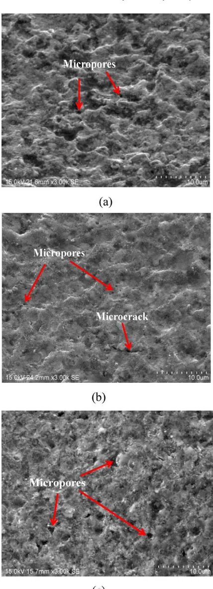
Fig.15.SEMmicrographofmachinedsurface,showingtheexistenceofmicrocracks andmicroporesaftermachiningtimeof5min:(a)withoutand(b)with0.02g/Land (c)0.14g/Lcarbonnanofibers.
cratersproducedwithpuredielectricfluid(Fig.15(a)).Moreover, itisnoteworthythatbyusinghighercarbonnanofiber concentra-tion,suchas0.14g/LasdemonstratedinFig.15(c),thesizeand densityofthemicroporesarebiggercomparedtotheoneobtained withlowercarbonnanofiberconcentration,0.02g/Lasshownin
Fig.15(b). Similartrend wasconfirmed in theresults obtained underthedepth-controllingconditions.
AccordingtoLeeetal.(1988)andLauwersetal.(2004),the for-mationofmicroporesisassociatedwiththeejectionofentrapped gasfromtheredepositedmaterial,andthemicrocracksareformed asaresultofthehighcontractionstressthatexceedstheultimate strengthofthespecimensurface(Ekmekcietal.,2009;Leeetal., 1988).However,carefulexaminationsonthemicrostructurethat produced byhigher carbon nanofiber concentration(Fig.15(c)) revealedthatmicroporesizeisabout5–8timesbiggerthanthe one obtainedwithlower carbon nanofiber concentrations.This phenomenonindicatesthatthemechanismofmicropore forma-tion onRB-SiC ceramic athigh carbon nanofiberconcentration maybedifferentfromthatofthemicroEDMofconductivemetals. Thatis,besidestheejectionofgases,thepreferentialremovalof Sibinderfromtheworkpiecesurfacemayleadtotheformation of micropores. Since the Si matrix, in conjunction with sinter-ingagents,possessesahigherelectricalconductivitythantheSiC grains,itwillbepreferentiallyremovedbymeltingand
vaporiza-tion(Konig etal.,1998)inducedby higherdischargedensityat
highcarbonnanofibersconcentration.Thiseffectwillleave micro-poresonthemachinedsurface,andinturn,increasethesurface roughness.Therefore,optimizingtheamountofcarbonnanofiberis importantforimprovingsurfaceroughnessandpreventingsurface damage.
3.7. Materialmigrationphenomena
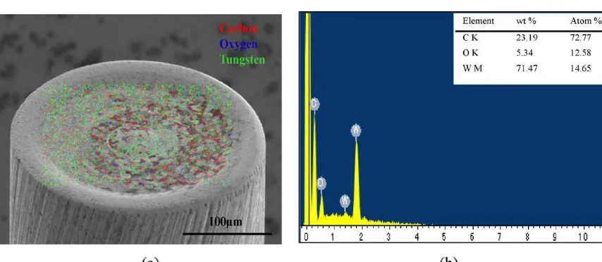
Fig.16showsSEMmicrographandanEDXspectrumofamicro cavitymachinedbymicroEDMwithcarbonnanofiberaddition. Forcomparison,theresultsformicroEDMwithoutfiberaddition areshowninFig.17.InFigs.16(b)and17(b),itcanbeseenthat besidestheparentmaterialsofRB-SiC,suchasCandSi(Ois pre-sumablyfromtheatmosphere),theelectrodematerial tungsten (W)hasbeendetectedonthemachinedworkpiecesurface.This resultindicatesthatthereisamigrationofmaterialfromthe elec-trodetothemachinedsurface,asreportedbySoniandChakraverti
(1996).Inaddition,comparingFigs.16(b)and17(b),itis
notewor-thythatthetungstenmaterialtransferfromtheelectrodetothe workpieceinpuredielectricfluidishigherthantheoneobtained incarbonnanofibermixedfluid.Thisfactdemonstratedthatadding carbonnanofibersindielectricfluidatasuitableconcentrationis helpfulforpreventingmaterialmigration,andinturn,reducestool electrodewear.
Fig.18(a)shows SEMmicrographofatungstenelectrodetip aftermicroEDM,andFig.18(b)showsitsEDXspectrumanalysis results.TheelementChasbeendetectedontheelectrodetipas indicatedinFig.18(a),indicatingthatduringEDMthecarbon ele-mentfromthenanofibers,dielectricoilortheworkpiecematerial hasalsobeenpartiallytransferredtotheelectrodesurface.From thisfact,onecansaythatthematerialmigrationbetweentool elec-trodeandworkpieceisabidirectionalphenomenon.Inaddition, sinceSielementwasnotfoundonthetoolsurface,itis presum-ablethatmaterialmigrationfromtheworkpiecetotheelectrodeis insignificantcomparedtothatfromcarbonnanofibersordielectric oiltoelectrode.
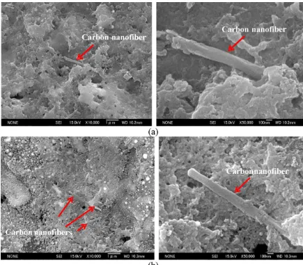
Fig. 19 presents high magnification SEM micrographs (left: 10000×;right:50000×)ofmachinedRB-SiCsurfaceatcarbon
nanofiberconcentrationsof0.14g/Land0.24g/L,respectively.It was found that a few carbon nanofibers have been deposited onto the workpiece surface after the EDM process. Similarly,
Ekmekciand Ersoz (2012) alsoreported that cubic shapedSiC
Fig.16.(a)SEMmicrographand(b)EDXspectrumanalysisofamachinedcavityatcarbonnanofiberconcentrationof0.28g/L.
morefibers aredeposited. Thefiberadhesiontotheworkpiece wassostrongthat theycouldnot beremovedeven the work-piece was washed in acetone using an ultrasonic cleaner. The adheredcarbonnanofibersmaysignificantlyimprovetheelectrical
conductivity of the workpiece surface, which might help to improve the EDM machinability of this material. The material migrationphenomenonwillbefurtherinvestigatedinourfuture work.
Fig.17.(a)SEMmicrographand(b)EDXspectrumanalysisofamachinedcavitywithoutcarbonnanofiber.
Fig.19. SEMmicrographsofmachinedsurfacesaftermachiningfor5minatdifferentcarbonnanofibersconcentrations:(a)0.14g/Land(b)0.24g/L.
4. Conclusions
CarbonnanofiberassistedmicroEDMofRB-SiCwasproposed. Theeffectofcarbonnanofiberadditionontheelectrodischarge behavior,material removalrate,electrode wearratio,electrode geometry,sparkgap,surfaceroughness,surfacetopography,and surfacedamagewasinvestigated.Themajorconclusionsare sum-marizedasfollows:
1.Addingcarbon nanofibersintothe dielectricfluid can signif-icantlyimprovetheelectrodischargefrequency,and inturn, improvethematerialremovalrateandsparkgap.
2.The EWR drops significantly with the increase of carbon nanofiberconcentration,especiallyunderthetime-controlling conditions.
3.Increasingcarbonnanofiberconcentrationishelpfultoprevent tooltipconcavityformation,andinturn,improvesformaccuracy ofmicrocavity.
4.Without carbon nanofiber addition, theRB-SiC material was removedbyspallingoflargeflakes,causinglargesurfacecraters. Withfiberaddition,however,thecratersizecouldbe dramati-callyreduced.
5.Surfacefinishcanbeimprovedbyaddingcarbonnanofibersin thedielectricfluid.Thelowestsurfaceroughnesswasachieved atafiberconcentrationof0.02–0.1g/L.
6.ThemechanismofmicroporeformationonRB-SiCathigh car-bonnanofiber concentrationinvolvespreferentialremoval of siliconbinder,apartfromtheejectionofgasesinEDMofmetal materials.
7.Carbonnanofiberswerepartiallyadheredtotheworkpiece sur-face,especiallywhenahighconcentrationofcarbonnanofibers wasused.
8.Thereisabidirectionalmaterialmigration betweenthe elec-trodeandtheworkpiecesurface.Addingcarbonnanofibersin thedielectricfluidatasuitableconcentrationishelpfulfor pre-ventingthematerialmigration.
References
Chow,H.M.,Yang,L.D.,Lin,C.T.,Chen,Y.F.,2008.TheuseofSiCpowderinwateras dielectricformicro-slitEDMmachining.JournalofMaterialsProcessing Tech-nology195,160–170.
Clijsters,S.,Liu,K.,Reynaerts,D.,Lauwers,B.,2010.EDMtechnologyand strat-egydevelopmentforthemanufacturingofcomplexpartsinSiSiC.Journalof MaterialsProcessingTechnology210,631–641.
Ekmekci,B.,Sayar,A.,2013.Debrisandconsequencesinmicroelectricdischarge machiningofmicroholes.InternationalJournalofMachineToolsand Manufac-ture65,58–67.
Ekmekci,B.,Sayar,A.,Opoz,T.T.,Erden,A.,2009.Geometryandsurfacedamagein microelectricaldischargemachiningofmicro-holes.JournalofMicromechanics andMicroengineering19,105030.
Gunawan,S.P.,Mahardika,M.,Hamdi,M.,Wong,Y.S.,Mitsui,K.,2009.Effectof micro-powdersuspensionandultrasonicvibrationofdielectricfluidin micro-EDMprocesses–Taguchiapproach.InternationalJournalofMachineToolsand Manufacture49,1035–1041.
Gunawan,S.P.,Muslim, M.,Hamdi,M.,Wong,Y.S., Mitsui,K.,2011. Accuracy improvementinnanographitepowdersuspendeddielectricfluidformicro elec-tricaldischargemachiningprocesses.TheInternationalJournalofAdvanced ManufacturingTechnology56,143–149.
Jahan,M.,Rahman,M.,Wong,Y.,2010a.Modelling andexperimental investi-gationonthe effectofnanopowder mixeddielectricin micro electrodis-charge machining of tungsten carbide. Proceedings of the Institution of Mechanical Engineers, PartB: Journal EngineeringManufacture 224 (11), 1725–1739.
Jahan,M.,Rahman,M.,Wong,Y.,2010b.Studyonthenano-powder-mixed sink-ingandmillingmicro-EDMofWC–Co.TheInternationalJournalofAdvanced ManufacturingTechnology53,167–180.
Klocke,F.,Zunke,R.,2009.Removalmechanisms inpolishingofsiliconbased advancedceramics.AnnalsoftheCIRP58(1),491–494.
Konig,W.,Dauw,D.,Levy,G.,Panten,U.,1998.EDM-futurestepstowardsthe machiningofceramics.AnnalsoftheCIRP37(2),623–631.
Lauwers,B.,Kruth,J.P.,Liu,W.,Eeraerts,W.,Schacht,B.,Bleys,P.,2004.Investigation ofmaterialremovalmechanisminEDMofcompositeceramicmaterials.Journal ofMaterialsProcessingTechnology149,347–352.
Lee,L.C.,Lim,L.C.,Narayanan,V.,Venkatesh,V.C.,1988.Quantificationofsurface damageoftoolsteelsafterEDM.InternationalJournalofMachineToolsand Manufacture28(4),359–372.
Paramjit, S., Anil,K., Naveen,B., Vijay,K., 2010. Some experimental investi-gation onaluminium powder mixed EDM on machining performanceof hastelloysteel.InternationalJournalofAdvancedEngineeringTechnology1/2, 28–45.
Puertas,I.,Luis,C.J.,2004.Astudyontheelectricaldischargemachiningof conduc-tiveceramics.JournalofMaterialsProcessingTechnology153/154,1033–1038. Soni,J.S.,Chakraverti,G.,1996.Experimentalinvestigationonmigrationofmaterial duringEDMofdiesteel(T215Cr12).JournalofMaterialsProcessingTechnology 56,439–451.
Suyama,S.,Kameda,T.,Itoh,Y.,2003.Developmentofhigh-strength reaction-sinteredsiliconcarbide.DiamondandRelatedMaterials12,1201–1204. Takashi,E.,Takayuki,T.,Kimiyuki,M.,2008.StudyofvibrationassistedmicroEDM
–theeffectofvibrationonmachiningtimeandstabilityofdischarge.Precision Engineering32,269–277.
Tani,T.,Fukuzawa,Y.,Nambu,K.,Mori,N.,2002.MachiningphenomenainEDM ofinsulatingceramicswithpowdermixedoil.JournaloftheJapanSocietyof ElectricalMachiningEngineers36(81),39–46.
Tam,H.Y.,Cheng,H.B.,Wang,Y.W.,2007.Removalrateandsurfaceroughnessin thelappingandpolishingofRB-SiCopticalcomponents.JournalofMaterials ProcessingTechnology192/193,276–280.
Trueman,C.S.,Huddleston,J.,2000.MaterialremovalbyspallingduringEDMof ceramics.JournalofEuropeanCeramicSociety20,1629–1635.
Tzeng,Y.F.,Chen,F.C.,2005.Investigationintosomesurfacecharacteristicsof electri-caldischargemachinedSKD-11usingpowder-suspensiondielectricoil.Journal ofMaterialsProcessingTechnology170,385–391.
Wilhelm,M.,Kornfeld,M.,Wruss,W.,1999.DevelopmentofSiC–Sicompositeswith fine-grainedSiCmicrostructures.JournaloftheEuropeanCeramicSociety19, 2155–2163.
Yan,J.,Zhang,Z.,Kuriyagawa,T.,2009.Mechanismformaterialremovalindiamond turningofreaction-bondedsiliconcarbide.InternationalJournalofMachine ToolsandManufacture49,366–374.