SINGLE STAGE RF AMPLIFIER AT 5.8GHZ ISM BAND WITH
IEEE 802.11a STANDARD
A. R. Othman
1, I. M. Ibrahim
2, M. S. A. S. Samingan
3, A. A. A. Aziz
4, M. F. M.
Selamat
5, H. C. Halim
61,2,3,4,5,6
Fakulti Kejuruteraan Elektronik Dan Kejuruteraan Komputer, Universiti Teknikal Malaysia Melaka, 75450 Ayer Keroh, Melaka.
Email: [email protected], [email protected]
Abstarct - This paper describes the circuit design and measurement of a single stage RF amplifier for 5.8 GHz-band with IEEE 802.11a standards for WLAN applications. The circuit was simulated using Ansoft Designer where a 14dB of gain; input and output return loss less than -10dB were observed. The GaAs Hetrojunction FET (HFET), capacitors and resistors are combined with the microstrip line pattern by silver epoxy. A 1dB output power compression point (P1dB) of 17dBm and
14.56dB of gain when -1dBm power injected under 6V and ½ Idss biasing are measured.
Index Terms: RF Amplifier; Gain; Matching Circuit; Wireless LAN.
I. INTRODUCTION
Current solutions exploit the worldwide license-free 2.4 GHz frequency band. Unfortunately, many applications nearly overcrowd this band such as high-power microwave ovens, cordless phones, Bluetooth® and HomeRF applications, WLAN, game pads, etc. As a consequence, significant RF interference is present within the 2.4 GHz band [1]. Recently, wireless LAN system have been developed for the C-band (4~8 GHz) frequency. Proposals for wireless data system in the C-band range such as 5.8 GHz (Wireless LAN for U.S.A) and 5.2 GHz (Hiper LAN for Europe) have been submitted [2]. The license-free 5.8 GHz frequency band provides wider spectrum frequency. Furthermore, investigations showed that 5 GHz applications in narrow surroundings can provide better performance than 2.4 GHz applications as the shorter wave length propagates farther. In addition, 5.8 GHz system
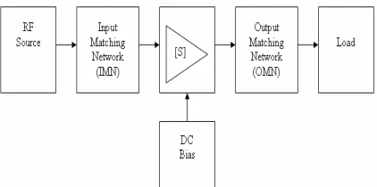
nearly always be operated at higher data rates than 2.4 GHz systems in form of bandwidth [3]. The power amplifier is the most important and expensive device in the RF block of Wireless LAN system [4]. Like all other amplifiers, stability is a major concern [5]. This paper is focused on the development of RF amplifier for point-to-point WLAN application. A single-stage RF amplifier is fabricated using GaAs HFET on microstrip substrate. The size of the circuit is reduced by utilizing high dielectric substrate. Figure 1 shows the block diagram of RF amplifier module.
Fig. 1. Schematic diagram of RF amplifier module
The RF amplifier consists of input and output matching network as passive part and amplifier chip driven by DC bias circuit as an active part. The impedance of the circuit is relatively 50 .
II. CIRCUIT DESIGN
In short, basic concept of high frequency amplifier design is matching input/output of transistor for high frequency having [S] frequency characteristics at a specific DC-bias point with source impedance and load impedance. I/O matching circuit is essential to reduce unwanted reflection of signal and to
improve efficiency of transmission from source to load [6].
The DC bias circuits are designed not to disturb the RF performance [4]. Bias circuit was set at 6V and ½ Idss to operate a HFET EPA 018A-70 at Class A using voltage regulator. This method can achieve high linearity using optimal power back off from the power compression point while maintaining high efficiency [7]. One of the most important factors in high frequency amplifier design is to determine stability of the given bias frequency. Equations in Table I are used to determine the stability of the amplifier. RF amplifier need to be in unconditionally stable where Stability Factor, K higher than 1 with Delta Factor must be smaller than 1, otherwise the amplifier is considered potentially unstable.
TABLE I
STABILITY DETERMINATION BY FORMULA
Stability Criteria
Unconditionally
stable
1
>
K
&
|
∆
|
<
1
Potentially unstable
K
>
1
&
|
∆
|
>
1
or1
<
K
&
|
∆
|
<
1
Stability Factor
|
|
2
|
|
|
|
|
|
1
21 12 2 2 22 2 11S
S
S
S
K
=
−
−
+
∆
Delta Factor
∆
=
S
11S
22−
S
12S
21The input and the output circuits should be matched each other to deliver maximum power to the load. After stability of active device is determined, input/output matching circuits should be designed so that reflection coefficient of each port can be correlated with conjugate complex number as given in equations (1) and (2). L L S IN
S
S
S
S
Γ
−
Γ
+
=
Γ
=
Γ
22 21 12 11 *1
(1)
S S L OUT
S
S
S
S
Γ
−
Γ
+
=
Γ
=
Γ
11 21 12 22 *1
(2)By combining the two formulas above, reflection coefficient of input/output matching circuits are determined by equations (3) and (4) and the substitution as in equation (5).
1 2 1 2 1 1
2
|
|
4
C
C
B
B
SM−
−
=
Γ
(3)2 2 2 2 2 2
2
|
|
4
C
C
B
B
LM−
−
=
Γ
(4)
Where
|
|
|
|
|
|
1
|
|
|
|
|
|
1
21 12 22 11 * 11 22 2 * 22 11 1 2 2 11 2 22 2 2 2 22 2 11 1S
S
S
S
S
S
C
S
S
C
S
S
B
S
S
B
−
=
∇
∇
−
=
∇
−
=
∆
−
−
+
=
∆
−
−
+
=
(5)The above formulas give power and load reflection coefficients to obtain maximum power gain. It can be seen that matching circuit is designed with scattering coefficient determined by the bias and frequency for the given active device.
III. SIMULATION
TABLE II
DUROID 5880 TLY-5A-0200-CH/CH SUBSTRATE PARAMETERS
Dielectric Metalization
Material Resistivity Thickness Unit
H = 0.508mm
r = 2.17 TAND = 0.0018 (5.8GHz)
Cooper 1.72414 0.0175 mm
The comparison between simulated result and original parameters from data sheet can be simplified as shown in Table III.
TABLE III
S-PARAMETER COMPARISON BETWEEN DATA SHEET AND SIMULATION AT 5.8GHZ
S-Parameter Data Sheet (at 5.8GHz)
Simulation (at 5.8GHz)
S11 -2.24dB -10.96dB
S12 -26.26dB -23.78dB
S21 12.07dB 14.56dB
S22 -3.32dB -4.86dB
From the simulated circuit, the stability, K of the circuit is 1.02. Usually, as long as the Stability Factor and Delta Factor are known as unconditionally stable, the stability circle is not necessary to be proved because the amplifier is stable at all area within the smith chart [8].
IV. FABRICATION AND
MEASUREMENT
Fabrication was accomplished by a manufacturer because lack of instruments and tools for this purpose. The designed circuit was also tuned and optimized by the manufacturer in order to get an optimum layout. Somehow, the performances of the simulated circuit are remained.
During measurement process, losses affected the result; some of the losses are possible caused by conductor, dielectric and radiation mechanisms. So the designed amplifier has a small signal gain of 14.56dB better than two-stages PA reported with 6.5dB and 6.2dB [9][10]. The input and output return loss are -10.239dB and -10.937dB respectively at 5.8GHz
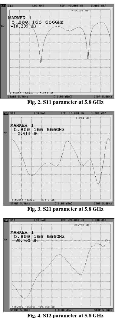
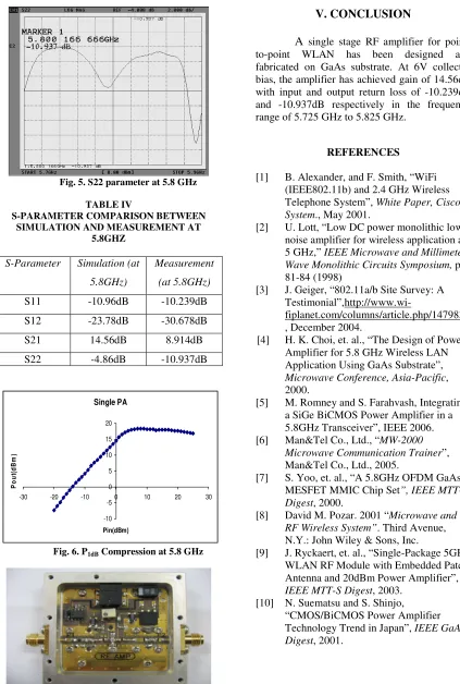
frequency with operating bias of Vds=6V and Ids = 1/2Idss. Figure 2, 3, 4 and 5 are graph of S-Parameter of the RF amplifier measured using Network Analyzer. Table IV is comparison between measured and simulated S-Parameter at 5.8 GHz. This amplifier performed a 1dB compressed output power of 17dBm over 20dBm of EPA 018A-70 maximum output as shown in Figure 6. Figure 7 is the fabricated RF amplifier on Duroid 5880 microstrip substrate.
Fig. 2. S11 parameter at 5.8 GHz
Fig. 3. S21 parameter at 5.8 GHz
Fig. 5. S22 parameter at 5.8 GHz
TABLE IV
S-PARAMETER COMPARISON BETWEEN SIMULATION AND MEASUREMENT AT
5.8GHZ
S-Parameter Simulation (at 5.8GHz)
Measurement (at 5.8GHz)
S11 -10.96dB -10.239dB
S12 -23.78dB -30.678dB
S21 14.56dB 8.914dB
S22 -4.86dB -10.937dB
Single PA
-10 -5 0 5 10 15 20
-30 -20 -10 0 10 20 30
Pin(dBm)
P
o
u
t(
d
B
m
)
Fig. 6. P1dB Compression at 5.8 GHz
Fig. 7. Fabricated RF amplifier
V. CONCLUSION
A
single stage RF amplifier for point-to-point WLAN has been designed and fabricated on GaAs substrate. At 6V collector bias, the amplifier has achieved gain of 14.56dB with input and output return loss of -10.239dB and -10.937dB respectively in the frequency range of 5.725 GHz to 5.825 GHz.REFERENCES
[1] B. Alexander, and F. Smith, “WiFi (IEEE802.11b) and 2.4 GHz Wireless Telephone System”, White Paper, Cisco System., May 2001.
[2] U. Lott, “Low DC power monolithic low noise amplifier for wireless application at 5 GHz,” IEEE Microwave and Millimeter-Wave Monolithic Circuits Symposium, pp. 81-84 (1998)
[3] J. Geiger, “802.11a/b Site Survey: A
Testimonial”,http://www.wi-fiplanet.com/columns/article.php/1479831 , December 2004.
[4] H. K. Choi, et. al., “The Design of Power Amplifier for 5.8 GHz Wireless LAN Application Using GaAs Substrate”,
Microwave Conference, Asia-Pacific, 2000.
[5] M. Romney and S. Farahvash, Integrating a SiGe BiCMOS Power Amplifier in a 5.8GHz Transceiver”, IEEE 2006. [6] Man&Tel Co., Ltd., “MW-2000
Microwave Communication Trainer”, Man&Tel Co., Ltd., 2005.
[7] S. Yoo, et. al., “A 5.8GHz OFDM GaAs MESFET MMIC Chip Set”, IEEE MTT-S Digest, 2000.
[8] David M. Pozar. 2001 “Microwave and RF Wireless System”. Third Avenue, N.Y.: John Wiley & Sons, Inc.
[9] J. Ryckaert, et. al., “Single-Package 5GHz WLAN RF Module with Embedded Patch Antenna and 20dBm Power Amplifier”,
IEEE MTT-S Digest, 2003. [10] N. Suematsu and S. Shinjo,