1
Simulation of Single Stage Cascode Low Noise Amplifier at 5.8GHz Using
T-Matching Network
Ibrahim A.B,Husain M.N,Othman A.R,Johal M.S
Faculty of Electronic and Computer Engineering
Universiti Teknikal Malaysia Melaka
[email protected],[email protected]
Abstract
This paper presents a 5.8 GHz single stage cascode low noise amplifier using T-matching techniques for IEEE 802.16 standard. The amplifier use FHX76LP Low Noise SuperHEMT FET. The design simulation process is using Advance Design System (ADS) software. The cascode low noise amplifier (LNA) produced gain of 17.21dB and noise figure (NF) at 0.845dB. The input reflection (S11) and output return loss (S22) are -12.71dB
and -15.52dB respectively. The bandwidth of the amplifier is 1GHz. The input sensitivity is complying with the IEEE 802.16 standards.
Keywords: Cascode LNA, WiMAX, Radio Frequency, T-Matching Network
1. Introduction
Recently, the market of wireless communication system is growing rapidly. Owing to market demands, there exist various wireless communication systems blooming for different frequency bands and different application. WiMAX, which is short for Worldwide Interoperability for Microwave Access, is a novel wireless communication technology. It is an attractive technology due to the high transmitting speed (up to 70Mbps) and long transmitting distance (up to 30 mile). The system bases on IEEE 802.16 standards and uses several bands (2.3-2.7 GHz, 3.4-3.6 GHz and 5.1-5.8GHz) to transmit data. The design of the front-end low noise amplifier (LNA) is one of the challenges in radio frequency (RF) receivers, which needs to provide good input impedance match, enough power gain and low noise figure (NF) within the required band [1].
Many high gain amplifier topologies have been proposed as a way to satisfy the requirement for low power dissipation as well as good performances. The cascode topology is results in a higher gain, due to the increase in the output impedance, as well as better isolation between the input and output ports. [2-6].In this work, a single cascode LNA topology is proposed.
2. Theoretical
Basically, for the design of an amplifier, the input and output matching network are designed to achieve the required stability, small signal gain, and bandwidth. Super high frequency amplifier is a typical active circuit used to amplify the amplitude of RF signal. Basic concept and consideration in design of super high frequency amplifier is presented below. For the LNA designed, the formula and equation were referred to [3]. Figure 1, shows a typical single-stage amplifier including input/output matching networks.
2
The basic concept of high frequency amplifier design is to match input/output of a transistor at high frequencies using S parameters frequency characteristics at a specific DC-bias point with source impedance and load impedance. I/O matching circuit is essential to reduce unwanted reflection of signal and to improve efficiency of transmission from source to load [3-4].
2.1. Power Gain
Several power gains were defined in order to understand operation of super high frequency amplifier, as shown in Figure 2, power gains of 2 port circuit network with power impedance or load impedance at power amplifier represented with scattering coefficient are classified into Operating Power Gain, Transducer Power Gain and Available Power Gain [3-4].
Figure 2: I/O circuit of 2-port network
2.2. Operating Power Gain
Operating power gain is the ratio of power (PL)
delivered to the load (ZL) to power (Pin) supplied to 2
port network. Power delivered to the load is the difference between the power reflected at the output port and the input power, and power supplied to 2-port network is the difference between the input power at the input port and the reflected power. Therefore, Operating Power Gain is represented by
)
1
(
|
1
|
|
|
1
|
|
|
|
1
1
supplied
2 22 2 2 21 2 L L in in L PS
S
P
P
a mplifier
the
to
power
loa d
the
to
delivered
Power
G
Where,
in indicates reflection coefficient of load at theinput port of 2-port network and
s is reflectioncoefficient of power supplied to the input port.
2.3. Transducer Power Gain
Transducer Power Gain is the ratio of
P
avs ,maximum power available from source to
P
L, power delivered to the load. As maximum power is obtained when input impedance of circuit network is equal to conjugate complex number of power impedance, ifin
=
s, transducer power gain is represented by(2)
Where,
L indicates load reflection coefficient.2.4. Available Power Gain
Available Power Gain, G is the ratio ofA
P
avs, poweravailable from the source, to
a vn
P , power available from
2-port network, that is,
a vs a vn A
P P
G . Power gain is Pa vn
when in
=
s
*
. Therefore Available Power Gain is given by:
(3)
That is, the above formula indicates power gain when input and output are matched [4].
2 21 12 22 11 2 2 2 21 | ) ( ) 1 )( 1 ( | ) | | 1 )( | | 1 ( | | L S L S L S a vs L T S S S S S P P source the from Ava ila ble Power loa d the to delivered Power G 2 22 2 21 2 11 2 | 1 | 1 | | | 1 | | | 1 L S S avs avn A S S S P P source the from a va ila ble Power
a mplifier the
3
2.5. Noise FigureSignals and noises applied to the input port of amplifier were amplified by the gain of the amplifier and noise of amplifier itself is added to the output. Therefore, SNR (Signal to Noise Ratio) of the output port is smaller than that of the input port. The ratio of SNR of input port to that of output port is referred to as noise figure and is larger than 1 dB. Typically, noise figure of 2-port transistor has a minimum value at the specified admittance given by formula:
)
4
(
|
|
2m in s opt
S N
Y
Y
G
R
F
F
For low noise transistors, manufactures usually
provide
F
m in,
R
N,
Y
opt by frequencies. N defined by formula for desired noise figure:)
5
(
|
1
|
/
4
|
|
1
|
|
2 0 m in 2 2 opt N S opt sZ
R
F
F
N
2.6. Condition for Matching
The scattering coefficients of transistor were determined. The only flexibility permitted to the designer is the input/output matching circuit. The input circuit should match to the source and the output circuit should match to the load in order to deliver maximum power to the load. After stability of active device is determined, input/output matching circuits should be designed so that reflection coefficient of each port can be correlated with conjugate complex number as given below [5]:
(6)
(7)
The noise figure of the first stage of the receiver overrules noise figure of the whole system. To get minimum noise figure using transistor, power reflection coefficient should
match with
opt and load reflection coefficient shouldmatch with
out*s
=
opt (8)
s s out LS
S
S
S
11 21 12 22 *1
(9)3. Design of LNA
The cascode LNA was design based on the S-parameter were obtained from calculation and simulation process using ADS. The S-parameter for cascode shown in Table 1.
Table 1: S-Parameter for LNA
S11 S12 S21 S22
5.8GHz 0.715 0.055 4.307 0.404
Angle -82.739 43.240 87.684 -49.997
The overall performance of the LNA is determined by calculating the transducer gain GT, noise figure F and the
input and output standing wave ratios, VSWRIN and
VSWROUT. The optimum, Γopt and ΓL were obtained as
Γopt = 17.949 + j48.881 and ΓL = 79.913- j7.304.
The complete schematic of the 5.8GHz a cascode low noise amplifier is shown in figure 3. Gate and drain of transistor M1 being shorted, it is called enhancement load device. Source of Transistor M2 was inserted with inductor L=0.045nH, it is called inductive source degeneration. The values of passive elements in the input matching network are L1=678.8pH, L2=2.92nH and
C1=321.5fF and the values of passive elements in the
output matching are C2=798.8fF, C3=880.95fF and
L3=2.07nH. Parameters L4=1.13nH, L5=2.74nH, C4 and
C5=1pF act as a bias network. From simulation, it was
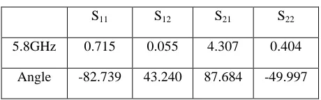
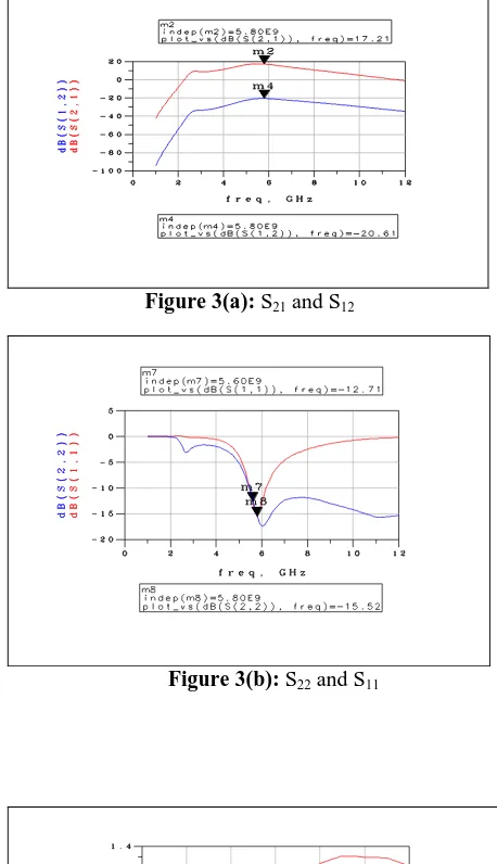
recorded that the amplifier gain S21 was 17.21 dB. The
4
(NF) was 0.845dB and the output insertion loss S22 was
-15.52dB. The reflected loss S12 was -20.61dB.
These
values were within the design specification and were
accepted.
Figure 3: Complete schematic of the 5.8GHz LNA
4. Simulation of Results
The Figure 3(a) is shows a graph of forward gain S21
and input insertion loss S12 while; Figure 3(b) is shows a
graph of reflection loss S11 and output of insertion loss S22.
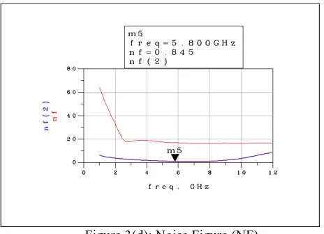
Graph 3(c) and 3(d) shows the stability and noise figure respectively. It is simulated using Advanced Design System software as well as tuning for the optimum noise figure and gain. The resultant of s-parameters is shown in Table 2.
Table 2: S-Parameter after matching process
Figure 3(a): S21 and S12
Figure 3(b): S22 and S11
Figure 3(c):Stability of LNA
5
Figure 3(d): Noise Figure (NF)
5. Conclusions
This paper presents a 5.8GHZ LNA design and simulation using Advance Simulation System (ADS) software. The design was tuned using optimization tools in ADS such that the final design was improved in both gain and noise figure. The cascode topology was chosen for this design as it offers improved gain, reverses isolation and reduces the miller effect. The cascode amplifier use FHX76LP Low Noise SuperHEMT FET. At 5.8GHz, this LNA was recorded that the amplifier gain S21 was 17.21 dB. The input insertion loss S11 was
-12.71dB and the output insertion loss S22 was -15.52dB.
The reflected loss S12 was -20.61dB.The stability (K) and
noise figure (NF) was 1.01dB and 0.845 respectively.
REFERENCES
[1] Ruey-Lue Wang, Shih-Chih Chen,Cheng-Lin Huang,Chien-Hsuan Lie,Yi-Shu Lin. "2-6GHz Current-reused LNA With Transformer-type Inductors." IEEE 2008.
[2] Leon, Michael Angelo G.Lorenzo and Maria Theresa G.De. "Comparison of LNA Topology for Wimax Application in a Standard 90-nm CMOS Process." 12th International Conference
on Computer Modelling and Simulation. 2010. pp-642-647.
[3] M.Pozar, David. Microwave and RF Wireless System. Third Avenue,N.Y.John Wiley & Sons,in, 2001.
[4] Gonzalez, Guillermo. Microwave Transistor Amplifier. 1996.
[5] Othman A.R, Hamidon A.H,Ting J.T.H and Mustaffa M.F. "High Gain Cascaded Low Noise Amplifier Using T-Matching Network." 4th ISBC 2010.