Low Noise Amplifier at 5.8GHz with Cascode and Cascaded
Techniques Using T-Matching Network for Wireless Applications
Ibrahim A.B, Hussain M.N, Othman A.R, Johal.M.S Faculty of Electronic and Computer Engineering
Universiti Teknikal Malaysia Melaka Email: [email protected], [email protected]
Abstract
This project present a design of a 5.8 GHz low noise amplifier (LNA) design with cascode and cascaded techniques using T-matching network applicable for IEEE 802.16 standard. The amplifier use FHX76LP Low Noise SuperHEMT FET. The LNA designed used T-matching network consisting of lump element reactive element at the input and the output terminal. The cascode and cascaded low noise amplifier (LNA) produced gain of 36.8dB and noise figure (NF) at 1.3dB. The input reflection (S11) and output return loss (S22) are -11.4dB and -12.3dB respectively. The bandwidth of the amplifier is more than 1GHz. The
input sensitivity is compliant with the IEEE 802.16 standards.
Keyword: Cascode and Cascade LNA, Radio Frequency, T -Matching Network
1. Introduction
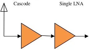
The number of systems that use radio frequency (RF) links is increasing quickly. At the same time, the number of standards for such systems is increasing quickly as well. To make this possible the number of frequency band dedicated for wireless communication has also increased [1]. WiMAX, which is short for Worldwide Interoperability for Microwave Access, is a novel wireless communication technology. It is an attractive technology due to the high transmitting speed (up to 70Mbps) and long transmitting distance (up to 30 mile). The system bases on IEEE 802.16 standards and uses several bands (2.3-2.7 GHz, 3.4-3.6 GHz and 5.1-5.8GHz) to transmit data. The design of the front-end low noise amplifier (LNA) is one of the challenges in radio frequency (RF) receivers, which needs to provide good input impedance match, enough power gain and low noise figure (NF) within the required band [2].Many high gain amplifier topologies have been proposed as a way to satisfy the requirement for low power dissipation as well as good performances. The cascode with cascaded techniques to produces results in a higher bandwidth and gain, due to the increase in the output impedance, as well as better isolation between the input and output ports. [3-7]. Most of the single stage LNA device in the review could only around 20 dB gain. It was proposed that the low noise amplifier should have a gain of at least 30 dB. By taking consideration the extension of communication distance of up to 50 km. A budgeted high gain LNA will ensure a good signal to noise separation for further amplification. For this gain of 30 dB, a cascode with cascaded amplifier is introduced for the LNA as shows in figure 1.
Figure 1. Cascode and Cascaded LNA
2. Theoretical Aspects
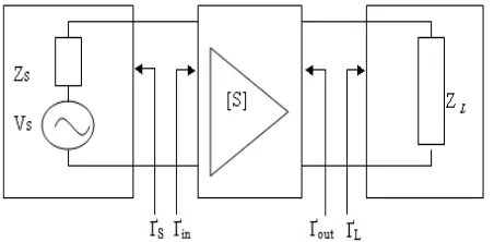
Basically, for the design of an amplifier, the input and output matching network are designed to achieve the required stability, small signal gain, and bandwidth. Super high frequency amplifier is a typical active circuit used to amplify the amplitude of RF signal. Basic concept and consideration in design of super high frequency amplifier is presented below. For the LNA designed, the formula and equation were referred to [4]. Figure 2, shows a typical single-stage amplifier including input/output matching networks.
Figure 2. Typical amplifier design
The basic concept of high frequency amplifier design is to match input/output of a transistor at high frequencies using S-parameters frequency characteristics at a specific DC-bias point with source impedance and load impedance. Input/output matching circuit is essential to reduce unwanted reflection of signal and to improve efficiency of transmission from source to load [4-5].
2.1. Power Gain
Several power gains were defined in order to understand operation of super high frequency amplifier, as shown in Figure 3, power gains of 2-port circuit network with power impedance or load impedance at power amplifier represented with scattering coefficient are classified into Operating Power Gain, Transducer Power Gain and Available Power Gain [4-5].
Figure 3. I/O circuit of 2-port network
2.2. Operating Power Gain
Operating power gain is the ratio of power (PL) delivered to the load (ZL) to power (Pin) supplied to 2-port network. Power delivered to the load is the difference between the power reflected at the output 2-port and the input power, and power supplied to 2-port network is the difference between the input power at the input port and the reflected power. Therefore, Operating Power Gain is represented by
(1)
where,
Γ
in indicates reflection coefficient of load at the input port of 2-port network andΓ
s is reflection coefficient of power supplied to the input port.2.3 Transducer Power Gain
Transducer Power Gain is the ratio of
P
avs, maximum power available from source toP
L, power delivered to the load. As maximum power is obtained when input impedance of circuit network is equal to conjugate complex number of power impedance, ifΓ
in=Γ
s, transducer power gain is represented by2 22
2 2
21 2
|
1
|
|
|
1
|
|
|
|
1
1
supplied
L L in
in L P
S
S
P
P
amplifier
the
to
power
load
the
to
delivered
Power
G
Γ
−
Γ
−
Γ
−
=
=
L L S IN
S
S
S
S
Γ
−
Γ
+
=
Γ
=
Γ
22 21 12 11 *1
S S L OUTS
S
S
S
Γ
−
Γ
+
=
Γ
=
Γ
11 21 12 22 *1
2 21 12 22 11 2 2 2 21 | ) ( ) 1 )( 1 ( | ) | | 1 )( | | 1 ( | | L S L S L S avs L T S S S S S P P source the from Available Power load the to delivered Power G Γ Γ − Γ − Γ − Γ − Γ − = = = (2)where,
Γ
L indicates load reflection coefficient.2.4. Available Power Gain
Available Power Gain,
G
Ais the ratio ofP
avs, power available from the source, toP
avn, power availablefrom 2-port network, that is,
avs avn A
P P
G = . Power gain is
P
avn whenΓ
in=Γ
*
s. Therefore Available Power Gain isgiven by:
(3)
That is, the above formula indicates power gain when input and output are matched [5].
2.5. Noise Figure
Signals and noises applied to the input port of amplifier were amplified by the gain of the amplifier and noise of amplifier itself is added to the output. Therefore, SNR (Signal to Noise Ratio) of the output port is smaller than that of the input port. The ratio of SNR of input port to that of output port is referred to as noise figure and is larger than 1 dB. Typically, noise figure of 2-port transistor has a minimum value at the specified admittance given by formula:
(4)
For low noise transistors, manufactures usually provide
F
min,
R
N,
Y
opt by frequencies. N defined by formula for desired noise figure:(5)
2.6. Condition for Matching
The scattering coefficients of transistor were determined. The only flexibility permitted to the designer is the input/output matching circuit. The input circuit should match to the source and the output circuit should match to the load in order to deliver maximum power to the load. After stability of active device is determined, input/output matching circuits should be designed so that reflection coefficient of each port can be correlated with conjugate complex number as given below [6]:
(6)
(7)
The noise figure of the first stage of the receiver overrules noise figure of the whole system. To get minimum noise figure using transistor, power reflection coefficient should match with
Γ
opt and load reflection coefficient shouldmatch with
Γ
out*2 22 2 21 2 11 2 | 1 | 1 | | | 1 | | | 1 L S S avs avn A S S S P P source the from available Power amplifier the from available Power G Γ − Γ − Γ − = = = 2 min
|
s opt|
S
N
Y
Y
G
R
F
F
=
+
−
2 0 min 2 2
|
1
|
/
4
|
|
1
|
|
opt N S opt sZ
R
F
F
N
=
−
+
Γ
Γ
s=Γ
opt (8)
Γ
−
Γ
+
=
Γ
=
Γ
s s out
L
S
S
S
S
11 21 12 22 *
1
(9)
3. Design of LNA
Low noise amplifier has been design based on the s-parameters were obtained from calculation and simulation using ADS. The S-parameter for each LNA shows in Table 1 and Table 2.
Table 1. S-Parameters of Cascode LNA Freq/dB S11 S12 S21 S22 5.8GHZ 0.637 0.040 2.873 0.536
Angle -89.645 29.157 86.557 -24.058
Table 2. S-Parameters of Single LNA Freq/dB S11 S12 S21 S22 5.8GHz 0.712 0.065 8.994 0.237
Angle -86.54 33.878 178.66 -10.456
The overall performance of the low noise amplifier is determined by calculating the transducer gain GT, noise figure
F and the input and output standing wave ratios, VSWRIN and VSWROUT. The optimum, Γopt and ΓL were obtained
as Γopt = 17.354 + j50.13 and ΓL = 79.913-j7.304 for single LNA. While, Γopt = 21 + j48.881 and ΓL = 79.913-
j7.304 for cascode LNA.
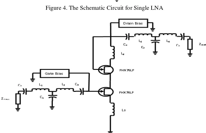
Figure 4 shows, the complete schematic of a single stage LNA and Figure 5 shows the completed schematic of a cascode LNA. A T-matching network was used to match the input impedance. Using Smith Chart matching techniques, the component values are shown in Table 3.To achieve the targeted overall gain of 35dB, it was decided to design cascode and cascaded technique.
Figure 4. The Schematic Circuit for Single LNA
Table 3. LNA parameters Items Components of Matching
Cascode LNA Single LNA
L1 6.14 nH 3.661 nH L2 2.4 nH 0.8799 nH L3 1.55 nH 3.60 nH
L4 1.62 nH 0.88 nH C1 0.315 pF 0.5 pF C2 429.9fF
4. Simulation Result
Table 4 shows the s-parameters output for comparison of LNA. It is simulated using Advanced Design System (ADS). The simulation recorded that the amplifier gain S21 is 36.3dB.The input insertion loss S11 was
-21.1dB, overall noise figure (NF) is 1.2dB and the output insertion loss S22 is -27.7dB.The reflection loss S12 is
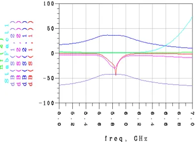
-42.5dB. These values were within the design specification and were accepted. The output S-parameter are shown in figure 6a, 6b and 6c
Table 4: Comparison of output LNA
S-Parameters (dB) S11 S12 S21 S22 NF (k)
Single LNA -12.8 -20.2 17.0 -27.9 0.76 1.02 Cascode LNA -18.9 -22.1 19.5 -20.0 1.2 1.02
Cascode and
Cascaded LNA -21.1 -42.5 36.3 -27.7 1.20 1.26
Figure 6a: S-parameters for single LNA
Figure 6b: S-parametersfor single cascode Figure 6c: S-parametersfor cascode and cascaded
5. Measurement
Referring to the measurement setup shown in Figure 7, the S parameter of the amplifier; whereas S11, S12, S21
and S22 were measured using the network analyzer. The gain of the amplifier was measured using the setup in Figure
8. The noise figure values and 3dB bandwidth were obtained from setup in Figure 9. Before all measurement is recorded, a standard procedure of calibration was followed to ensure that the measurement tools were calibrated.
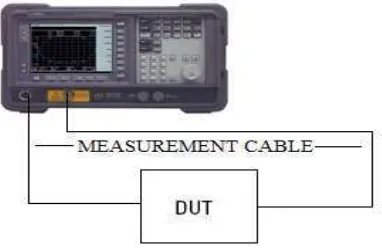
Figure 7. Setup for device under test S Measurement using Network Analyzer
Figure 8. Frequency response measurement setup for device under test.
Figure 9: Measurement setup for device under test for Noise Figure
Table 5: S-parameters measured
S Parameters Targeted Measured
Input Reflection S11 dB <-10 dB -11.4
Return Loss S12 dB <-10 dB -39.1
Forward transfer S21 dB >35 dB 36.8
Output ReflectionS22 dB <-10 dB -12.3
NF dB * <3 dB 1.3
6. Result
The result for LNA RF front-end module is presented in Table 5. From the tabulated values, the S11
parameter measured is 11.4 dB. This is -1.4 dB less than targeted which is better and acceptable. S22 measured is
-12.3 dB which is less than targeted and acceptable. The return loss required S12 obtained was less than -39 dB. The
related measured gain S21 for the LNA amplifier is 36.8 dB measured using the setup in Figure 6. The noise figure
values obtained from setup in Figure 8 is 1.37 dB which complied with the targeted value of less 3 dB. The use of T lump reactive element and microstrip line matching technique at the input of the LNA contributes the best performance for the amplifier. This matching technique was used to provide high-loaded Q factor for better sensitivity and thus minimized the noise figure. The elements of T-network were realized in the form of lump reactive elements and microstrip line impedance. The 3 dB bandwidth for the amplifier is measured using setup Figure 7. The 3dB bandwidth obtained is 1.24 GHz compliant with targeted result of more than 1 GHz. The measured parameters for the LNA were also compliant with the equation (1) to (9) using MathCAD analysis.
7. Conclusion
A low noise amplifier has been simulated and developed successfully with IEEE standard 802.16 WiMAX. It is observed that the simulated and experiment results have not much different. It observed that the gain of the simulated analysis is 36.3 dB and the experimental value is 36.8 dB. It is important to take note when designing the amplifier to match the amplifier circuits. The 5.8GHz LNA has been developed successfully and the circuit cab contributed to the front end receiver at the described frequency. For better performance in gain of the amplifier, it can be achieved by increasing the number of stages to improve the gain and noise figure of the design. Higher gain would expand the coverage or communication distance.
References
[1] M.Ben Amor, M.Loulou, D.Pasquut, "A wideband CMOS LNA design for WiMAX application." IEEE Proceeding 2008.
[2] Ruey-Lue Wang, Shih-Chih Chen,Cheng-Lin Huang,Chien-Hsuan Lie,Yi-Shu Lin. "2-6GHz Current-reused LNA With Transformer-type Inductors." IEEE Proceeding 2008.
[3] Leon, Michael Angelo G.Lorenzo and Maria Theresa G.De. "Comparison of LNA Topology for Wimax Application in a Standard 90-nm CMOS Process." 12th International Conference on Computer Modelling and Simulation. 2010. pp-642-647.
[4] M.Pozar, David. Microwave and RF Wireless System. Third Avenue,N.Y.John Wiley & Sons,in, 2001. [5] Gonzalez, Guillermo. Microwave Transistor Amplifier. 1996.
[6] Othman A.R, Hamidon A.H,Ting J.T.H and Mustaffa M.F. "High Gain Cascaded Low Noise Amplifier Using T-Matching Network." 4th ISBC 2010.
[7] Weber, Wuezhan Wang and Robert. "Design of a CMOS Low Noise Amplifier (LNA) at 5.8GHz and its Sensitivity Analysis." 11th NASA Symposium 2003.
Bibliography of authors
Abu Bakar Ibrahim received the B.S degree in electrical engineering and master degree from University of Technology Malaysia in 1998 and 2000 respectively. Currently is working toward the Ph.D. degree in development of low noise amplifier front-end receiver for wireless application at the Universiti Teknikal Malaysia Melaka.
Email: [email protected]
Abdul Rani Othman received B.eng in electrical and Electronic from University of Strathclyde and master degree in electrical and electronic from University Technology of Malaysia. He received Ph.D. in RF front-end receiver for wireless application from University of Teknikal Malaysia Melaka and now he joined Universiti Teknikal Malaysia Melaka.
Mohd Nor Husain received B.S in electrical and Electronic Engineering from University of Strathclyde and master degree in electronic communication from University of Essex England. He received Ph.D. in optical and waveguide from University of Bath England and now he joined Universiti Teknikal Malaysia Melaka. Email:[email protected]