Othman A. R, Hamidon A. H, Abdul Wasli. C, Ting J. T. H, Mustaffa M. F
Faculty of Electronic And Computer EngineeringUniversiti Teknikal Malaysia Melaka. PO Box 1600, Hang Tuah Jaya
Melaka, Malaysia
Keywords: Amplifier, Low Noise Amplifier, Radio
Frequency. Microstrip
Abstract
This project presents a design of high gain cascaded low noise amplifier (LNA), which operates at 5.8 GHz frequency for WiMAX application. The LNA designed used T matching network consist of lump reactive elements and microstrip at the input and output impedance. A cascaded LNA is developed in this project contributes a high gain of 36.8 dB with overall noise figure of 1.3 dB. The overall measured bandwidth measures is 1.240 GHz with S parameters S11, S12 and S22 measured are -11.4dB, -39.1dB
and -12.3dB respectively. The input sensitivity of the LNA is -80dBm which compliant with the IEEE 802.16 WiMAX application. The LNA used FET transistor FX 76 LP from Eudina Inc.
1 Introduction
The first stage of a receiver is typically a low noise amplifier (LNA), whose main function is to provide enough gain to overcome the noise of subsequent stages. Many researchers have been done in CMOS LNA area from 900 MHz to 9 GHz [1-4]. In the literature there are many LNA work designed in GaAs and bipolar technology [5-8]. In this paper a low voltage, low power and wideband Pseudomorphic High Electron Mobility Transistor (PHEMT) LNA at 5.8 GHz is designed and simulated using Ansoft Designer and ADS 2000A. As a design tool sensitivity analysis gives a measure of sensitivity for a LNA circuit performance due to change the active element to be PHEMT and assisting the designer in choosing adequate circuit elements tolerances [9]. Such sensitivity analysis of LNA is very beneficial for making appropriate design trade-off. Four LNA designed Using PHEMT with two operation
condition. The first two LNA is designed with the same parameters published in [1]. The second Two LNA is optimized to achieve a minimum noise figure with maximum gain available.
The progress of wireless communication services has increased the need for LNA designed which has higher capability in providing higher gains, better input sensitivity and minimize noise level. It is desirable to combine two or more standards in one mobile unit for overall capacity enlargement, higher flexibility and roaming capability as well as backward compatibility. Moreover multi standard RF receiver will allow access to different system providing various services. These are the cause of the investigation to increase the bandwidth of the systems for band multi-mode operation.
In WiMAX system, LNA designed for receiver system are breaking the bonds of wired connections in separated buildings to be connected in the area that the wired bridge is impossible to be deployed and installed. WiMAX wireless technology can be more economical and efficient than installing wired networks. With the current technology of Orthogonal Frequency Division Multiplexing (OFDM) adopted in IEEE 802.16 WiMAX standard, the system can provide high data rate up to 70 Mbps [2]. The RF receiver in WiMAX system plays a paramount role for converting baseband signal from the RF signal so that the system can be communicating wirelessly. Therefore, the performance of the WiMAX system also relies on the RF front end receiver system such as LNA where it must be well designed to minimize the noise level (or distortions) in the system.[3]. The approach taken in designing the amplifiers involves a series of chronological steps. No design is complete without some desired goals. The design specifications for the low noise amplifier were shown in Table 1.1:
High Gain Cascaded Low Noise Amplifier Using T Matching
Network
Parameter LNA
Gain dB > 35
Frequency 5.8 GHz
NF dB < 3
Matching Technique Microstrip and lump reactive element
VSWR 1.5
Bandwidth MHz >1000 (5.8 GHz Centre) Input sensitivity - 80 dBm (WiMAX)
Table 1.1: Design specifications for LNA
With refer to Table 1.1 the gain targeted for the LNA is more than 35 dB. This gain is necessary to amplify week signals and separated from the noise. The amplifier will maintain noise figure less than 3 dB and provide bandwidth of 1000 MHz. The input sensitivity for the LNA is set at -80dBm compliant with the standard WiMAX application.
2 Theoretical Description
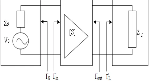
Basically, for a design of amplifier, the input and output matching network are designed to achieve the required stability, small signal gain, and bandwidth [4]. Super high frequency amplifier is a typical active circuit used to amplify the amplitude of RF signal. Basic concept and consideration in design of super high frequency amplifier is presented below. For the LNA design the formulae and equation were refer to [1]. Figure 2.1 shows a typical single-stage amplifier including input/output matching networks.
Figure 2.1: Typical amplifier designed
In short, basic concept of high frequency amplifier design is to match input/output of a transistor for high frequencies having S parameters [S] frequency characteristics at a specific DC-bias point with source impedance and load impedance. I/O matching circuit is essential to reduce unwanted reflection of signal and to improve efficiency of
transmission from source to load. The targeted specification amplifier is shown in Table 1.1.
2.1 Power Gain
Several power gains are defined to understand operation of super high frequency amplifier, as shown in Figure 2.2, power gains of 2 port circuit network with power impedance or load impedance at power amplifier represented with scattering coefficient are classified into Operating Power Gain, Transducer Power Gain and Available Power Gain.[4],[5]
Figure 2.2: I/O circuit of 2-port network
2.2 Operating Power Gain
Operating power gain is the ratio of power (PL) delivered to the load (ZL) to power (Pin) supplied to 2 port network. Power delivered to the load is the difference between the power reflected at the output port and the input power, and power supplied to 2-port network is the difference between the input power at the input port and the reflected power. Therefore, Operating Power Gain is represented by
)
1
(
|
1
|
|
|
1
|
|
|
|
1
1
supplied
2 22
2 2
21 2
L L
in in
L P
S
S
P
P
amplifier
the
to
power
load
the
to
delivered
Power
G
Γ
−
−
Γ
Γ
−
=
=
=
2.3 Transducer Power Gain
Transducer Power Gain is the ratio of
P
avs, maximum power available from source toP
L, power delivered to the load. As maximum power is obtained when input impedance of circuit network is equal to conjugate complex number of power impedance, ifΓ
in=Γ
s , transducer power gain is represented by)
2
(
|
)
(
)
1
)(
1
(
|
)
|
|
1
)(
|
|
1
(
|
|
supplied
2 21 12 22 11 2 2 2 21 L S L S L S in L PS
S
S
S
S
P
P
amplifier
the
to
power
load
the
to
delivered
Power
G
Γ
Γ
−
Γ
−
Γ
−
−
Γ
−
Γ
=
=
=
Where,
Γ
L indicates load reflection coefficient.2.4 Available Power Gain
Available Power Gain,
G
A is the ratio ofP
avs , power available from the source, toP
avn, power available from 2-port network, that is,avs avn A
P
P
G
=
. Power gain isP
avnwhen
Γ
in=Γ
*
s. Therefore Available Power Gain is given by:)
3
(
|
1
|
1
|
|
|
1
|
|
|
1
supplied
2 22 2 21 2 11 2 L S S avs avn AS
S
S
P
P
amplifier
the
to
power
load
the
to
delivered
Power
G
Γ
−
Γ
−
−
Γ
=
=
=
That is, the above formula indicates power gain when input and output are matched.
2.5 Noise Figure
Signals and noises applied to the input port of amplifier are amplified by the gain of the amplifier and noise of amplifier itself is added to the output. Therefore, SNR (Signal to Noise Ratio) of the output port is smaller than that of the input port. The ratio of SNR of input port to that of output port is referred to as noise figure and is larger than 1 dB. Typically, noise figure of 2-port transistor has a minimum value at the specified admittance given by formula:
)
4
(
|
|
2min s opt S
N
Y
Y
G
R
F
F
=
+
−
For low noise transistors, manufactures usually provide
opt N
Y
R
F
min,
,
by frequencies. N defined by formula for desired noise figure:)
5
(
|
1
|
/
4
|
|
1
|
|
2 0 min 2 2 opt N S opt sZ
R
F
F
N
=
−
+
Γ
Γ
−
Γ
−
Γ
=
2.6 Design LNA
From equation (1) to (5), the related power gain and noise figure for single stage LNA are calculated. By using ADS 2005A, the noise figure circle is outside the unit circle and the VSWR recorded is 2.179. From simulation, it was recorded that the amplifier gain S21 is 17.23 dB. The input
insertion loss S11 is -6.28dB and the output insertion loss S22
is -7.60dB. The reflected loss S12 is -20.18 dB and the noise
figure is 1.16 dB. These values were within the design specification and were accepted.
The overall performance of the low noise amplifier is determined by calculating the transducer gain GT, noise
figure F and the input and output standing wave ratios, VSWRIN and VSWROUT. The optimum,
Γ
optandΓ
L wereobtained as
Γ
opt = 17.354 +j 50.131 andL
Γ
= 79.913- j7.304. The calculated gain for the LNA was 19.3 dB, which correspond to a noise figure of 0.301 dB. The input matching loadΓ
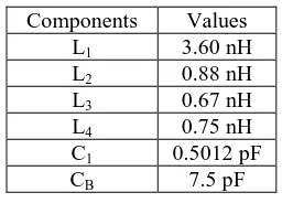
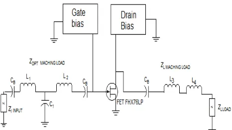
opt is required to provide high-loaded Q factor for better sensitivity. A T-network was used to match the input impedance. The elements of T-network can be realized in the form of lump reactive elements and microstrip line impedance. Using Smith Chart matching technique, the component values are shown in Table 2.1. The DC block capacitor is selected for the circuit and the value is recommended at least 10 times from the C1. For thisreason 7.5 pF capacitors are selected as bypass capacitors. With these components, the schematic circuit for single stage LNA is shown in Figure 2.3.
Components Values
L1 3.60 nH
L2 0.88 nH
L3 0.67 nH
L4 0.75 nH
C1 0.5012 pF
CB 7.5 pF
Figure 2.3: The schematic circuit for single stage amplifier To achieve the targeted overall gain of 35 dB, it was decided to design a cascaded amplifier using similar stages to double the LNA gain. The simulation of cascaded amplifier will be discussed in section below.
3 Simulation
The cascaded amplifier is then redrawn and simulated again using Ansoft Designer SV and the related frequency response and output gain is shown in Figure 3.1.
Figure 3.1: Cascaded LNA
Figure 3.2: Frequency Response versus Gain
The S parameters output is shown in Figure 3.2 , it is observed that the gain archive S21 is 36.80 dB at 5.8 GHz
frequency and the corresponding input insertion loss S11 is
-9.12 dB, reflection loss S12 is -39.13 dB and output insertion
loss S22 is -10.86 dB. The stability factor after matching
load is shown in Figure 3.3 and Figure 3.4. Figure 3.3 shows the stability circle lies inside Smith Chart diagram while Figure 3.4 shows the obtained stability factor k is 1 and VSWR observed is 1.49. These parameters are compliant with the targeted specifications of the amplifier for unconditional stable condition k is 1 and VSWR is targeted as 1.5. The noise figure output observed is 1.37 dB for the cascaded amplifier as shown in Figure 3.5.
Figure 3.4: Stability factor k for matched load
Figure 3.5: Noise Figure parameter for matched load
The simulated S parameters of the amplifier is tabulated in Table 3.1
Table 3.1: S Parameter Output and Targeted Parameters of Cascaded LNA
Figure 3.6: LNA Layout
This designed circuit is sent for fabrication and the LNA layout is shown in Figure 3.6
4 Measurement
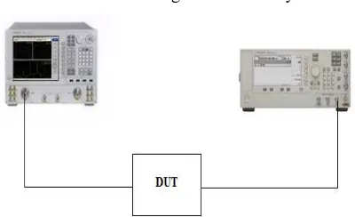
With refer once to measurement setup shown in Figure 4.1, the S parameter of the amplifier; whereas S11, S12, S21 and
S22 are measured using the network analyzer. The gain of
the amplifier is measured using the setup Figure 4.2. The noise figure values and 3 dB bandwidth are obtained from setup Figure 4.3. Before all measurement was recorded, a standard procedure of calibration was followed to ensure that the measurement tools were calibrated.
Figure 4.1: Measurement setup for device under test for S Measurement using Network Analyzer
Figure 4.2: Measurement setup for device under test for Frequency Response.
S Parameters LNA Simulated LNA Input reflection S11 dB -10 -9.12
Return Loss S12 dB -10 -39.13
Forward Transfer S21 dB 35 36.80
Output Reflection loss S22 dB -10 -10.86
Figure 4.3: Measurement setup for device under test for Noise Figure
5 Result
The result for LNA RF front-end module is presented in Table 5.1.
Table 5.1: S Parameter result for LNA
* Measured using noise figure analyzer in Telecom R&D.
From the tabulated values, the S11 parameter measured is
11.4 dB. This is -1.4 dB less than targeted which is better and acceptable. S22 measured is -12.3 dB which is less than
targeted and acceptable. The return loss required S12
obtained is less than -39 dB. The related measured gain S21
for the LNA amplifier is 36.8 dB measured using the setup Figure 4.3. The noise figure values obtained from setup Figure 4.4 is 1.37 dB which complied with the targeted value of less 3 dB. The use of T lump reactive element and microstrip line matching technique at the input of the LNA contributes the best performance for the amplifier. This matching technique was used to provide high-loaded Q factor for better sensitivity and thus minimized the noise figure [6]. The elements of T-network were realized in the form of lump reactive elements and microstrip line impedance. The 3 dB bandwidth for the amplifier is measured using setup Figure 4.3. The 3dB bandwidth obtained is 1.24 GHz compliant with targeted result of more
than 1 GHz. The measured parameters for the LNA were also compliant with the formulae (1) to (5) using MathCAD analysis.
6 Conclusion
A low noise amplifier has been simulated and developed successfully with IEEE standard 802.16 WiMAX. It is observed that the simulated and experiment results have not much different. It observed that the gain of the simulated analysis is 34.22 dB and the experimental value is 36.8 dB. It is important to take note when designing the amplifier to match the amplifier circuits. The 5.8GHz LNA has been developed successfully and the circuit cab contributed to the front end receiver at the described frequency. For better performance in gain of the amplifier, it can be achieved by increasing the number of stages to improve the gain and noise figure of the design. Higher gain will expand the coverage or communication distance.
Acknowledgement
The authors would like to thank UTeM which has financially sponsored this research project under short-term research grant.
References
[1] Xuezhen Wang and Robert Weber,”Design a CMOS Low Noise Amplifier (LNA) at 5.8 GHz and its sensitivity analysis”, 11th NASA Symbosium, 2003.
[2] Institute of Electrical and Electronic Engineering (IEEE). 1999,’IEEE Standard: Part 11, Wireless LAN Medium Access Control (MAC) and Physical Layer (PHY) specifications: High-speed Physical Layer in the 5 GHz Band. IEEE 802.11a.’
[3] Jui-Hung Yeh, Jyh-Cheng Chen, Chi-Chen Lee. Oct./Nov. 2003,’ WLAN standards’:. Potentials IEEE. . 22(4): pg16 – 22
[4] Man & Tel Co.Ltd,2006,MW-2000 Microwave Communication Trainer ,Manual Trainer
[5] David M. Pozar. 2001, ‘Microwave and RF Wireless System’. Third Avenue, N.Y.: John Wiley &Sons,In
[6] Bahl, I. & Bhartia, P. (2003). Microwave Solid State Circuit Design, 2nd Edition, J Wiley, pp. 133-180.
S Parameters Targeted Measured Input Reflection S11 dB <-10 dB -11.4
Return Loss S12 dB <-10 dB -39.1
Forward transfer S21 dB >35 dB 36.8
Output ReflectionS22 dB <-10 dB -12.3
NF dB * <3 dB 1.3