ISSN: 2180 - 1843 Vol. 3 No. 2 July-December 2011
Design of LNA at 5.8GHz with Cascode and Cascaded Techniques Using T-Matching Network for WiMAX Applications
23
Abstract
This project presents a 5.8 GHz Low Noise Ampliier (LNA) design with cascode and cascaded techniques using T-matching network applicable for IEEE 802.16 standard. The ampliier uses the FHX76LP Low Noise SuperHEMT FET. The design simulation process is done by using the Advance Design System (ADS) sotware. The cascode and cascaded low noise ampliier (LNA) produces a gain of 53.4dB and noise igure (NF) of 1.2dB. The input relection (S11) and output return loss (S22) are -24.3dB and -23.9dB respectively. The input sensitivity is complying with the IEEE 802.16 standards.
Keywords: Cascode and Cascade LNA, Radio Frequency, T -Matching Network
I. INTRODUCTION
The number of systems that use radio frequencies links is increasing rapidly. At the same time, the number of standards for such systems is increasing very quickly as well. To make this possible the number of frequency band dedicated for wireless communication has also increased [1]. WiMAX, which is short for Worldwide Interoperability for Microwave Access, is a novel wireless communication technology. It is an atractive technology due to the high transmiting speed (up to 70Mbps) and long transmiting distance (up to 30 mile). The system is based on the IEEE 802.16 standards and uses several bands (2.3-2.7 GHz, 3.4-3.6 GHz and 5.1-5.8GHz) to transmit data. The design of the front-end low noise ampliier (LNA) is one of the challenges in Radio Frequency (RF)
DesIgN Of LNA AT 5.8gHz wITH CAsCODe AND CAsCADeD
TeCHNIqUes UsINg T-MATCHINg NeTwORk fOR wIMAX
AppLICATIONs
A.B Ibrahim, Hussain M.N, Othman A.R, Johal M.s
Faculty of Electronic and Computer Engineering
Universiti Teknikal Malaysia Melaka
Email: [email protected], [email protected]
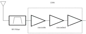
receivers, which needs to provide good input impedance match, enough power gain and low Noise Figure (NF) within the required band [2]. Many high gain ampliier topologies have been proposed as a way to satisfy the requirement for low power dissipation as well as good performances. The cascode with cascaded techniques produced, results in a higher bandwidth and gain, due to the increase in the output impedance, as well as beter isolation between the input and output ports [3-7]. The overall low noise ampliier should introduce a higher gain of 50 dB compared to reported [9]. It is by taking into consideration the extension of communication distance up to 50 km [10]. In this work, low noise ampliier with cascode and cascaded techniques (3-stage) is proposed a shown in Figure 1. NA)
. are is
Figure 1: Proposed for Cascode and Cascaded LNA
ISSN: 2180 - 1843 Vol. 3 No. 2 July-December 2011 Journal of Telecommunication, Electronic and Computer Engineering
24
design of super high frequency ampliier is presented in this paper.
of higher
tput
d Figure 2: Typical ampliier designedFigure 2: Typical amplifier designed
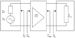
The LNA design formula and equation were referred to [4]. Figure 2, shows a typical single-stage ampliier including input/output matching networks. The basic concept of high frequency ampliier design is to match input/output of a transistor at high frequencies using S-parameters frequency characteristics at a speciic DC-bias point with source impedance and load impedance. Input/ output matching circuit is essential to reduce the unwanted relection of signal and to improve eiciency of the transmission from source to load [4-5].
A. power gain
Several power gains were deined in order to understand operation of super high frequency ampliier, as shown in Figure 2, power gains of 2-port circuit network with power impedance or load impedance at power ampliier represented with scatering coeicient are classiied into Operating Power Gain, Transducer Power Gain and Available
Power Gain [4-5]. − Γ − Γ − ΓΓ
Figure 3: I/O circuit of 2-port network
Operating power gain is the ratio of power (PL) delivered to the load (ZL) to power (Pin ) supplied to 2 port network. Power delivered to the load is the
diference between the power relected at the output port and the input power, and power supplied to 2-port network is the diference between the input power at the input port and the relected power. Therefore, Operating Power Gain is represented by
Γ
Where,
Γ
in indicates relection coeicient of load at the input port of 2-port networkand
Γ
s is relection coeicient of powersupplied to the input port.
C. Transducer power gain
Transducer Power Gain is the ratio of
P
avs , maximum power available from sourceto
P
L , power delivered to the load. As maximum power is obtained when input impedance of circuit network is equal to conjugate complex number of powerimpedance, if
Γ
in =Γ
s, transducerpower gain is represented by
2 gain is represented by
(2)
where, Γ indicates load reflection coefficient.
=
D. Available power gain
Available Power Gain
G
A is the ratio ofavs
P
, power available from the source,to
P
avn , power available from 2-portISSN: 2180 - 1843 Vol. 3 No. 2 July-December 2011
Design of LNA at 5.8GHz with Cascode and Cascaded Techniques Using T-Matching Network for WiMAX Applications
25
avn
P when Γin = Γ*s. Therefore Available Power Gain is given by:
Γ
That is, the above formula indicates power gain when input and output are matched [5].
e. Noise figure
Signals and noises applied to the input port of ampliier were ampliied by the gain of the ampliier and noise of ampliier itself is added to the output. Therefore, SNR (Signal to Noise Ratio) of the output port is smaller than that of the input port. The ratio of SNR of input port to that of output port is referred to as noise igure and is larger than 1 dB. Typically, noise igure of 2-port transistor has a minimum value at the speciied admitance given by formula:
For low noise transistors, manufactures
usually provide Fmin,RN,Yopt by frequencies. N deined by formula for desired noise igure:
− + =
F. Condition for Matching
Γ
f. Condition for Matching
The scatering coeicients of transistor were determined. The only lexibility permited to the designer is the input/ output matching circuit. The input circuit should match to the source and the output circuit should match to the load in order to deliver maximum power to the load. Ater stability of active device is determined, input/output matching
circuits should be designed so that relection coeicient of each port can be correlated with conjugate complex number as given below [6]:
− The noise figure of the first stage of the receiv noise figure of the whole system. To get
Γ
e receiver overrules
Γ whole system. To get minimum noise igure using transistor, power relection coeicient should match with Γopt and load relection coeicient should match
with *
ISSN: 2180 - 1843 Vol. 3 No. 2 July-December 2011 Journal of Telecommunication, Electronic and Computer Engineering
26 −
+ =
o . t n njugate
(6)
)
Γ Γ
Γ Γ
⎟⎟⎠ ⎞ ⎜⎜⎝
⎛
Γ
− Γ
+ = Γ = Γ
Γ Γ
Γ Γ
Γ Γ
Γ
Γ
− Γ
+ = Γ = Γ
Γ
− Γ
+ = Γ = Γ
Γ + − = Γ −
Γ − Γ =
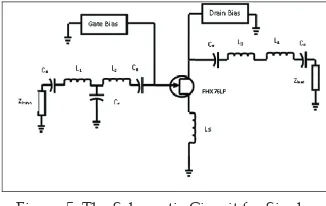
Figure 4: The Schematic Circuit for Cascode LNA
Table I: Components of Matching
− + =
Γ ld
Γ
Γ Γ (8)
⎟⎟⎠ ⎞ ⎜⎜⎝
⎛
Γ
− Γ
+ = Γ =
Γ (9)
Γ Γ
Γ Γ
Γ Γ
Γ
Items Components of Matching Cascode LNA Single LNA
L1 6.14 nH 3.661 nH
L2 2.4 nH 0.8799 nH
L3 1.55 nH 3.60 nH
L4 1.62 nH 0.88 nH
C1 0.315 pF 0.5 pF
C2 429.9fF
Γ
− Γ
+ = Γ = Γ
Γ
− Γ
+ = Γ = Γ
Γ + − = Γ −
Γ − Γ =
The input matching load is required to provide high-loaded Q factor for beter sensitivity. Several types of matching techniques had been tested for input matching. The criteria that is taken into consideration for choosing the most suitable matching network include low noise igure, high gain and high sensitivity.
Γ
Γ Figure 5: The Schematic Circuit for Single
LNA
Regarding the impedance of L
à is real, suitable matching impedance for the load is by using a quarter-wave transformer[8] Theoretically, the other types of matching techniques can be also applied on matching the
L
à . However, all of the
techniques require the usage of capacitor. From simulation, as we ixed the capacitance to the value witch available on market, it is not possible to match the load. An adjustable capacitor can be used to solve this problem; however, due to the higher cost of adjustable capacitor, it is not in our consideration. Thus, the best matching techniques is the wave transformer. The quarter-wave transformer converts the complex impedance into real impedance.
IV. sIMULATION ResULTs
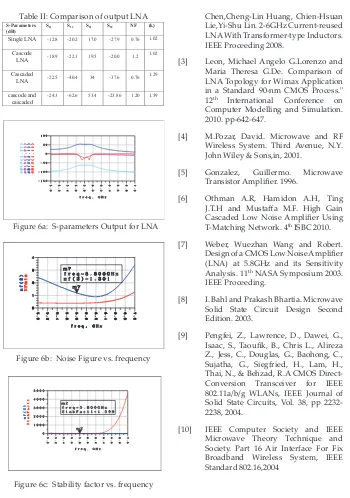
Table II shows the s-parameters output for comparison of LNA. It is simulated using Advanced Design System (ADS). The simulation recorded that the ampliier gain S21 is 53.4dB.The input insertion loss S11 is -24.3dB, overall noise igure (NF) is 1.2dB and the output insertion loss S22 is -23.9dB.The relection loss S12 is -62.6dB. These values were within the design speciication and were accepted. The output S-parameter (graphs) shows in igure consistence 6a, 6b and 6c.
V. CONCLUsION
ISSN: 2180 - 1843 Vol. 3 No. 2 July-December 2011
Design of LNA at 5.8GHz with Cascode and Cascaded Techniques Using T-Matching Network for WiMAX Applications
27 Table II: Comparison of output LNA
Γ
Γ
S-Parameters (dB)
S11 S12 S21 S22 NF (k)
Single LNA -12.8 -20.2 17.0 -27.9 0.76 1.02
Cascode
LNA -18.9 -22.1 19.5 -20.0 1.2
1.02
Cascaded
LNA -22.5 -40.4 34 -37.6 0.76
1.29
cascode and cascaded
-24.3 -62.6 53.4 -23.86 1.20 1.59
Γ e
Γ . f d the capacitance to
er cost of s,
Figure 6a: S-parameters Output for LNA Γ
Γ
all
d.
Figure 6b: Noise Figure vs. frequency
Figure 6c: Stability factor vs. frequency
RefeReNCes
[1] M. Amor, M. Loulou, and D.Pasquut. A wideband CMOS LNA design for WiMAX Application. IEEE Proceeding 2008.
[2] Ruey-Lue Wang, Shih-Chih
Chen,Cheng-Lin Huang, Chien-Hsuan Lie,Yi-Shu Lin. 2-6GHz Current-reused LNA With Transformer-type Inductors. IEEE Proceeding 2008.
[3] Leon, Michael Angelo G.Lorenzo and Maria Theresa G.De. Comparison of LNA Topology for Wimax Application in a Standard 90-nm CMOS Process." 12th International Conference on Computer Modelling and Simulation. 2010. pp-642-647.
[4] M.Pozar, David. Microwave and RF Wireless System. Third Avenue, N.Y. John Wiley & Sons,in, 2001.
[5] Gonzalez, Guillermo. Microwave Transistor Ampliier. 1996.
[6] Othman A.R, Hamidon A.H, Ting J.T.H and Mustafa M.F. High Gain Cascaded Low Noise Ampliier Using T-Matching Network. 4th ISBC 2010. [7] Weber, Wuezhan Wang and Robert.
Design of a CMOS Low Noise Ampliier (LNA) at 5.8GHz and its Sensitivity Analysis. 11th NASA Symposium 2003. IEEE Proceeding.
[8] I. Bahl and Prakash Bhartia. Microwave Solid State Circuit Design Second Edition. 2003.
[9] Pengfei, Z., Lawrence, D., Dawei, G., Isaac, S., Taouik, B., Chris L., Alireza Z., Jess, C., Douglas, G., Baohong, C., Sujatha, G., Siegfried, H., Lam, H., Thai, N., & Behzad, R.A CMOS Direct-Conversion Transceiver for IEEE 802.11a/b/g WLANs, IEEE Journal of Solid State Circuits, Vol. 38, pp 2232-2238, 2004.