Low Noise Figure of Cascaded LNA at 5.8GHz
Using T-Matching Network for WiMAX
Applications
Othman A.R, Ibrahim A.B, Husain M.N, Hamidon A.H, Hamidon Jsam
Abstract: This project presents the low Noise Figure (NF) cascaded Low Noise Amplifier (LNA) at 5.8GHz using T-matching network applicable for WiMAX application. The amplifier used FHX76LP Low Noise SuperHEMT FET. The LNA designed used T-matching network consisting of lump reactive element at the input and the output terminal. The cascaded LNA produced noise figure of 1.3 dB and forward gain of 36.8 dB. The input reflection (S11) and output return loss (S22) are -12.4 dB and -12.3 dB respectively. The bandwidth of the amplifier is more than 1.24 GHz. The input sensitivity is compliant with the IEEE 802.16 standards.
Keyword: Cascade LNA, Radio Frequency, T -Matching Network
I.INTRODUCTION
Today telecommunications industry continues to implement new technologies in an effort to provide high bandwidth, high-speed data transmission capabilities to the consumer. A combination of sophisticated wire line, fiber-optic and wireless technologies will most likely be deployed by this industry to satisfy consumer demand [1]. WiMAX, which is short for Worldwide Interoperability for Microwave Access, is a novel wireless communication technology. It is an attractive technology due to the high transmitting speed (up to 70Mbps) and long transmitting distance (up to 30 mile). The system bases on IEEE 802.16 standards and uses several bands (2.3-2.7 GHz, 3.4-3.6 GHz and 5.1-5.8GHz) to transmit data. The design of the front-end low noise amplifier (LNA) is one of the challenges in radio frequency (RF) receivers, which needs to provide good input impedance match, enough power gain and low noise figure (NF) within the required band [2].Many high gain amplifier topologies have been proposed as a way to satisfy the requirement for low noise figure (NF) as well as good performances. One of the techniques is cascading. Using this technique produces results of higher gain, due to the
increase in the output impedance, as well as better isolation between the input and output ports[3],[4]. Most of the single stage LNA device in the review produced around 2-3 dB noise figure (NF).
II. THEORETICAL
Noise Figure (NF) is a figure of merit quantitatively specifying how noisy a component or system is. The noise figure of a system depends on a number of factors such as losses in the circuit, the solid-state devices, bias applied and amplification. The noise factor of a two-port network is defined as [4]:
(2.1)
Where, SNR is signal noise ratio, Si is input signal, So is output signal, Ni is input noise, and No is output noise. The noise figure is simply the noise factor converted in decibel notation. Figure 1 shows the two-port network with a gain (or loss) G. we have
(2.2)
Figure 1: The Two-Port Network
Note that No≠ GNi; instead, the output noise No≠ GN+ noise generated by the network. The noise added by the network
(2.3)
(decibels). The noise component should be independent of the input noise. It is based on a standard input noise source Ni at room temperature in a bandwidth B, where:
(2.6)
Figure 2: Cascaded Circuit with n Network
The overall noise figure F is:
(2.8)
Equation 2.5 allows for the calculation of the noise figure of a general cascaded system. From eq. (2.8), it is clear that the gain and noise figure in the first stage are critical in achieving a low overall noise figure. It is very desirable to have a low noise figure and high gain in the first stage. To use Equation (2.8), all F’s and G’s are in ratio. For a passive component with loss L in ratio, we will have G = 1/L and F = L.
Note that, F=F1 due to the high gain in the first stage. The first-stage amplifier noise figure dominates the overall noise figure. One would like to select the first RF amplifier with a low noise figure and a high gain to ensure the low noise figure for the overall system.
The equivalent noise temperature is defined as
(2.9) Where T0=290K (room temperature) and F in ratio; therefore
(2.10)
For a cascaded circuit shown as Figure 3, equation (2.8) can be rewritten as
(2.11)
Where, Te is the overall equivalent noise temperature in Kelvin.
Figure 3: Noise Temperature for a Cascaded Circuit The noise temperature is useful for noise factor calculations involving an antenna for example, if an antenna noise temperature is TA, the overall system noise including the antenna is
(2.12) Where, Te is overall cascaded circuit noise temperature. As pointed out earlier the antenna noise temperature is approximately equal to 290K for an antenna pointing to earth. The antenna noise temperature could be very low (a few Kelvin) for an antenna pointing to the sky [4].
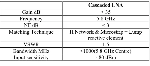
The design specifications for the cascaded LNA were shown in Table I:
Table I: Design Specification for LNA
III. LNA CIRCUIT DESIGN
The Cascaded LNA was design with advanced Design System (ADS 2008) with 2 Volts (VDS) and 10mA of bias current was supply. The overall performance of the low noise amplifier is determined by calculating the transducer gain GT, noise figure F and the input and output standing wave ratios,
Matching Technique Π Network & Microstrip + Lump reactive element
VSWR 1.5
The calculated gain for the LNA was 17 dB, which correspond to a noise figure of 0.301 dB. The input matching load
Γ
opt is required to provide high-loaded Q factor for better sensitivity. A T-network was used to match the input impedance. The elements of T-network can be realized in the form of lump reactive elements and microstrip line impedance. For the output impedance ZL, since the impedance is real, suitable matching for the load is by using a quarter-wave transformer [6], [8].The quarter-wave transformers convert the complex impedance into real impedance.Using Smith Chart matching technique, the component values are shown in Table II. The DC block capacitor was selected for the circuit and the value is recommended at least 10 times from the C1. For this reason 7.5 pF capacitors are selected as bypass capacitors. With these components, the schematic circuit for single stage LNA is shown in Figure 4. From equation (2.1) to (2.12), the related noise figure and gain of the amplifier were calculated. By using ADS 2008, the noise figure circle was obtained in the unit circle and the VSWR recorded was 2.179.
Figure 4: Single Stage LNA
Table II: LNA Parameters
Figure 5 shows the cascaded amplifier, this is realized from two single stages amplifiers. To achieve the targeted overall gain of 35 dB, it was decided to design a cascaded amplifier using similar stages to double the LNA gain. The components of matching are similar with single LNA but the L4=0.67nH, L5=0.88nH and C2=0.5pF was inserted. It is call inter-stage matching network.
Figure 5: Cascaded LNA
IV. SIMULATION RESULT
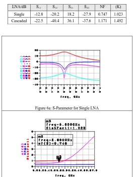
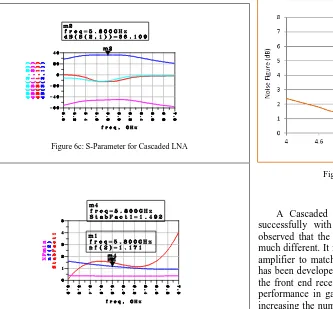
The simulated cascaded amplifiers results are shown in Table III. These values were within the design specification and were accepted. The graph outputs S-parameter are shown in Figure 6a, 6b, 6c and 6d.
Table III: S-Parameter Results for LNA
LNA/dB S11 S12 S21 S22 NF (K)
Single -12.8 -20.2 18.2 -27.9 0.747 1.023
Cascaded -22.5 -40.4 36.1 -37.6 1.171 1.492
Figure 6a: S-Parameter for Single LNA
Figure 6b: Noise Figure and Stability for Single LNA Components Values
L1 3.60 nH
L2 0.88 nH
L3 0.67 nH
L4 0.75 nH
C1 0.5 pF
Figure 6c: S-Parameter for Cascaded LNA
Figure 6d: Noise Figure and Stability for Cascaded LNA
V.MEASUREMENT
Before recording all measurements, a standard procedure of calibration is followed to ensure that the measurement tools were calibrated. Figure 7 shows the power output versus frequency for Cascaded amplifier. It is also tested for their frequency response. The signal generator output is set to -80 dBm according to IEEE 802.16 standard. The amplifier produced 36.8 dB and the output of the amplifier measured is -43.2 dBm with bandwidth more than 1.24 GHz. Figure 8 shows the noise figure measured for cascaded amplifier. The Noise Figure (NF) is measured using noise figure setup. It observed that the NF of the simulated analysis is 1.17 dB and the experimental value is 1.3 dB.
Figure 7: Power output vs Frequency (Cascaded)
Figure 8: Noise Figure (Cascaded)
VI. CONCLUSION
A Cascaded LNA has been simulated and developed successfully with IEEE standard 802.16 WiMAX. It is observed that the simulated and experiment results have not much different. It is important to take note when designing the amplifier to match the amplifier circuits. The 5.8GHz LNA has been developed successfully and the circuit contributed to the front end receiver at the described frequency. For better performance in gain of the amplifier, it can be achieved by increasing the number of stages to improve the gain and noise figure of the design. Higher gain would expand the coverage or communication distance.
REFERENCES
[1] Chia Wei chang and Zhi-Ming Lin. A 1V 14.6dB Gain LNA for WIMAX 2 – 6 GHz Application. IEEE Proceeding 2009.
[2] Ruey-Lue Wang, Shih-Chih Chen, Cheng-Lin Huang, Chien-Hsuan Lie,Yi-Shu Lin. "2-6 GHz Current-Reused LNA With Transformer-type Inductors." IEEE Proceeding 2008.
[3] Leon, Michael Angelo G.Lorenzo and Maria Theresa G.De. Comparison of LNA Topology for Wimax Application in a Standard 90-nm CMOS Process. 12th International Conference on Computer Modelling and Simulation. 2010. pp-642-647.
[4] Kai Chang, Inder Bahl, and Vijay Nair. Rf and Microwave Circuit for Wireless Systems 2009.
[5] Dorra Ayadi, Saul Rodriguez, Mourad Loulou, and Mohammad Ismail.System Level Design of Radio Frequency Receiver for IEEE 802.16 Standard. IEEE Proceeding 2009.
[6] I. Bahl and P.Bhartia. Microwave Solid State Circuit Design Second Edition 2003.
[7] Richard Chi-His Li. RF Circuit Design, 2009
[8] Inder J.Bahl. Fundamentals of RF and Microwave Transistor Amplifier 2009.