Abstract—This project presents the cascode and cascaded techniques LNA at 5.8GHz using T-matching network applicable for worldwide interoperability for microwave access (WIMAX) application. The amplifier uses FHX76LP Low Noise SuperHEMT FET. The LNA designed used T-matching network consisting of lump element reactive element at the input and the output terminal. The cascode and cascaded low noise amplifier (LNA) produced gain of 52.4dB and noise figure (NF) at 1.3dB. The input reflection (S11) and output return loss
(S22) are -19.71dB and -10.07dB respectively. The bandwidth of
the amplifier is more than 1.24GHz. The input sensitivity is compliant with the IEEE 802.16 standards.
Index Terms—Cascode-cascade LNA, radio frequency, T-matching network
I. INTRODUCTION
The modern wireless communication systems demand high data rate and high mobility performance during the last few years [1]. Worldwide interoperability for microwave access (WiMAX), which is short for Worldwide Interoperability for Microwave Access, is a novel wireless communication technology. It is an attractive technology due to the high transmitting speed (up to 70Mbps) and long transmitting distance (up to 30 mile). The system bases on IEEE 802.16 standards and uses several bands (2.3-2.7 GHz, 3.4-3.6 GHz and 5.1-5.8GHz) to transmit data. The design of the front-end low noise amplifier (LNA) is one of the challenges in radio frequency (RF) receivers, which needs to provide good input impedance match, enough power gain and low noise figure (NF) within the required band [2].
Many high gain amplifier topologies have been proposed as a way to satisfy the requirement for low power dissipation as well as good performances. The cascode with cascaded techniques to produces results in a higher bandwidth and gain, due to the increase in the output impedance, as well as better isolation between the input and output ports [3], [4]. Most of the single stage LNA device in the review could only around 20 dB gain. It was proposed that the low noise amplifier should have a gain of at least 30 dB [5]. By taking consideration the extension of communication distance of up to 50 km [5]. A budgeted high gain of LNA will ensure a good signal to noise separation for further amplification. For this gain of 50 dB, a cascode with cascaded amplifier is introduced for the low noise amplifier as shows in Fig. 1.
Manuscript received October 24, 2011; revised January 10, 2012. The authors are with Universiti Teknikal Malaysia Melaka, Malaysia (e-mail: [email protected]).
Fig. 1. Cascode and cascaded LNA
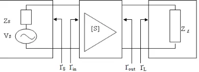
II. THEORETICAL ASPECTS
Basically, designing an amplifier, the input and output
matching network are consider to achieve the required stability, small signal gain, and bandwidth. Super high frequency amplifier is a typical active circuit used to amplify the amplitude of RF signal. Basic concept and consideration in design of super high frequency amplifier is presented in this paper. The LNA designed, the formula and equation were referred to [6]. Fig. 2, shows a typical single-stage amplifier including input/output matching networks.
Fig. 2. Typical amplifier design
The basic concept of high frequency amplifier design is to match input/output of a transistor at high frequencies using S-parameters frequency characteristics at a specific DC-bias point with source impedance and load impedance. Input/output matching circuit is essential to reduce the unwanted reflection of signal and to improve efficiency of the transmission from source to load [6], [7].
A. Power Gain
Several power gains were defined in order to understand operation of super high frequency amplifier, as shown in Fig. 3, power gains of 2-port circuit network with power impedance or load impedance at power amplifier represented with scattering coefficient are classified into Operating Power Gain, Transducer Power Gain and Available Power Gain [6], [7].
Fig. 3. I/O circuit of 2-port network
The Cascode and Cascaded Techniques LNA at 5.8GHz
Using T-Matching Network for WiMAX Applications
Abu Bakar Ibrahim, Abdul Rani Othman, Mohd Nor Husain, and Mohammad Syahrir Johal
B. Operating Power Gain
Operating power gain is the ratio of power (PL) delivered
to the load (ZL) to power (Pin) supplied to 2-port network.
Power delivered to the load is the difference between the power reflected at the output port and the input power, and power supplied to 2-port network is the difference between the input power at the input port and the reflected power. Therefore, Operating Power Gain is represented by
(1) where,
in indicates reflection coefficient of load at theinput port of 2-port network and
s is reflection coefficientof power supplied to the input port. C. Transducer Power Gain
Transducer Power Gain is the ratio of
P
avs, maximumpower available from source to
P
L, power delivered to the load. As maximum power is obtained when input impedance of circuit network is equal to conjugate complex number of power impedance, if
in=
s , transducer power gain iswhere,
L indicates load reflection coefficient. D. Available Power GainAvailable Power Gain,
G
Ais the ratio ofP
avs , poweravailable from the source, to
P
a vn, power available from 2- port network, that is, input and output are matched [7].E. Noise Figure
Signals and noises applied to the input port of amplifier were amplified by the gain of the amplifier and noise of amplifier itself is added to the output. Therefore, SNR (Signal to Noise Ratio) of the output port is smaller than that of the input port. The ratio of SNR of input port to that of output port is referred to as noise figure and is larger than 1
dB. Typically, noise figure of 2-port transistor has a minimum value at the specified admittance given by formula:
2
For low noise transistors, manufactures usually provide
opt
The scattering coefficients of transistor were determined. The only flexibility permitted to the designer is the input/output matching circuit. The input circuit should match to the source and the output circuit should match to the load in order to deliver maximum power to the load. After stability of active device is demand, input/output matching circuits should be designed so that reflection coefficient of each port is correlated with conjugate complex number as given below [8]: The noise figure of the first stage of the receiver overrules noise figure of the whole system. To get minimum noise figure using transistor, power reflection coefficient should match with
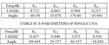
opt and load reflection coefficient should s-parameters were obtained from calculation and simulation using ADS. The S-parameter for each LNAs shows inTABLEII:S-PARAMETERS OFSINGLELNA
obtained as Γopt = 17.354 + j50.13 and ΓL = 79.913-j7.304
for single LNA. While, Γopt = 21 + j48.881 and ΓL =
79.913- j7.304 for cascode Low noise amplifier.
Fig. 4. The schematic circuit for cascode LNA
Fig. 4 shows, the complete schematic circuit of 5.8 GHz a cascode Low noise amplifier. The method employed here is inductive source degeneration. This degeneration inductor
enables more flexibility in matching the input stage to 50Ω. It
also influences the gain of LNA. Cascoding transistor is used to reduce the interaction of the gate-drain capacitance Cgd of
lower transistor. To increase flexibility and reduce the scope of possibilities the gate of cascoding transistor is assigned a maximum voltage by connecting it to VDD. The passive
elements in the input matching network are L1, L2 and
C1.While; the passive elements in the output matching
network are L3, L4 and C2. Combination of LS and L2 will
tune the input to the desired frequency [4]. The cascoding transistor consist of an inductor LD, it called peaking
structure to enhance gain and bandwidth [9]. This transistor also improves the reverse isolation and lowers miller effect [10]-[13].
Fig. 5 shows the completed schematic circuit of 5.8 GHz a single LNA. It also used source degeneration topology and an inductor Ls was inserted to provide the desired input resistance and to improve the stability of amplifier. The passive elements in the input matching network are L1, L2 and
C1. While; elements L3 and L4 are passive element in the
output network. For high gain amplification several amplifier are cascaded in series [11]. It can be designed as one unit or
all amplifiers are matched to 50Ω and connected in series. A
T-matching network is used to match the input impedance. Using Smith Chart matching techniques, the component values are shown in TABLE III. To achieve the targeted overall gain of 50dB; it is decided to design cascode and cascaded technique.
Fig. 5. The schematic circuit for single LNA
TABLEIII:LNAPARAMETERS
Items Components of Matching
Cascode LNA Single LNA
L1 6.14 nH 3.661 nH
L2 2.4 nH 0.8799 nH
L3 1.55 nH 3.60 nH
L4 1.62 nH 0.88 nH
C1 0.315 pF 0.5 pF
C2 429.9fF
IV. SIMULATION RESULT
TABLE IV shows the s-parameters output for comparison of LNA. It is simulated using Advanced Design System (ADS). The simulation recorded that the amplifier gain S21 is
53.4 dB. The input insertion loss S11 is -24.3dB, overall noise
figure (NF) is 1.2dB and the output insertion loss S22 is
-23.86dB.The reflection loss S12 is -62.6dB. These values
were within the design specification and were accepted. The outputs S-parameter are shown in Fig. 6a, 6b and 6c.
Fig. 6a. S-parameters for cascode LNA
Fig. 6b. S-parameters for cascaded
Fig. 6c. S-parameters for cascode and cascaded
TABLEIV:COMPARISON OF OUTPUT LNA
S-Parameters (dB)
S11 S12 S21 S22 NF (k)
Cascode LNA -18.9 -22.1 19.5 -20.0 1.2 1.02 Cascaded LNA -22.5 -40.4 34 -37.6 0.76 1.29
Cascode and
Cascaded LNA -24.3 -62.6 53.4 -23.86 1.20 1.59
S Parameters Targeted Measured
Input Reflection S11 dB <-10 dB -19.71
Return Loss S12 dB <-10 dB -65.72
Forward transfer S21 dB >50 dB 52.4
Output ReflectionS22 dB <-10 dB -10.07
NF dB <3 dB 1.3
BW MHz >1000 1240
V. MEASUREMENT
Referring to the measurement setup shown in Fig. 7, the S parameter of the amplifier; whereas S11, S12, S21 and S22 are
measured using the network analyzer. The gain of the amplifier is measured using the setup in Fig. 8. The noise figure values and 3dB bandwidth were obtained from the setup in Fig. 9. Before recording all measurement, a standard procedure of calibration is conducted to ensure that the measurement tools were calibrated.
Fig. 7. Setup for device under test s measurement using network analyzer
Fig. 8. Frequency response measurement setup for device under test.
Fig. 9. Measurement setup for device under test for noise figure
VI. RESULT
The result for LNA RF front-end module is presented in Table V. From the tabulated values, the S11 parameter
measured is -19.71 dB. This is -9.71 dB less than targeted value which is better and acceptable. S22 measured is -10.07
dB which is less than targeted and acceptable. The return loss
required S12 obtained is less than -65.72 dB. The related
measured gain S21 for the LNA amplifier is 52.4 dB measured
using the setup in Figure 6. The noise figure values obtained from setup in Figure 8 is 1.37 dB which complied with the targeted value of less 3 dB. The use of T lump reactive element and microstrip line matching technique at the input of the LNA contributes the best performance for the amplifier [9]. This matching technique was used to provide high-loaded Q factor for better sensitivity and thus minimized the noise figure. The elements of T-network were realized in the form of lump reactive elements and microstrip line impedance. The 3 dB bandwidth for the amplifier is measured using setup Fig. 7. The 3dB bandwidth obtained is 1.24 GHz compliant with targeted result of more than 1 GHz. The measured parameters for the LNA were also compliant with the equation (1) to (9) using MathCAD analysis.
VII. CONCLUSION
A low noise amplifier has been simulated and developed successfully with IEEE standard 802.16 WiMAX. It is observed that the simulated and experiment results have not much different. It observed that the gain of the simulated analysis is 53.4 dB and the experimental value is 52.4 dB. It is important to take note when designing the amplifier to match the amplifier circuits. The 5.8GHz LNA has been developed successfully and the circuit cab contributed to the front end receiver at the described frequency. For better performance in gain of the amplifier, it can be achieved by increasing the number of stages to improve the gain and noise figure of the design [11]. Higher gain would expand the coverage or communication distance.
REFERENCES
[1] C. W. Chang and Z.-M. Lin, “A 1V 14.6dB Gain LNA for WIMAX 2 - 6GHz Application,” IEEE Proceeding, 2009.
[2] R.-L. Wang, S.-C. Chen, C.-L. Huang, C.-H. Lie, and Y.-S. Lin,
“2-6GHz Current-Reused LNA With Transformer-type Inductors,” IEEE Proceeding, 2008.
[3] Leon, M. A. G. Lorenzo and M. T. G. De., “Comparison of LNA Topology for Wimax Application in a Standard 90-nm CMOS Process, ” 12th International Conference on Computer Modelling and Simulation, pp. 642-647, 2012.
[4] M. Pozar, David. Microwave and RF Wireless System. Third Avenue, N.Y.John Wiley & Sons, in 2001.
[5] Gonzalez, Guillermo. Microwave Transistor Amplifier. 1996. [6] A. R. Othman, A. H. Hamidon, J. T. H Ting, and M. F. Mustaffa, “High
Gain Cascaded Low Noise Amplifier Using T-Matching Network,” 4th ISBC 2010.
[7] Weber, W. Wang and Robert. “Design of a CMOS Low Noise Amplifier (LNA) at 5.8GHz and its Sensitivity Analysis,” 11th NASA Symposium 2003.
[8] IEEE Computer Society and IEEE Microwave “Theory Technique and Society. Part 16 Air Interface for Fix Broadband Wireless System,” IEEE Standard vol. 802, no. 16. 2004
[9] D. Ayadi, S. Rodriguez, M. Loulou, and M. Ismail, “System Level Design of Radio Frequency Receiver for IEEE 802.16 Standard,” IEEE Proceeding, 2009.
[10] R. C.-H. Li. “RF Circuit Design,”2009.
[11] I. J. Bahl. “Fundamentals of RF and Microwave Transistor Amplifier,” 2009.
[12] P. Bhartia and I. Bahl, “Microwave Solid State Circuit Design,” 2nd Edition, J Wiley, 2003.
Abu Bakar Ibrahim received the B.S degree in
electrical engineering and master degree from University of Technology Malaysia in 1998 and 2000 respectively. Currently is working toward the Ph.D. degree in development of low noise amplifier front-end receiver for wireless application at the Universiti Teknikal Malaysia Melaka. Email: [email protected]
Abdul Rani Othman received B.eng in electrical
and Electronic from University of Strathclyde and master degree in electrical and electronic from University Technology of Malaysia. He received Ph.D. in RF front-end receiver for wireless application from University of Teknikal Malaysia Melaka and now he joined Universiti Teknikal Malaysia Melaka. Email: [email protected]
Mohd Nor Husain received B.S in electrical and
Electronic Engineering from University of Strathclyde and master degree in electronic communication from University of Essex England. He received Ph.D. in optical and waveguide from University of Bath England and now he joined Universiti Teknikal Malaysia Melaka. Email:[email protected]
Mohammad Syahrir Johal received B.S in