ISSN: 2180 - 1843 Vol. 4 No. 1 January - June 2012
The Cascode LNA with RF Ampliier at 5.8GHz Using T-Matching Network for WiMAX Applications
15
Abstract
This paper presents the Cascode LNA with RF ampliier at 5.8GHz using T-matching network applicable for WIMAX application. The Cascode LNA uses FHX76LP Low Noise SuperHEMT FET and RF ampliier use EPA018A. The LNA designed used T-matching network consisting of lump element reactive element at the input and the output terminal. The Cascode LNA with RF ampliier produced gain of 36.4 dB and noise igure (NF) at 1.3dB. The input relection (S11) and output return loss (S22) are -12.4dB and -12.3 dB respectively. The bandwidth of the ampliier is more than 1.2GHz. The input sensitivity is compliant with the IEEE 802.16 standards.
Keywords: Cascode LNA, RFA, T -Matching Network.
I. INTRODUCTION
The increasing number of personal wireless communication systems demand for Radio Frequency (RF) front-end capable to handle diference standard speciication, i.e. WiMAX.[1]. WiMAX, which is short for Worldwide Interoperability for Microwave Access, is a novel wireless communication technology. It is an atractive technology due to the high transmiting speed (up to 70Mbps) and long transmiting distance (up to 30 mile). The system bases on IEEE 802.16 standards and uses several bands (2.3-2.7 GHz, 3.4-3.6 GHz and 5.1-5.8GHz) to transmit data. The design of the front-end low noise ampliier (LNA) is one of the challenges in radio frequency (RF) receivers, which needs to provide good input impedance match, enough power
The CasCODe LNa wITh RF ampLIFIeR aT 5.8Ghz UsING
T-maTChING NeTwORk FOR wImaX appLICaTIONs
Abu Bakar Ibrahim, Abdul Rani Othman, Mohd Nor Husain, Mohammad
Syahrir Johal, J. Sam Hamidon
Faculty of Electronic and Computer Engineering,
Universiti Teknikal Malaysia Melaka, Malaysia
Email: [email protected]
gain and low noise igure (NF) within the required band [2].Many high gain ampliier topologies have been proposed as a way to satisfy the requirement for low power dissipation as well as good performances. The Cascode with RF ampliier to produces results in a higher bandwidth and gain, due to the increase in the output impedance, as well as beter isolation between the input and output ports [3]. Most of the single stage LNA device in the review could only around 20 dB gain. It was proposed that the low noise ampliier should have a gain of at least 30 dB [8]. By taking consideration the extension of communication distance of up to 50 km [8]. A budgeted high gain of LNA will ensure a good signal to noise separation for further ampliication. For this gain of 30 dB, a Cascode LNA with RF ampliier is introduced. It is shows in Figure 1.
Figure 1: Cascode LNA and RFA
Figure 1: Cascode LNA and RFA
ISSN: 2180 - 1843 Vol. 4 No. 1 January - June 2012 Journal of Telecommunication, Electronic and Computer Engineering
16
is presented in this paper. The LNA designed, the formula and equation were referred to [4]. Figure 2, shows a typical single-stage ampliier including input/ output matching networks.
for novel attractive
bps) m .3-. The
of
eds Figure 2: Typical ampliier design
The basic concept of high frequency ampliier design is to match input/output of a transistor at high frequencies using S-parameters frequency characteristics at a speciic DC-bias point with source impedance and load impedance. Input/ output matching circuit is essential to reduce the unwanted relection of signal and to improve eiciency of the transmission from source to load [4],[5].
a. power Gain
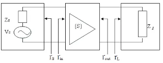
Several power gains were deined in order to understand operation of super high frequency ampliier, as shown in Figure 3, power gains of 2-port circuit network with power impedance or load impedance at power ampliier represented with scatering coeicient are classiied into Operating Power Gain, Transducer Power Gain and Available Power Gain [4],[5].
Γ
Figure 3: I/O circuit of 2-port network
Γ Figure 3: I/O circuit of 2-port network
B. Operating power Gain
Operating power gain is the ratio of power (PL) delivered to the load (ZL) to power (Pin) supplied to 2-port network. Power delivered to the load is the diference between the power relected at the output port and the input power, and power supplied to 2-port network is
the diference between the input power at the input port and the relected power. Therefore, Operating Power Gain is represented by
2 Where, Γ indicates reflection coefficient of l
Γ Where, Γin indicates relection coeicient of load at the input port of 2-port network and Γs is relection coeicient of power supplied to the input port.
C. Transducer power Gain
Transducer Power Gain is the ratio of Pavs, maximum power available from source to PL power delivered to the load. As maximum power is obtained when input impedance of circuit network is equal to conjugate complex number of power impedance, if Γin = Γs, transducer power gain is represented by
Γ
represented by
Where, ΓL indicates load reflection coefficie
= Γ
D. available power Gain
Available Power Gain, GA is the ratio of Pavs , power available from the source, to Pavn , power available from 2-port network, that is,. Power gain is Pavn when Γin = Γs. Therefore Available Power Gain is given by:
ISSN: 2180 - 1843 Vol. 4 No. 1 January - June 2012
The Cascode LNA with RF Ampliier at 5.8GHz Using T-Matching Network for WiMAX Applications
17
e. Noise Figure
Signals and noises applied to the input port of ampliier were ampliied by the gain of the ampliier and noise of ampliier itself is added to the output. Therefore, SNR (Signal to Noise Ratio) of the output port is smaller than that of the input port. The ratio of SNR of input port to that of output port is referred to as noise igure and is larger than 1 dB. Typically, noise igure of 2-port transistor has a minimum value at the speciied admitance given by formula:
For low noise transi
Γ
For low noise transistors, manufactures usually provide Fmin,RN,Yopt by
frequencies. N deined by formula for desired noise igure:
Γ
F. Condition for matching
The scatering coeicients of transistor were determined. The only lexibility permited to the designer is the input/ output matching circuit. The input circuit should match to the source and the output circuit should match to the load in order to deliver maximum power to the load. Ater stability of active device is demand, input/output matching circuits should be designed so that relection coeicient of each port is correlated with conjugate complex number as given below [6]:
Γ
correlated with conjugate complex
whole system. To get minimum noise igure using transistor, power relection
coeicient should match with Γopt and load relection coeicient should match with * the S-parameters were obtained from calculation and simulation using ADS 2008. The S-parameter for Cascode LNA is shows in Table 1.
Table 1 : S-Parameters of Cascode LNA
The overall performance of the low noise amplifier is
Γ Γ Γ Angle -86.54 33.878 178.66 -10.456
The overall performance of the low noise ampliier is determined by calculating the transducer gain GT, noise igure F and the input
and output standing wave ratios, VSWRIN and
VSWROUT. The optimum, Γopt and ΓL were
obtained as Γopt = 17.949 + j48.881 and ΓL =
79.913-j7.304 for single LNA. Γ Γ Γ
Γ
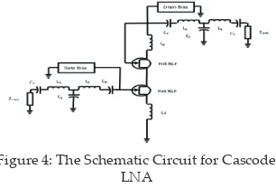
Figure 4: The Schematic Circuit for Cascode LNA
Γ Γ Γ
Γ
Π Ώ
Figure 4: The Schematic Circuit for Cascode LNA
ISSN: 2180 - 1843 Vol. 4 No. 1 January - June 2012 Journal of Telecommunication, Electronic and Computer Engineering
18
and C1.While; the passive elements in the output matching network are L3, L4 and C2. The load transistor consist of an inductor LD, it call peaking structure to enhance gain and bandwidth [9]. This transistor also improves the reverse isolation and lowers miller efect [10],[13].
Γ Γ Γ
Γ
Figure 5: The Schematic Circuit for RFA
Γ Γ Γ
Γ
Π Ώ
Figure 5: The Schematic Circuit for RFA
Figure 5 shows the completed schematic circuit of a RF ampliier with associated component and the 3 dB atenuator resistors. The RF ampliier was design based on [6] and [7]. Using theoretical design equation for the RFA, the equations are computed using Mathcad. The FET chosen for the design is EPA018A.The S-parameter given for the FET is shown in Table 2. These parameter were measured at VDD =2V and IDS= 10mA which sets the biasing for FET. This transistor biasing circuit is similar with the LNA ampliier
Table 2 : S-Parameters of RF Ampliier
re 8.
Γ Γ Γ
Γ
Gain, noise figure, input and output matching component
Γ Γ Γ
Γ
Π Ώ
Frequency/dB S11 S12 S21 S22
5.8 GHz 0.728 0.049 6.327 0.237 Angle -103.02 25.88 89.98 10.456
Gain, noise igure, input and output matching component were calculated and simulated using MathCAD and ADS 2008. Both calculated and simulated results were almost similar shows in Table 4. The calculated transducer power gain for matched condition was 17.3 dB. The input matching for optimum Γopt and ΓL were
obtained as Γopt= 12.662 +j 38.168 and ΓL= 79.97- j7.286. The noise igure calculated is 2.475 dB. The RF ampliier can also act as an isolator for the overall front-end system and a suitable Π-network with 50 Ώ load impedance was inserted at the input and output of the ampliier to provide 3 dB atenuation each for the network. The purpose of 3 dB atenuation is to isolate the system from the relected load power and to improve the return
loss of overall systems. The Cascode LNA and RF ampliier Matching component are shown in Table 3.
Table 3: Cascode LNA and RFA Matching parameters
Γ Γ Γ
Γ
GHz
Γ Γ Γ
Γ
Π Ώ
Components LNA(Values) RFA(Values) L1 6.14 nH 7.21nH
L2 2.4 nH 2.65nH
L3 1.55 nH 0.67nH
L4 1.62 nH 0.75nH
C1 0.315 pF 0.3pF
C2 429.9fF
IV. sImULaTION ResULT
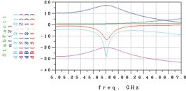
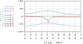
Table 4 is shows the S-parameters output for Cascode LNA, RF ampliier and Cascode LNA with RFM. It is simulated using Advanced Design System (ADS). The simulation recorded that the ampliier gain S21 is 36.1 dB. The input insertion loss S11 is -12.14dB, overall noise igure (NF) is 1.2dB and the output insertion loss S22 is -10.87 dB. The relection loss S12 is -45.47dB. These values were within the design speciication and were accepted. The outputs S-parameter are shown in igure 6a, 6b and 6c.
Γ Γ Γ
Γ
Γ Γ Γ
Γ
Π Ώ
Figure 6a: S-parameters for Cascode Figure 6a: S-parameters for Cascode
Figure 6b: S-parameters for RFA
Π Ώ
ISSN: 2180 - 1843 Vol. 4 No. 1 January - June 2012
The Cascode LNA with RF Ampliier at 5.8GHz Using T-Matching Network for WiMAX Applications
19
Figure 6c: S-parameters for Cascode with RFA
Π Ώ
Figure 6c: S-parameters for Cascode with RFA
Table 4: Comparison of output LNATable 4: Comparison of output LNA
Π Ώ
S-Parameters
(dB) S11 S12 S21 S22 NF
Cascode LNA -18.9 -22.1 19.5 -20.0 1.2 RF Amplifier -12.5 -21.5 17.3 -12.6 2.47 Cascode and
RFA -24.3 -62.6 36.1 -23.86 1.20
V. measURemeNT aND
aNaLYsIs
The result for Cascode LNA RF front-end was presented in Table 5.
Table 5: S Parameter result for Cascode LNATable 5: S Parameter result for Cascode LNA
S Parameters Targeted Measured
Input Reflection S11 dB <-10 dB -11.5
Return Loss S12 dB <-10 dB -27.3
Forward transfer S21 dB >17 dB 18.5
Output ReflectionS22 dB <-10 dB -12.3
NF dB * <3 dB 1.3 BW MHz >1000 1400
From the tabulated values, the S11 parameter measured is
Π Ώ
From the tabulated values, the S11 parameter measured is 11.5 dB. This is -1.5 dB less than targeted which is beter and acceptable. S22 measured is -12.3 dB which is less than targeted and acceptable. The return loss required S12 obtained was less than -27.3 dB. The related measured gain S21 for the LNA ampliier was 18.5 dB. The noise igure values obtained was 1.3 dB which complied with the targeted value of less 3 dB. The use of T lump reactive element and microstrip line matching technique at the input of the LNA contributes the best performance for the ampliier. This matching technique was used to provide high-loaded Q factor for beter sensitivity and thus minimized the noise igure. The elements of T-network were realized in the form of lump reactive elements and microstrip line impedance. The 3 dB bandwidth for the ampliier is measured
and the frequency response of LNA is shown in Figure 7. The 3dB bandwidth obtained was 1.4 GHz compliant with targeted result of more than 1 GHz.
Table 6: S-Parameters for RF Ampliier
S Parameters Targeted Measured
Input Reflection S11 dB <-10 -10.6 Return Loss S12 dB <-10 -31.8 Forward transfer S21 dB >15 15.6 Output ReflectionS22 dB <-10 -13.3 NF dB * <3 2.47
BW MHz 1000 1200
The RF amplifier measurement setup was similar to the
Π Ώ
The RF ampliier measurement setup was similar to the measurement set up for LNA. The results were shown in Table 6.
Figure 7: Power output vs Frequency GHz Cascode LNA
Π Ώ
Figure 7: Power output vs Frequency GHz Cascode LNA
ISSN: 2180 - 1843 Vol. 4 No. 1 January - June 2012 Journal of Telecommunication, Electronic and Computer Engineering
20
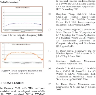
Both ampliiers were then cascaded and tested with 10dB atenuation set on the spectrum analyzer the output power versus frequency is shown in Figure 9. It was observed that the power output is -36.6 dBm and is expected if includes the total loss from cable and connector of 3 dB
The Front-end system designed consisted of a LNA with RFA were developed. The inal result for overall ampliier gain is 36.4 dB gains with noise igure of 1.3 dB. The total insertion loss is -25.5 dB. With injecting a -60 dBm signal and that atenuator setup of spectrum is 10 dB. For a wireless communication system such as WiMAX system, this RF front-end receiver will capable to provide a beter pipeline for the receiver with minimum noise igure and provide a high gain. This output is acceptable for further processing of the baseband system for IEEE 802.16 WiMAX standard.
Figure 8: Power output vs Frequency GHz RFA
Figure 9: Power output vs Frequency for Cascode LNA + RF Amp
Figure 9: Power output vs Frequency for Cascode LNA + RF Amp
VI. CONCLUsION
The Cascode LNA with RFA has been simulated and developed successfully with IEEE standard 802.16 WiMAX.
It is observed that the simulated and experiment results have not much diferent. It observed that the gain of the simulated analysis is 36.1 dB and the experimental value is 36.4 dB. It is important to take note when designing the ampliier to match the ampliier circuits. The Cascode LNA with RFA has been developed successfully and the circuit cab contributed to the front end receiver at the described frequency. For beter performance in gain of the ampliier, it can be achieved by increasing the number of stages to improve the gain and noise igure of the design [11]. Higher gain would expand the coverage or communication distance.
ReFeReNCes
[1] Edwin C, Becerra-alvarez, Jose M. de la Rose and Federico Sandoval. Design of a 1V 90-nm CMOS Folded Cascode LNA for Multi-Standerd Application”. IEEE Proceeding 2010.
[2] Ruey-Lue Wang, Shih-Chih Chen, Cheng-Lin Huang, Chien-Hsuan Lie, Yi-Shu Lin. "2-6GHz Current-Reused LNA With Transformer-type Inductors." IEEE Proceeding 2008. [3] Leon, Michael Angelo G. Lorenzo and
Maria Theresa G. De. "Comparison of LNA Topology for Wimax Application in a Standard 90-nm CMOS Process." 12th International Conference on
Computer Modelling and Simulation. 2010. pp-642-647.
[4] M. Pozar, David. Microwave and RF Wireless System. Third Avenue, N. Y. John Wiley & Sons, 2001.
[5] Gonzalez, Guillermo. Microwave Transistor Ampliier. 1996.
[6] Garuda C. & Mohammad, I. ‘A Multi Band CMOS RF Rront-End for 4G Wimax & WLAN Application. IEEE Transection on Microwave Theory & Techniques, pp 3049-3052. 2006. [7] M. Pozar, David. Microwave and
ISSN: 2180 - 1843 Vol. 4 No. 1 January - June 2012
The Cascode LNA with RF Ampliier at 5.8GHz Using T-Matching Network for WiMAX Applications
21 [8] IEEE Computer Society and IEEE
Microwave Theory Technique and Society. Part 16 Air Interface For Fix Broadband Wireless System, IEEE Standard 802.16. 2004.
[9] Dorra Ayadi, Saul Rodriguez, Mourad Loulou, and Mohammad Ismail. System Level Design of Radio Frequency Receiver for IEEE 802.16 Standard. IEEE Proceeding 2009. [10] Richard Chi-His Li. RF Circuit Design,
2009.
[11] Inder J. Bahl. Fundamentals of RF and Microwave Transistor Ampliier. 2009. [12] Bhartia, P. & Bahl, I. Microwave Solid
State Circuit Design, 2nd Edition, J
Wiley, 2003.