Proceedings of the 2nd. International Conference on Arts, Social Sciences & Technology Penang, Malaysia, 3rd. – 5th.March 2012
Paper Code. No. 20-53
The Cascode and Cascaded Techniques LNA at 5.8GHz Using
T-Matching Network for WiMAX Applications
Abu Bakar Ibrahim1, Abdul Rani Othman2, Mohd Nor Husain3, Mohammad Syahrir Johal4
1
Faculty of Electronic and Computer Engineering UTeM, Melaka [email protected]
2
Faculty of Electronic and Computer Engineering UTeM, Melaka [email protected]
3
Faculty of Electronic and Computer Engineering UTeM, Melaka [email protected]
4
Faculty of Electronic and Computer Engineering UTeM, Melaka [email protected]
ABSTRACT
This project presents the cascode and cascaded techniques LNA at 5.8GHz using T-matching network applicable for WIMAX application. The amplifier uses FHX76LP Low Noise SuperHEMT FET. The LNA designed used T-matching network consisting of lump element reactive element at the input and the output terminal. The cascode and cascaded low noise amplifier (LNA) produced gain of 52.4dB and noise figure (NF) of 1.3dB. The input reflection (S11) and output return loss (S22) are -19.71dB and -10.07dB respectively. The bandwidth of the
amplifier is more than 1.24GHz. The input sensitivity is compliant with the IEEE 802.16 standards.
Keyword: Cascode and Cascade LNA, Radio Frequency, T -Matching Network
1. INTRODUCTION
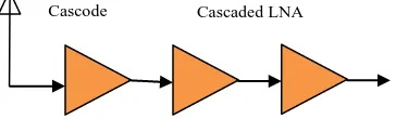
The modern wireless communication systems demand high data rate and high mobility performance during the last few years [1]. WiMAX, which is short for Worldwide Interoperability for Microwave Access, is a novel wireless communication technology. It is an attractive technology due to the high transmitting speed (up to 70Mbps) and long transmitting distance (up to 30 mile). The system bases on IEEE 802.16 standards and uses several bands (2.3-2.7 GHz, 3.4-3.6 GHz and 5.1-5.8GHz) to transmit data. The design of the front-end low noise amplifier (LNA) is one of the challenges in radio frequency (RF) receivers, which needs to provide good input impedance match, enough power gain and low noise figure (NF) within the required band [2].Many high gain amplifier topologies have been proposed as a way to satisfy the requirement for low power dissipation as well as good performances. The cascode with cascaded techniques to produces results in a higher bandwidth and gain, due to the increase in the output impedance, as well as better isolation between the input and output ports [3-7]. Most of the single stage LNA device in the review could only around 20 dB gain. It was proposed that the low noise amplifier should have a gain of at least 30 dB. By taking consideration the extension of communication distance of up to 50 km. A budgeted high gain LNA will ensure a good signal to noise separation for further amplification. For this gain of 50 dB, a cascode with cascaded amplifier is introduced for the LNA as shows in figure 1.
2. THEORETICAL ASPECTS
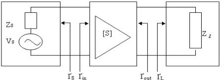
Basically, for designing an amplifier, the input and output matching network are designed to achieve the required stability, small signal gain, and bandwidth. Super high frequency amplifier is a typical active circuit used to amplify the amplitude of RF signal. Basic concept and consideration in design of super high frequency amplifier is presented below. For the LNA designed, the formula and equation were referred to [4]. Figure 2, shows a typical single-stage amplifier including input/output matching networks.
Figure 2: Typical amplifier design
The basic concept of high frequency amplifier design is to match input/output of a transistor at high frequencies using S-parameters frequency characteristics at a specific DC-bias point with source impedance and load impedance. Input/output matching circuit is essential to reduce unwanted reflection of signal and to improve efficiency of transmission from source to load [4-5].
2.1. Power Gain
Several power gains were defined in order to understand operation of super high frequency amplifier, as shown in Figure 3, power gains of 2-port circuit network with power impedance or load impedance at power amplifier represented with scattering coefficient are classified into Operating Power Gain, Transducer Power Gain and Available Power Gain [4-5].
Figure 3: I/O circuit of 2-port network
2.2. Operating Power Gain
Operating power gain is the ratio of power (PL) delivered to the load (ZL) to power (Pin) supplied to 2-port network. Power delivered to the load is the difference between the power reflected at the output port and the input power, and power supplied to 2-port network is the difference between the input power at the input port and the reflected power. Therefore, Operating Power Gain is represented by
2
Where, in indicates reflection coefficient of load at the input port of 2-port network and s is reflection coefficient of power supplied to the input port.
2.3 Transducer Power Gain
Transducer Power Gain is the ratio ofPa vs, maximum power available from source toPL, power delivered to the load. As maximum power is obtained when input impedance of circuit network is equal to conjugate complex number of power impedance, if in=s, transducer power gain is represented by
(2)
Where, L indicates load reflection coefficient.
2.4. Available Power Gain
Available Power Gain, GAis the ratio ofPa vs, power available from the source, toPa vn,
Therefore Available Power Gain is given by:
(3)
That is, the above formula indicates power gain when input and output are matched [5].
2.5. Noise Figure
Signals and noises applied to the input port of amplifier were amplified by the gain of the amplifier and noise of amplifier itself is added to the output. Therefore, SNR (Signal to Noise Ratio) of the output port is smaller than that of the input port. The ratio of SNR of input port to that of output port is referred to as noise figure and is larger than 1 dB. Typically, noise figure of 2-port transistor has a minimum value at the specified admittance given by formula:
(4)
For low noise transistors, manufactures usually provide Fmin,RN,Yopt by frequencies. N defined by formula for desired noise figure:
L
2.6. Condition for Matching
The scattering coefficients of transistor were determined. The only flexibility permitted to the designer is the input/output matching circuit. The input circuit should match to the source and the output circuit should match to the load in order to deliver maximum power to the load. After stability of active device is determined, input/output matching circuits should be designed so that reflection coefficient of each port can be correlated with conjugate complex number as given below [6]:
(6)
(7)
The noise figure of the first stage of the receiver overrules noise figure of the whole system. To get minimum noise figure using transistor, power reflection coefficient should match with
opt
and load reflection coefficient should match with out*
s calculation and simulation using ADS. The S-parameter for each LNA shows in Table I and Table II.
Table I : S-Parameters of Cascode LNA Table II : S-Parameters of Single LNA
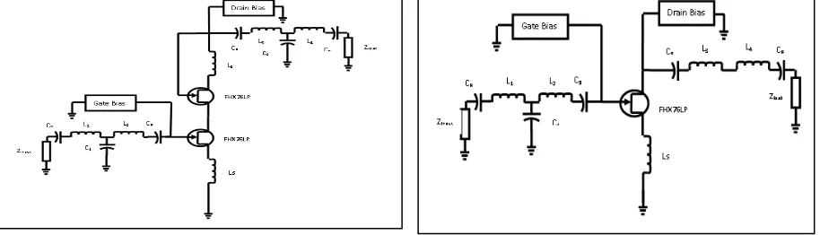
The overall performance of the low noise amplifier is determined by calculating the transducer gain GT, noise figure F and the input and output standing wave ratios, VSWRIN and VSWROUT. The optimum, Γopt and ΓL were obtained as Γopt = 17.354 + j50.13 and ΓL = 79.913-j7.304 for single LNA. While, Γopt = 17.949 + j48.881 and ΓL = 79.913- j7.304 for cascode LNA. Figure 4 shows, the complete schematic circuit of 5.8 GHz a cascode Low noise amplifier. It is called inductive source degeneration. The passive elements in the input matching network are L1, L2 and C1.While; the passive elements in the output matching network are L3, L4 and C2. The load transistor consist of an inductor LD, it is called peaking structure to enhance gain and bandwidth [9]. This transistor also improves the reverse isolation and lowers miller effect [10-13]. Figure 5 shows the completed schematic circuit of 5.8 GHz a single LNA. It also used source degeneration topology and an inductor Ls was inserted to provide the desired input resistance and to improve the stability of amplifier. The
passive elements in the input matching network are L1, L2 and C1. While, inductors L3 and L4 are passive element in the output network. For high gain amplification several amplifier are cascaded in series [11]. It can be designed as one unit or all amplifiers are matched to 50Ω and connected in series. A T-matching network is used to match the input impedance. Using Smith Chart matching techniques, the component values are shown in Table III. To achieve the targeted overall gain of 50dB; it is decided to design cascode and cascaded technique.
Figure 4: The Schematic Circuit for Cascode LNA Figure 5: The Schematic Circuit for Single LNA
Table III: LNA parameters
Items Components of Matching
Cascode LNA Single LNA
L1 6.14 nH 3.661 nH
L2 2.4 nH 0.8799 nH
L3 1.55 nH 3.60 nH
L4 1.62 nH 0.88 nH
C1 0.315 pF 0.5 pF
C2 429.9fF
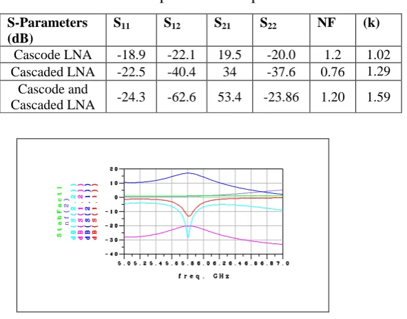
4. SIMULATION RESULT
Table IV: Comparison of output LNA
S-Parameters (dB)
S11 S12 S21 S22 NF (k)
Cascode LNA -18.9 -22.1 19.5 -20.0 1.2 1.02
Cascaded LNA -22.5 -40.4 34 -37.6 0.76 1.29
Cascode and
Cascaded LNA -24.3 -62.6 53.4 -23.86 1.20 1.59
Figure 6a: S-parameters for cascode LNA
Figure 6b: S-parametersfor single cascaded Figure 6c: S-parametersfor cascode and cascaded
5. MEASUREMENT
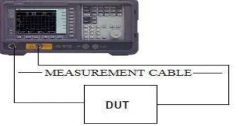
Figure 7: Setup for device under test S Measurement using Network Analyzer
Figure 8: Frequency response measurement setup for device under test.
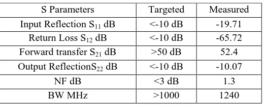
Table V: S-parameters measured
6. RESULT
The result for LNA RF front-end module is presented in Table V. From the tabulated values, the S11 parameter measured is -19.71 dB. This is -9.71 dB less than targeted value which is better and acceptable. S22 measured is -10.07 dB which is less than targeted and acceptable. The return loss required S12 obtained is less than -65.72 dB. The related measured gain S21 for the LNA amplifier is 52.4 dB measured using the setup in Figure 6. The noise figure values obtained from setup in Figure 8 is 1.37 dB which complied with the targeted value of less 3 dB. The use of T lump reactive element and microstrip line matching technique at the input of the LNA contributes the best performance for the amplifier [9]. This matching technique was used to provide high-loaded Q factor for better sensitivity and thus minimized the noise figure. The elements of T-network were realized in the form of lump reactive elements and microstrip line impedance. The 3 dB bandwidth for the amplifier is measured using setup Figure 7. The 3dB bandwidth obtained is 1.24 GHz compliant with targeted result of more than 1 GHz. The measured parameters for the LNA were also compliant with the equation (1) to (9) using MathCAD analysis.
7. CONCLUSION
A low noise amplifier has been simulated and developed successfully with IEEE standard 802.16 WiMAX. It is observed that the simulated and experiment results have not much different. It observed that the gain of the simulated analysis is 53.4 dB and the experimental value is 52.4 dB. It is important to take note when designing the amplifier to match the amplifier circuits. The 5.8GHz LNA has been developed successfully and the circuit cab contributed to the front end receiver at the described frequency. For better performance in gain of the amplifier, it can be achieved by increasing the number of stages to improve the gain and noise figure of the design [11]. Higher gain would expand the coverage or communication distance
S Parameters Targeted Measured
Input Reflection S11 dB <-10 dB -19.71
Return Loss S12 dB <-10 dB -65.72
Forward transfer S21 dB >50 dB 52.4
Output ReflectionS22 dB <-10 dB -10.07
NF dB <3 dB 1.3
REFERENCES
[1] Chia Wei chang and Zhi-Ming Lin (2009), A 1V 14.6 dB Gain LNA for WIMAX 2 - 6GHz Application. IEEE Proceeding.
[2] Ruey-Lue Wang, Shih-Chih Chen, Cheng-Lin Huang, Chien-Hsuan Lie,Yi-Shu Lin (2008), 2-6GHz Current-Reused LNA With Transformer-type Inductors. IEEE Proceeding.
[3] Leon, Michael Angelo G.Lorenzo and Maria Theresa G.De (2010). Comparison of LNA Topology for Wimax Application in a Standard 90-nm CMOS Process. 12th International Conference on Computer Modelling and Simulation. pp-642-647.
[4] M.Pozar, David. Microwave and RF Wireless System (2001), Third Avenue, N.Y.John Wiley & Sons.
[5] Gonzalez, Guillermo (1996), Microwave Transistor Amplifier.
[6] Othman A.R, Hamidon A.H,Ting J.T.H and Mustaffa M.F (2010), High Gain Cascaded Low Noise Amplifier Using T-Matching Network. 4th ISBC 2010.
[7] Weber, Wuezhan Wang and Robert (2003). Design of a CMOS Low Noise Amplifier (LNA) at 5.8GHz and its Sensitivity Analysis. 11th NASA Symposium 2003.
[8] IEEE Computer Society and IEEE Microwave Theory Technique and Society (2004). Part 16 Air Interface For Fix Broadband Wireless System, IEEE Standard 802.16.
[9] Dorra Ayadi, Saul Rodriguez, Mourad Loulou, and Mohammad Ismail (2009). System Level Design of Radio Frequency Receiver for IEEE 802.16 Standard. IEEE Proceeding.
[10] Richard Chi-His Li (2009), RF Circuit Design.
[11] Inder J.Bahl (2009), Fundamentals of RF and Microwave Transistor Amplifier.
[12] Bhartia, P. & Bahl, I (2003), Microwave Solid State Circuit Design, 2nd Edition, J Wiley.