Othman A.R, Ibrahim A.B, Husain M.N,Johal M.S, A.Rashid K.A,Saad M.M Faculty of Electronic and Computer Engineering
Universiti Teknikal Malaysia Melaka. Melaka, Malaysia
Abstract – This paper presents the design and fabrication of radio frequency amplifier (RFA), which operates at 5.8 GHz unlicensed frequency for WiMAX application. The RFA designed used T-matching network consisting of lump reactive elements, 3 dB attenuator and microstrip line at the input and output impedance. The RFA developed in this project contribute a gain of 15.6 dB with overall noise figure of 2.4 dB. The overall measured bandwidth is 1.240 GHz with S parameters S11, S12 and S22 measured are 12.4 dB, -25.5 dB and -12.3 dB respectively. The isolation result shows that there is a significant contribution using 3 dB π -network. The RFA used FET transistor EPA018A from Excelics Semiconductor Inc.
Keywords: Amplifier, Radio Frequency Amplifier, Microstrip
I. I.INTRODUCTION
Recently, the market of wireless communication system is growing rapidly. Due to market demands, there exist various wireless communication systems blooming for different frequency band and different application [1]. The selection of RF circuit components including low noise amplifier (LNA), Radio Frequency (RF) amplifier and filters for the transmitter and receiver can make or break an entire wireless system [2]. The RF receiver system would have to be well designed, so that a high performance of communication link can be achieved.
The progress of wireless communication services has increased the need for designing RF communication systems which have multi-band capability with high gain, better input sensitivity and a minimum noise level. It was desirable to combine two or more standards in one mobile unit for overall capacity enlargement, higher flexibility and roaming capability as well as backward compatibility. Moreover multi standard RF receivers would allow access to different systems provided by various providers.
The device chosen for the RF amplifier will be selected based on the input sensitivity which was now at -80 dBm. Once the device is chosen the device parameter will have to be matched for maximum power transfer. At the same time added isolation can be provided by incorporating a matched 50 ohm Π network into the system. This also acts as a buffer
for the next stage design. The FET transistor EPA018A from Excelics Semiconductor Inc was selected since it operates at required input sensitivity and bandwidth.
With WiMAX, RF transceiver system are breaking the bonds of wired connections in between separated buildings especially in area where wired bridge is impossible to be deployed. WiMAX wireless technology is more economical and efficient than installing wired networks. With the current technology of Orthogonal Frequency Division Multiplexing (OFDM) adopted in IEEE 802.16 WiMAX, the system can provide a high data rate of up to 70 Mbps [3]. The RF Amplifier in WiMAX plays an important role before converting baseband signal from the transmitted RF signal so that the system can communicate wirelessly. Therefore, the performance of the WiMAX system relies on the RF front-end receiver system that should be well designed to minimize the noise level (or distortions) in the system [7]. The approach taken in designing the amplifiers involves a series of chronological steps. No design is complete without some desired goals. The design specifications for the radio frequency amplifier were shown in Table I:
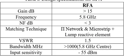
Table I: Design specifications for RFA RFA
Gain dB > 15
Frequency 5.8 GHz
NF dB < 3
Matching Technique Π Network & Microstrip + Lump reactive element
VSWR 1.5
Bandwidth MHz >1000(5.8 GHz Centre)
Input sensitivity - 55 dBm
With refer to Table I the gain targeted for the RF Amplifier was more than 15 dB. This gain was necessary to amplify week signals and separated from the noise. The amplifier will maintain noise figure less than 3 dB and provide bandwidth above 1000 MHz. The input sensitivity for the RFA was set at -80 dBm compliant with the standard WiMAX application.
Design and Fabrication of Radio Frequency
Amplifier with 3 dB
π
-Network Attenuator
2 design, formula and equation were referred to [2]. Figure 1 shows a typical single-stage amplifier including input/output matching networks.
Figure 1: Typical amplifier designed
The basic concept of high frequency amplifier design is to match input/output of a transistor at high frequencies using S parameters [S] frequency characteristics at a specific DC-bias point with source impedance and load impedance. Input/output matching circuit is essential to reduce the unwanted reflection of signal and to improve efficiency of the transmission from source to load. The targeted specification amplifier is shown in Table I.
A. Power Gain
Several power gains were defined in order to understand the operation of super high frequency amplifier, as shown in Figure 2, power gains of 2-port circuit network with power impedance or load impedance at power amplifier represented with scattering coefficient are classified into Operating Power Gain, Transducer Power Gain and Available Power Gain[2],[6].
Figure 2: I/O circuit of 2-port network
B. Operating Power Gain
Operating power gain is the ratio of power (P L ) delivered to the load (ZL) to power (Pin) supplied to 2 port network. Power delivered to the load is the difference between the power reflected at the output port and the input power port, and power supplied to the 2-port network are the difference between the input power at the input port and the reflected power. Therefore, Operating Power Gain is input port of 2-port network and s is reflection coefficient of power supplied to the input port.
C. Transducer Power Gain
Transducer Power Gain is the ratio of
P
avs, maximum power available from source toP
L, power delivered to the load. As maximum power is obtained when input impedance of circuit network is equal to conjugate complex number of power impedance, if in= s, transducer power gain is represented by
(2)
Where, L indicates load reflection coefficient.
D. Available Power Gain
Available Power Gain,
G
Ais the ratio ofP
avs, power available from the source, toP
avn, power available from 2-port network, represents,That is, the above formula indicates power gain when input and output are matched.
E. Noise Figure output port is referred to as noise figure and is larger than 1 dB. Typically, noise figure of 2-port transistor has a minimum value at the specified admittance given by formula:
(4)
For low noise transistors, manufactures usually provide opt F. Condition for Matching
The scattering coefficients of transistor were determined. The only flexibility permitted to the designer is the input/output matching circuit. The input circuit should match to the source and the output circuit should match to the load in order to deliver maximum power to the load. After stability of active device is demanded, input/output matching circuits should be designed so that reflection coefficient of each port is correlated with conjugate complex number as given below:
L overrules noise figure of the whole system. To get minimum noise figure using transistor, power reflection coefficient should match with opt and load reflection coefficient should match with out*
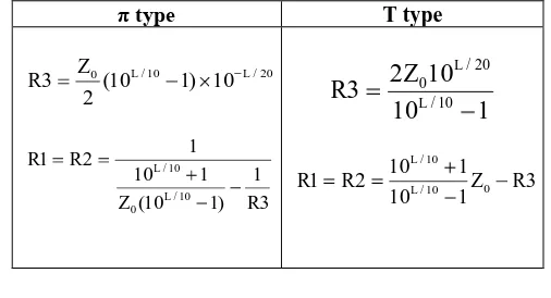
s= opt (8) to the input, the gain will be reduced to the specification and the input match will improved. The attenuator is not suitable for the amplifier design that concern about the noise figure since the dB attenuation will increase the corresponding noise figure. Figure 3 shows two types of fixed attenuator, which is T type, and π type and the related equations shown in Table II.
Figure 3 π type and T type attenuator
The resistance value can be calculated when the attenuation volume selected.
Table II. π type and T type attenuator formula
0.989. This showed a clear tendency for oscillation which confirmed the calculated stability factor. The calculated transducer power gain for matched condition was 16.28 dB. The input matching for optimum
Γ
opt andL
Γ
were obtained asΓ
opt = 12.662 +j 38.168 andL
Γ
= 79.97- j7.286. The noise figure calculated is 2.475 dB.
For the input matchingΓ
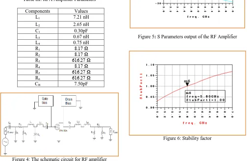
opt, it is required to provide high loaded Q factor for better sensitivity. A T-network was used to match the impedance.For the output impedance ΓL, since the impedance is real, suitable matching impedance for the load is by using quarter-wave transformer. The RF amplifier can also act as an isolator for the overall front-end system and a suitable Π -network with 50 Ώ load impedance was inserted at the input and output of the amplifier to provide a 3 dB insertion loss each for the network. Using Smith Chart matching technique, the component values are shown in Table III. The DC block capacitor was selected for the circuit and the value is recommended at least 10 times from the C1. For this reason 7.5 pF capacitors are selected as bypass capacitors. With these components, the schematic circuit for RF Amplifier is shown in Figure 4.
Table III: RFA Amplifier Parameters
Components Values
L1 7.21 nH
L2 2.65 nH
C1 0.30pF
L3 0.67 nH
L4 0.75 nH
R1 8.17 Ω
R2 8.17 Ω
R3 616.27 Ω
R4 8.17 Ω
R5 616.27 Ω
R6 616.27 Ω
CB 7.50pF
Figure 4: The schematic circuit for RF amplifier
IV. SIMULATION
The related S parameters output of the amplifier is shown in Figure 5. The simulated S parameter results in Figure 5 show that the S21 gain at 5.8 GHz is 15.28 dB. The corresponding input return loss S11, output return loss S22 and reflection loss S12 were -16.58 dB,-12.52dB and -20.06 dB. The noise figure output observed is -2.19 dB. For this amplifier, the consideration is on the maximum gain with noise figure less than 3 dB. This S parameter output is acceptable with the targeted specification required for the system. The stability factor after matching load is shown in Figure 5 and Figure 6. Figure 5 shows the stability factor while Figure 7 shows the obtained noise figure (NF) is 2.19 and VSWR observed is 1.41. These parameters were compliant with the targeted specifications of the amplifier for unconditional stable condition k is 1 and VSWR is targeted as 1.5. The noise figure output observed is 2.19.
Figure 5: S Parameters output of the RF Amplifier
Figure 7: Noise Figure
Table IV shows the targeted and the simulated s parameter for the amplifier.
Table IV: S Parameter Output and Targeted Parameters of RFA
The designed circuit is sent for fabrication and the LNA layout is shown in Figure 8 and Figure 9 shows the fabricated of RF amplifier.
Figure 8: Layout of RF amplifier
Figure 9: Fabricated of RF Amplifier
V. MEASUREMENT
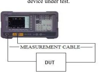
Referring to the measurement setup shown in Figure 10, the S parameter measurement is carried out for the RF amplifier. The S11, S12, S21 and S22 were also measured using the network analyzer. The gain of the amplifier was measured using the setup Figure 11. The noise figure values and 3 dB bandwidths were obtained from setup Figure 12. Before all measurement was recorded, a standard procedure of calibration was followed to ensure that the measurement tools were calibrated.
Figure 10: Setup for device under test S Measurement using Network Analyzer
Figure 11: Frequency response measurement setup for device under test.
Figure 12: Measurement setup for device under test for Noise Figure
VI. RESULT
The result for RF amplifier is presented in Table V.
S Parameters Targeted
RFA
Simulated RFA Input reflection S11 dB -10 -16.58
Return Loss S12 dB -10 -20.06 Forward Transfer S21 dB 15 15.28 Output Reflection loss S22 dB -10 -12.52 Noise Figure NF dB * <3 2.19
Table V: S Parameter result for LNA
S Parameters Targeted Measured
Input Reflection S11 dB <-10 dB -12.4
Return Loss S12 dB <-10 dB -25.5
Forward transfer S21 dB >15 dB 15.6
Output ReflectionS22 dB <-10 dB -12.3
NF dB * <3 dB 2.4
BW MHz >1000 1125
From the tabulated values, the S11 parameter measured is -12.4 dB. This is -4.18 dB less than targeted which is better and acceptable. S22 measured is -12.3 dB which is less than targeted and acceptable. The return loss required S12 obtained is less than -25 dB which is also acceptable and better. The use of Π-network with 50 Ώ load impedance at the input and output of the RF Amplifier shows a better return loss which is lower than -25 dB. The minimum return loss targeted for this amplifier is less than -10 dB. The related measured gain S21 for the RF amplifier is 15.6 dB measured using the setup Figure 10 and 11. The noise figure values obtained from setup Figure 12 is 2.4 dB which complied with the targeted value of 3dB. . Again shows that the use of T lump reactive element and microstrip matching network provide best performance for the RF Amplifier since the measure value nearly optimized. The 3dB bandwidth for the amplifier is measured using setup Figure 10. The 3dB bandwidth obtained is 1125 MHz which is more than the targeted result of 1000 MHz.
VII. CONCLUSION
A 5.8 GHz radio frequency amplifier with 3 dB network attenuator isolation was designed and developed. The configuration of 3 dB π-networks has significant with the measured of isolation. This RF front-end receiver is capable of providing a better pipeline for the receiver with minimum noise figure and provides a high gain. The overall result shown, there is an improved of reverse isolation (S12). This output is acceptable for further processing of the baseband system for IEEE 802.16 WiMAX standard.
REFERENCES
[1] Ruey-lue Wang,Shih-Chih Chen, Cheng-Lin Huang, Yi-Shu Lin. “ 2-6 GHz Current-Reused LNA with Transformer-Type Inductor”. IEEE Proceeding, 2008. [2] David M. Pozar. 2001, „Microwave and RF Wireless
System’. Third Avenue, N.Y.: John Wiley &Sons,In
[3] Xuezhen Wang and Robert Weber,”Design a CMOS Low Noise Amplifier (LNA) at 5.8 GHz and its sensitivity analysis”, 11th NASA Symbosium, 2003. [4] Institute of Electrical and Electronic Engineering (IEEE).
1999,‟IEEE Standard: Part 11, Wireless LAN Medium Access Control (MAC) and Physical Layer (PHY) specifications: High-speed Physical
Layer in the 5 GHz Band. IEEE 802.11a.‟
[5] Jui-Hung Yeh, Jyh-Cheng Chen, Chi-Chen Lee. Oct./Nov. 2003, WLAN standards’:. Potentials IEEE. . 22(4): pg16 – 22
[6] Man & Tel Co.Ltd, 2006, MW-2000 Microwave Communication Trainer , Manual Trainer
[7] Bahl, I. & Bhartia, P. (2003). Microwave Solid State Circuit Design, 2nd Edition, J Wiley, pp. 133-180.
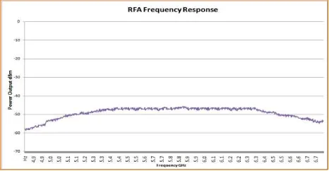
The Figure 13 shows the frequency response after injecting -60 dBm signals. The output power is -44.4 dBm. The measured parameters for the RF were also compliant with the formulae (1) to (9) using MathCAD analysis.
Figure 13: Frequency Response RF amplifier