TELKOMNIKA, Vol.14, No.4, December 2016, pp. 1213~1216 ISSN: 1693-6930, accredited A by DIKTI, Decree No: 58/DIKTI/Kep/2013
DOI: 10.12928/TELKOMNIKA.v14i4.4788 1213
Received September 11, 2016; Revised October 26, 2016; Accepted November 10, 2016
Editorial
Numerical Investigation of a New Junctionless
Phototransistor for High-performance and Ulta-low
Power Infrared Communication Applications
H. Ferhati1, F. Djeffal*2, T. Bentercia3
1,3LEA, Department of Electronics, University of Batna 2, Batna 05000, Algeria
2
LEPCM, University of Batna 1, Batna 05000, Algeria
*Corresponding author, email: [email protected], [email protected]
Abstract
In this paper, a new junctionless optical controlled field effect transistor (JL-OCFET) is proposed to improve the device performance as well as achieving low power consumption. An overall optical and electrical performances comparison of the proposed junctionless design and the conventional inversion mode structure (IM-OCFET) has been developed numerically, to assess the optical modulation behavior of the OCFET for low power optical interconnections applications. It is found that, the proposed design demonstrates excellent capability in decreasing the phototransistor power consumption for inter-chip optical communication application. Moreover, the proposed device offers superior sensitivity and ION/IOFF ratio, in addition to lower signal to noise ratio as compared to the conventional IM-OCFET structure. The obtained results indicate the crucial role of the junctionless (JL) design in enhancing the phototransistor performance and reducing the total power dissipation. Such a very sensitive OCFET can be very promising in the future low power optical receiver less compatible to CMOS modern technology for high-quality inter-chips data communication applications.
Keywords: Junctionless, OCFET, Sensitivity, CMOS, Power consumption.
Copyright © 2016 Universitas Ahmad Dahlan. All rights reserved.
In the long-haul telecommunication system, the huge power consumption by the traditional transmission wires is an important limitation which degrades the communication system performance in terms of cost and power dissipation [1-2]. However, optical interconnects are considered as a good solution to remedy the problems faced by electric wires and can refashion the inter-chip data communications systems [2-4]. The quality of optical receivers in optical wireless communication systems (OWCS) greatly determines the total power consumption in these systems, where it is crucial to develop receivers’ with faster and efficient response. In this context, several published works deal with numerous optical receivers’ structures based on Schottky barrier photodiode, MSM photodetectors and FET-based phototransistor [5-8]. This latter is considered as the most common device due to the opportunity for avoiding the high density of the optical circuits namely Trans-Impedance Amplifier (TIA) and the limiting amplifiers used in readout circuit. These amplifiers constitute a serious impediment in high-performance communication compatible with CMOS technology. Previously, different scientific endeavors have originated the OCFET with IV group material or germanium (Ge) sensitive gate [7-10]. The operating mechanism of this device dwells on exploiting the photo-generated carriers to modulate the band bending in the transistor, and thus changes the output current. However, the Ge-based OCFET operating at an appropriate wavelength of ( =1.55 m), seems to be preferable for infrared communication due to the low optical band gap and the high carrier mobility offered by the Ge semiconductor. Besides, the excellent compatibility of the Ge material to be growing on Si platform leads to an ultra-high sensing performance, large bandwidth and efficient compatibility with state-of-art CMOS
ISSN: 1693-6930
TELKOMNIKA Vol. 14, No. 4, December 2016 : 1213 – 1216 1214
These persistent problems adversely affect the device optical and electrical performance for chip-level infrared optical communication. Hence, it is of great significance to propose lower cost designs, enhance the electrical behavior of the conventional Ge-based OCFET and make it consumes less power. For achieving this objective, the JL design can be considered as a paramount solution for reaching the desired improvement in fabrication process cost. In this framework, the main advantage offered by this design resides principally on avoiding the formation of the source/drain regions (n++) and hence the establishment of junctions which seems to be an intractable task. Several experimental studies have confirmed the low-cost fabrication of the JL structure in comparison with the conventional IM design, where uniform n -type channel doping is sufficient to conduct the transistor [13-16]. In this paper, we propose a new JL-OCFET to enhance the device performance and achieve low power consumption. We perform also an overall optical and electrical performances comparison of the proposed JL
design and the conventional one.
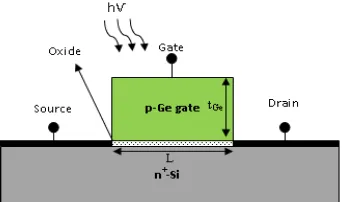
The proposed junctionless design is built principally on the suppression of the source/drain regions and adopting uniform n-type channel doping. In order to obtain an initial band bending, we assume the Ge gate in our proposed JL-OCFET with p-type doping. To this extent, Figure 1 shows the cross-sectional view of the proposed junctionless design, where NGe and NSi are the Ge gate and the Si channel doping concentration, respectively, L represents the channel length and tGerefers to the germanium thickness.
Figure 1. Cross sectional view of the proposed JL-OCFET phototransistor.
For our numerical investigation, we use Atlas 2-D simulator [16], to develop the numerical model of the proposed design that is more accurate and allows evaluating the JL-OCFET electrical behavior for the optical communication application. The photo-generated current in the Ge gate is calculated using the solution of Poisson’s equation and continuity equations. To describe the carrier recombination mechanism, Fermi model and recombination models (Shockley–Read–Hall (SRH), Auger and surface recombination) are also included. Furthermore, due to the high level doping in the junctionless design, the carrier mobility is taken dependent on the doping concentration.
The principal aspect of the OCFET is the optical modulation behavior of the output current using different incident power with an appropriate wavelength value. Hence, in order to evaluate the proposed design regarding this aspect, we illustrate in Figure 2(a) the transfer characteristics of the proposed JL-OCFET with different incident power for a fixed gate voltage value of (Vgs=-1V).
It is clearly observed from this figure, the simple and the good operating behavior of the
TELKOMNIKA ISSN: 1693-6930
Numerical Investigation of a New Junctionless Phototransistor for… (H. Ferhati)
1215
1E-10 1E-9 1E-8 1E-7 1E-6 1E-5 1E-4 0 Figure 2.(a) I–V characteristics of the proposed JL OC-FET for different optical powers, with
NSi = 1×1018cm−3, NGe = 1×1018 cm−3, Vgs = -1V and L=180nm. (b) Drain current as a function of the optical power with Vgs = -1V and Vds = 0.5V
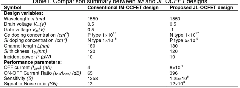
In order to elucidate the performance improvement of the proposed JL design over the conventional IM-OCFET, it is important to compare the electrical performance provided by both devices. For this purpose, Table 1 summarizes the overall electrical and optical performance comparison between both IM and JL OCFET designs. From this table, it is demonstrated that the device figures of merit (FoMs) regarding the power consumption are greatly improved compared to the conventional counterpart. Moreover, the proposed JL design exhibits superior sensitivity, which makes it valuable for low cost and low power consumption receiver for high-performance chip-level infrared communication applications.
Table1. Comparison summary between IM and JL OCFET designs
Symbol Conventional IM-OCFET design Proposed JL-OCFET design
Design variables:
[1] A Krishnamoorthy, H Schwetman, X Zheng, R Ho. Energy-Efficient Photonics in Future
High-Connectivity Computing Systems. Journal Of Lightwave Technology. 2015; 33(4): 889-900.
[2] N Kannan, MJ Kumar. Technology and reliability constrained future copper interconnects. IEEE Trans.
Electron Devices. 2002; 49: 590-597.
[3] S Manipatruni, M Lipson, IA Young. Device Scaling Considerations for Nanophotonic CMOS Global
Interconnects. IEEE Journal of Selected Topics in Quantum Electronics. 2013; 19: 1077-1086.
[4] DAB Miller. Physical reasons for optical interconnections. Intl. Journal of Optoelectronics. 1997; 11:
155-168.
[5] JS Liu, CX Shan, BH Li, ZZ Zhang, CL Yang, DZ Shen, XW Fan. High responsivity ultraviolet
photodetector realized via a carrier-trapping process. Applied physics latters. 2010; 97(25):
251102-251105.
[6] UM Nayefa, KA Hubeatirb, ZJ Abdulkareemba. Ultraviolet photodetector based on TiO2
nanoparticles/porous silicon hetrojunction. Optik. 2016; 126: 2806-2810.
[7] L Colace, V Sorianello, S Rajamani. Investigation of Static and Dynamic Characteristics of Optically
ISSN: 1693-6930
TELKOMNIKA Vol. 14, No. 4, December 2016 : 1213 – 1216 1216
[8] RW Going, J Loo, TK Liu, MC Wu. Germanium gate photo MOSFET integrated to Silicon photonics.
IEEE J. Sel. Top. Quantum Electron. 2014; 20(4), 8201607.
[9] F Djeffal, H Ferhati. A new high-performance phototransistor design based on both surface
texturization and graded gate doping engineering. Journal of Computational electronics. 2016; 15:
301-310.
[10] H Ferhati, F Djeffal. Role of gradual gate doping engineering in improving phototransistor performance
for ultra-low power applications. Journal of Computational electronics. 2016; 15: 550-556.
[11] L Colace, G Assanto. Germanium on Silicon for near-infrared light sensing. IEEE Photonics J. 2009;
1(2): 69-79.
[12] J Michel, J Liu, LC Kimerling. High-performance Ge-on-Si photodetectors. Nat. Photonics. 2010; 4(8):
527-534.
[13] CW Lee, A Afzalian, ND Akhavan, R Yan, I Ferain, JP Colinge. Junctionless multigate field-effect transistor. Appl. Phys. Lett. 2009; 94: 053-511. 2009.
[14] JP Colinge. Multi-gate SOI MOSFETs. Solid-State Electron. 2004; 48(6): 897-905.
[15] JP Colinge, CW Lee, A Afzalian, ND Akhavan, et al. Nanowire transistors without junctions. Nat.
Nanotechnol. 2010; 5(3): 225-229.