ANALOG VERY LARGE SCALED OF INTEGRATION (VLSI) TESTING AND ANALYSIS OF COMBINATIONAL CIRCUITS USING
COMPUTER-AIDED DESIGN (CAD) TOOLS
CHONG MIN WEN
This report is submitted in partial fulfillment of the requirements for the award of Bachelor of Electronic Engineering (Computer Engineering)
with Honours
Faculty of Electronic and Computer Engineering Universiti Teknikal Malaysia Melaka
UNIVERSITI TEKNIKAL MALAYSIA MELAKA
FAKULTI KEJURUTERAAN ELEKTRONIK DAN KEJURUTERAAN KOMPUTER
BORANG PENGESAHAN STATUS LAPORAN PROJEK SARJANA MUDA II
Tajuk Projek : Analog Very Large Scaled of Integration (VLSI) Testing and Analysis of Combinational Circuits Using Computer-Aided Design (CAD) Tools
Sesi
Pengajian : 2008/2009
Saya CHONG MIN WEN mengaku membenarkan Laporan Projek Sarjana Muda ini disimpan di Perpustakaan dengan syarat-syarat kegunaan seperti berikut:
1. Laporan adalah hakmilik Universiti Teknikal Malaysia Melaka.
2. Perpustakaan dibenarkan membuat salinan untuk tujuan pengajian sahaja.
3. Perpustakaan dibenarkan membuat salinan laporan ini sebagai bahan pertukaran antara institusi
pengajian tinggi.
4. Sila tandakan ( ) :
SULIT*
(Mengandungi maklumat yang berdarjah keselamatan atau kepentingan Malaysia seperti yang termaktub di dalam AKTA RAHSIA RASMI 1972)
TERHAD* (Mengandungi maklumat terhad yang telah ditentukan oleh
organisasi/badan di mana penyelidikan dijalankan)
TIDAK TERHAD
Disahkan oleh:
__________________________ ___________________________________
(TANDATANGAN PENULIS) (COP DAN TANDATANGAN PENYELIA)
“I hereby declare that this report is the result of my own work except for quotes as cited in the references.”
Signature : ………..
Author : CHONG MIN WEN
“I hereby declare that I have read this report and in my opinion this report is sufficient in terms of the scope and quality for the award of Bachelor of Electronic
Engineering (Computer Engineering) with Honours.”
Signature : ………..
Supervisor’s Name : MADAM WONG YAN CHIEW
ACKNOWLEDGEMENT
First and foremost, I would like to extend my appreciation to my supervisor, Madam Wong Yan Chiew for all her guidance, comments, suggestion and constructive criticism for my project. Under her guidance, I have learned a lot along the way and she has helped me all the way through. She was patient to teach me and guide me to the right way to complete my project. Also, I would like to show my utmost thanks to my family who has given me support throughout my academic years.
ABSTRACT
ABSTRAK
CONTENT
CHAPTER TOPIC PAGE
TITLE i
DECLARATION ii
DEDICATION v
ACKNOWLEDGEMENT vi
ABSTRACT vii
ABSTRAK viii
CONTENT ix
LIST OF TABLE xii
LIST OF FIGURE xiii
LIST OF ABBREVIATION AND SYMBOL xv
LIST OF APPENDIX xvii
I INTRODUCTION 1
1.1 Introduction 1
1.2 Objective 2
1.3 Problem Statement 2
1.4 Scope 2
1.5 Methodology 3
1.6 Thesis Outline 3
1.7 Conclusion 4
2.1 Combinational Circuit 5
2.1.1 Multiple-Input AND Gate 12
2.1.2 Comparator 13
2.1.3 Decoder 14
2.1.4 Multiplexer and Demultiplexer 16
2.1.5 Adder 18
2.1.6 Operational Amplifier (Op-Amp) 20 2.2 Very Large Scaled of Integration (VLSI) Testing 22
2.2.1 VLSI Technology 22
2.2.2 Functional Testing 22
2.2.3 Fault Model Based Testing 23 2.3 Computer-Aided Design (CAD) Tools 25
2.3.1 Multisim 25
2.3.2 MATrix LABoratory (Matlab) 26
2.4 Conclusion 27
III METHODOLOGY 28
3.1 Flow Chart 28
3.2 Fault Model Based Testing 30
3.3 Transistor 30
3.4 Analog Testing 32
3.4.1 Logic Gate 32
3.4.2 Combinational Circuits 35
3.5 Circuit Analysis and Graphical User Interface (GUI) 38
3.6 Conclusion 38
4.1 Schematic Simulation in Multisim 40 4.2 GUI and Analog Testing Analysis 42
4.2.1 NOT Gate Analysis 45
4.2.2 OR Gate Analysis 47
4.2.3 AND Gate Analysis 49
4.2.4 NOR Gate Analysis 51
4.2.5 NAND Gate Analysis 52
4.2.6 Half-Adder Analysis 54
4.2.7 2-to-4 Decoder Analysis 58
4.3 Discussion 61
4.4 Conclusion 62
V CONCLUSION AND DISCUSSION 63
5.1 Conclusion 63
5.2 Recommendation 64
REFERENCE 65
LIST OF TABLE
NO TITLE PAGE
2.1 Truth Tables of Logic Gates 6
2.2 Logic Gates 7
2.3 Truth Table of 1-Bit Comparator 13
2.4 Inputs and Outputs of 2-to-4 Decoder 16
2.5 Inputs and Outputs of 3-to-8 Decoder 16
2.6 Truth Table of Single Bit 4-to-1 Line Mux 17 2.7 Truth Table of Single Bit 1-to-4 Line Demux 17
2.8 Multiplexer and Demultiplexer 18
2.9 Truth-Table of Half-Adder 19
2.10 Truth Table of Full-Adder 20
2.11 Types of Fault in Analogue Circuits 23
4.1 NOT Gate Simulation Results 47
4.2 OR Gate Simulation Results 49
4.3 AND Gate Simulation Results 50
4.4 NOR Gate Simulation Results 52
4.5 NAND Gate Simulation Results 54
4.6 Half-Adder Simulation Results 56
4.7 Analysis on the Half-Adder Output Pattern 57
4.8 2-to-4 Decoder Simulation Results 59
4.9 Output Waveform of Decoder 60
LIST OF FIGURE
NO TITLE PAGE
2.1 Transistor XOR Gate 10
2.2 Transistor XNOR Gate 11
2.3 8-Input AND Gate with Seven 2-Input AND Gate Connected in
Series 12
2.4 8-Input AND Gate with Seven 2-Input AND Gate Connected in
as Much as Parallelism as Possible 13
2.5 1-Bit Comparator 13
2.6 4-Bit Comparator 14
2.7 2-to-4 Decoder 15
2.8 3-to-8 Decoder 15
2.9 Half-Adder 19
2.10 Full-Adder 20
2.11 A Simple Op-Amp Made from Discrete Components 21
3.1 Process of the Project 29
3.2 NPN BJT 31
3.3 PNP BJT 31
3.4 Transistor 31
3.5 NOT Gate 33
3.6 OR Gate 33
3.7 AND Gate 34
3.8 NOR Gate 34
3.10 Half-Adder in Transistor Level 36
3.11 2-to-4 Decoder in Transistor Level 37
4.1 Schematic in Multisim 40
4.2 Schematic Simulation in Multisim 41
4.3 Layout Design of GUI 42
4.4 GUI after Run 43
4.5 “How do transistor work?” Button 44
4.6 GUI after a Circuit Button is Selected 45
4.7 NOT Gate Simulation Circuit 46
4.8 OR Gate Simulation Circuit 47
4.9 AND Gate Simulation Circuit 49
4.10 NOR Gate Simulation Circuit 51
4.11 NAND Gate Simulation Circuit 53
4.12 Half-Adder Simulation Circuit 55
LIST OF ABBREVIATION AND SYMBOL
- Open loop DC gain
B - base
BJT - bipolar junction transistor
C - collector
CAD - Computer-Aided Design CMRR - Common mode rejection ratio
dB - decibels
Demux - demultiplexer
E - emitter
GBW - Gain bandwidth product GUI - Graphical User Interface
GUIDE - graphical user interface development environment - Input bias current
IC - integrated circuit
m - milli
Matlab - MATrix LABoratory
MOSFET - Metal Oxide Semiconductor Field Effect Transistor Mux - Multiplexer
n - nano
Op-amp - operational amplifier
PSRR - Power supply rejection ratio
SR - Slew rate
Vos - Input offset voltage
SPICE - Simulation Program with Integrated Circuit Emphasis
Vin - input voltage
VLSI - Very Large Scaled of Integration Vout - output voltage
LIST OF APPENDIX
NO TITLE PAGE
A Coding of Matlab GUI 66
CHAPTER I
INTRODUCTION
This chapter introduces this project in which the project is Very Large Scaled of Integration (VLSI) based. The circuits use in the project is combinational circuit and software involves are Multisim and MATrix LABoratory (Matlab). Besides that, the objectives, problem statements and scopes of project are described in this chapter. Next, the methodology shows the implementation of the project and the contents of each chapter are introduced in thesis outline.
1.1 Introduction
1.2 Objective
There are five objectives to be achieved in this project: - To characterize combinational circuits.
- To study the effects of circuit’s parameters to its performance. - To perform the analog testing.
- To analysis the result of testing.
- To create a GUI to provide users a media to explore and analyze the analog circuit testing.
1.3 Problem Statement
Nowadays, in VLSI technology in electronics field, it is possible to produce a die with millions of transistors on it so that a total system can be produced on a single chip. The chips are developed with decreasing physical dimensions of the transistors. The reduction in physical dimensions of the transistors will then increases the probability of manufacturing defect in the integrated circuit (IC) and hence results in a faulty chip. The entire chip might not properly function even though only a transistor is defected. For instance, the chip will not function at the required operating frequency due to only one faulty transistor in a chip. Hence, testing is required to guarantee fault free products as the defect chips are disallowed during the manufacturing process.
1.4 Scope
graphical user interface (GUI). Besides that, the GUI is functioned as a user interface to explore and analyze analog circuit testing through it.
1.5 Methodology
The project is started with the literature review on the VLSI testing and the combinational circuit. After that, several combinational circuits are chosen and constructed in Multisim. The circuits are simulated using appropriate VLSI testing. The circuit simulation is started with the simple circuits which are basic logic gates and some others logic gates and following by more complex circuits. The circuits are simulated for fault free and also with their resistors opened and shorted. The simulation results are then collected for used in Matlab GUI.
The next step is to come out a GUI using Matlab. The GUI is created and designed by using the combination of GUI layout design editor as well as source code editor. From the GUI, it shows the waveforms of the testing results after the button of the desired circuit is being selected. From the waveforms, the testing results are analyzed. Also, the testing results of the fault free circuits are compared with their circuits with parametric variation.
1.6 Thesis Outline
This thesis is wrote to provide information about the final year project perform by final year student of Universiti Teknikal Malaysia Melaka (UTeM). There are five chapters contains in this thesis.
Chapter 2 covers the literature review of the project. Combinational circuits and several examples of this category of circuit are mentioned here. Also, analog VLSI testing and its types are discussed in this chapter. Another topic to be covered here is the CAD tools used in the project.
Chapter 3 provides the methodology of the project and the reason for choosing these methods. Also, the project flow is shown in this chapter.
Chapter 4 delivers the results of the project which included the simulation results and the analysis on it. Besides that, the discussion included problems faced, results from circuit simulation and analysis are presented in this chapter.
The last chapter is the conclusion of the project. Other than that, there are some suggestions for future development of the project.
1.7 Conclusion
CHAPTER II
LITERATURE REVIEW
This chapter explains the literature review of the project which including the introduction of several combinational circuits, several test methods of the VLSI testing and the CAD tools use to implement the project. A number of circuits discussed in this chapter are chosen for simulation and analysis. In addition, the test methods are compared in order to choose the one that is more applicable for the circuits.
2.1 Combinational Circuit
Generally, there are two basic categories of circuits in electronics field which are combinational circuit and sequential circuit. Different from sequential circuit where the outputs is depend on the current and past inputs, combinational circuit using only the current inputs to produce outputs [3]. The inputs are combined in someway to produce the outputs [3].
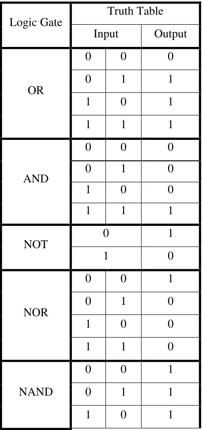
From Table 2.1, it shows that the OR gate will gives high output when at least one of the inputs is high. However, it is different for AND gate. AND gate produces high output only when all of the inputs are high. NOT gate is also known as inverter. Same as its name, NOT gate always gives the output which is the inversion of its input. For NOR gate, it inverts the output of OR gate. It produces high output only when all of the inputs are low. NAND gate shows low output when all of the inputs are high. When both of the inputs are same, XOR gate will shows low output. On the other hand, XNOR gate will gives high output as both of the inputs are same.
[image:23.595.217.422.313.748.2]
Table 2.1 Truth Tables of Logic Gates
Logic Gate
Truth Table Input Output
OR
0 0 0
0 1 1
1 0 1
1 1 1
AND
0 0 0
0 1 0
1 0 0
1 1 1
NOT
0 1
1 0
NOR
0 0 1
0 1 0
1 0 0
1 1 0
NAND
0 0 1
0 1 1
1 1 0
XOR
0 0 0
0 1 1
1 0 1
1 1 0
XNOR
0 0 1
0 1 0
1 0 0
1 1 1
[image:24.595.215.422.83.294.2]The logic gates in gate level and their corresponding transistor level are implemented in Table 2.2. NOT gate and single transistor NOR gate use only a transistor whereas double transistor NOR gate, OR, AND and NAND gates use two transistor in their circuit.
Table 2.2 Logic Gates
Logic Gate Gate Level Transistor Level