HAMMING CODE USING FIELD PROGRAMMABLE GATE ARRAY (FPGA)
SITI BASIRAH BINTI AMIR HAMZAH
This Report Is Submitted In Partial Fulfilment of Requirements For The Bachelor Degree of Electronic Engineering (Computer Engineering)
Faculty of Electronic Engineering (Computer Engineering) Universiti Teknikal Malaysia Melaka
UNIVERSTI TEKNIKAL MALAYSIA MELAKA FAKULTI KEJURUTERAAN ELEKTRONIK DAN KEJURUTERAAN
KOMPUTER
BORANG PENGESAHAN STATUS LAPORAN PROJEK SARJANA MUDA II
TajukProjek : ……….
SesiPengajian : 1 3 / 1 4
Saya ………..
mengakumembenarkanLaporanProjekSarjanaMudainidisimpan di Perpustakaandengansyarat-syaratkegunaansepertiberikut:
1. LaporanadalahhakmilikUniversitiTeknikal Malaysia Melaka.
2. Perpustakaandibenarkanmembuatsalinanuntuktujuanpengajiansahaja.
3. Perpustakaandibenarkanmembuatsalinanlaporaninisebagaibahanpertukaranantarainstitusipen gajiantinggi.
4. Silatandakan ( √ ) :
SULIT* *(Mengandungimaklumat yangberdarjahkeselamatanataukepentingan Malaysia seperti yang
termaktubdi dalam AKTA RAHSIA RASMI 1972)
TERHAD** **(Mengandungimaklumatterhad yang telahditentukanolehorganisasi/badan di manapenyelidikandijalankan) TIDAK TERHAD Disahkanoleh: ___________________________ (TANDATANGAN PENULIS) __________________________________ (COP DAN TANDATANGAN PENYELIA)
Tarikh: ……….. Tarikh: ………..
*CATATAN :Jikalaporanini SULIT atau TERHAD, silalampirkansuratdaripadapihakberkuasa/organisasiberkenaan denganmenyatakansekalitempohlaporaniniperludikelaskansebagai SULIT atau TERHAD.
Hamming Code using Field Programmable Gate Array
iii
“I admit that this report is from my own work and effort except abstract and citation only every had me explain the source."
Signature : ………
Author : ………...
iv
“I / We hereby declare that I have read this in my / our work is adequate in terms of scope and quality for the award of the degree Electronics Engineering (Computer
Engineering)"
Signature : ……….
Name of Supervisor : ……….
v
ProfessorAbd Hamid Hamidon
vi
ACKNOWLEDGEMENT
I have taken efforts in this project. However, it would not have been possible without the kind support and help of many individuals and organizations. I would like to extend my sincere thanks to all of them.
I am highly indebted to Professor Abd Hamid Bin Hamidon for his guidance and constant supervision as well as for providing necessary information regarding the project and also for his support in completing the project.
Sincere thanks and appreciation goes to Mr Sani Irwan as my lecturer project who has guided and shares his knowledge on this project.
I would like to express my gratitude towards my parents, family and friends for their kind co-operation and encouragement which help me in the completion of this project.
vii
ABSTRACT
This project is all about the transmission of data in a memory which might
cause the soft errors during the transmission. Hamming Code module will be
developed in an FPGA environment, to detect and correct faulty bits during memory
data transfer. The information sent should be the same as the information received.
The Hamming Code is needed to avoid any problems that might happen
during data transmission in a memory. This gives an advantage to user because any
kind of error of will be detected within a short time. Furthermore, Hamming Code is
very helpful in correcting them.
This Hamming Code is a sophisticated pattern of parity check that allows the
correction of single errors along with the detection of double errors. Hamming Code
consists of two modules that are hamming code encoder and hamming code decoder.
The hamming code encoder is the data before it is sent through the channel. While
the hamming code decoder is the data after it is sent through the channel.
When the error correcting bits are included with a message and those bits can
be arranged such that different incorrect bits will produce different errors result and
then the corrupted bit could be identified. In an 8-bit data transfer, there are eight
possible single bit errors. Three control bits could potentially specify not only that an
error occurred, but also which bit caused the error.
The hamming code is applied to data units of any length and it uses the
relationship between the data and the redundant bits which has the capability of
correcting single bit errors. The 8-bit code requires four redundancy bits that can be
added at the end of the data unit or intermittent with the original data bits to form
hamming code. Field Programmable Gate Array (FPGA) is based designs that more
susceptible to soft errors in the mapped design. The Verilog software is needed for
viii
ABSTRAK
Projek ini ialah mengenai penghantaran data di dalam satu memori di mana
ralat yang kecil mungkin berlaku semasa penghantaran data. Hamming Kod modul
akan dibangunkan dalam persekitaran FPGA untuk mengesan bit yang mempunyai
ralat semasa penghantaran data memori. Maklumat yang dihantar hendaklah sama
seperti maklumat yang diterima.
Kod Haming amat diperlukan bagi mengelakkan berlakunya
masalah-masalah itu semasa penghantaran data di dalam memori dan ini telah memberi satu
kepentingan terhadap pengguna di mana apa sahaja ralat yang berlaku akan dapat
dikesan dalam masa yang singkat malah dapat dibetulkan semula.
Kod Haming ini merupakan suatu jenis cek parity yang canggih yang
telah membenarkan pembetulan terhadap ralat yang tunggal bersama- sama dengan
pengesanan ralat yang berganda. Kod Haming mengandungi dua modul iaitu
pengekod dan penyahkod. Kod Hamming pengekod ialah data yang dihantar sebelum
melalui saluran manakala Kod Hamming penyahkod ialah data yang telah dihantar
selepas melalui saluran.
Apabila ralat itu dibetulkan ia termasuk dengan mesej dan bit-bit yang
boleh diatur seperti ralat bit yang berbeza akan menghasilkan ralat yang berbeza dan
kemudian ralat itu boleh dikenalpasti. Dalam pemindahan data 8 bit, akan terdapat
lapan ralat tunggal. Tiga bit kawalan berpotensi menentukan bukan sahaja ralat
tersebut malah kedudukan ralat itu berlaku.
Kod Hamming diaplikasikan terhadap unit data panjang dan ia dikaitkan
dengan hubungan antara data dan bit yang mempunyai keupayaan membetulkan
sedikit kesilapan yang tunggal. Kod 8-bit memerlukan empat bit lebihan yang boleh
ditambah pada akhir unit data atau dengan bit data asal untuk membentuk Kod
Hamming. Perisian Verilog diperlukan untuk projek ini yang ia adalah penerangan
ix
TABLE OF CONTENTS
CHAPTER TITLE PAGE
PROJECT TITLE i
REPORT AUTHORIZATION FORM ii
DECLARATION iii
SUPERVISOR’S DECLARATION iv
DEDICATION v
ACKNOWLEDGEMENT vi
ABSTRACT vii
TABLE OF CONTENTS ix
LIST OF TABLES xii
LIST OF FIGURES Error! Bookmark not defined.
ABBREVIATIONS xiv
I INTRODUCTION ... 1
1.1 Overview ... 1
1.2 Objectives ... 3
1.3 Problem Statement... 3
1.4 Scope ... 3
1.5 Report Structure... 4
Introduction 4 Literature Review 4 Methodology 4 II LITERATURE REVIEW ... 5
x
2.2 Error Correcting Code (ECC)... 5
2.3 Hamming Code... 6
2.4 Parity Check ... 8
2.5 Memory ... 9
2.6 2 to 1 Multiplexer ... 10
2.7 Field Programmable Gate Array (FPGA)... 12
2.7.1 FPGA Designing and Programming 15 2.7.2 Cores 16 2.8 Xilinx, Inc... 16
2.9 Conclusion ... 19
III METHODOLOGY ... 20
3.1 Introduction ... 20
3.2 Flowchart of Project Methodology... 20
3.3 Overview ... 22
3.4 Sample of Project ... 23
3.5 Hardware Implementation ... 31
3.5.1 Spartan-II of FPGAs 31 3.5.2 Board Development 32 IV RESULT AND DISCUSSIONS... 34
4.1 Hamming Code Implementation ... 34
4.1.1 Top Module 36 4.1.2 Encoder Module 36 4.1.3 Fault_mux Module 36 4.1.4 Decoder Module 36 4.2 Register Transfer Level, RTL Schematic ... 36
4.3 Simulation... 38
xi
4.5 Hardware Implementation ... 44
4.6 Discussion... 45
V CONCLUSION AND RECOMMENDATION... 47
5.1 Introduction ... 47
5.2 Conclusion ... 47
xii
LIST OF TABLES
TABLE. TITLE PAGE
2.4.1 Parity Check 9
2.6.1 Multiplexer 2 to 1 Truth Table 11
2.6.2 The abbreviated truth table 11
3.4.1 Redundancy bits position 24
3.4.2 The parity bit for combination of data 24
3.4.3 8 bit data inserted into the redundancy bit position 25
3.4.4 Binary bits 25
3.4.5 X-or Truth Table 25
3.4.6 The data using X- or table 26
3.4.7 Data in 8 bits 26
3.4.8 Redundancy bit ‘r1’ 27 3.4.9 Redundancy bit ‘r2’ 27 3.4.10 Redundancy bit ‘r4’ 27 3.4.11 Redundancy bit ‘r8’ 27 3.4.12 Position of the corrupted bit 28
3.4.13(a),(b) X-Or data at ‘r1’ 28 3.4.14(a),(b) X-Ordata at ‘r2’ 29 3.4.15(a),(b) X-Or data at ‘r4’ 29 3.4.16(a),(b) X-Or data at ‘r8’ 30 3.5.1.1 Spartan -II FPGA Family Members 32
4.6.1 Hamming Code for the rate bit and Overhead
xiii
LIST OF FIGURES
FIGURE. TITLE PAGE
2.6.1 The Simplest 2-to-1 mux 11
2.7 Diagram of the FPGA 14
3.2.1 The flowchart of the hamming code progress 21
3.3.1 Block Diagram of a General Data or Storage System 23
3.5.2 The Switch/ Button Function at Viretx-II FPGA 33
4.1.1 Block diagram Sketches 35
4.1.2 Sources for Implementation 35
4.2.1 Process of Synthesize for RTL Schematic 37
4.2.2 The Verilog for the RTL Diagram 37
4.2.3 The RTL Diagram 38
4.3.1 Adding new source at Behavioral Simulation 39
4.3.2 Verilog Test Fixture was chosen as a type of Source 40
4.3.3 Test Fixture at the Top Level Module 40
4.3.4 Test Fixture instantiates the UUT 41
4.4.1(a) Simulation Result in Binary Number 42
4.4.1(b) Simulation Result in Hexadecimal Number 42
4.4.2(a) Simulation Result in Binary Number 43
4.4.2(b) Simulation Result in Hexadecimal Number 43
xiv
ABBREVIATIONS
1. FPGA = Field Programmable Gate Array
2. ECC = Error-correcting code
3. DRAM = Dynamic Random Access Memory
4. SRAM = Static Random Access memory
5. PC = Personal Computer
6. ASICs = Application Specific Integrated Circuits
7. AMD = Advanced Micro Device
8. PLD = Programmable Logic Device
9. SSI = Small Scale Integration
10. PAL = Programming Array Logic
11. PROM = Programmable Read Only Memory
12. SEUs = Single Event Upsets
13. COTS = Commercial Off The Shelf
14. FFs = Flip- flops
xv
16. VHDL = Verilog Hardware Description Language
17. ASIC = Application Specific Integrated Circuit
18. GPL = General Public License
19. BSD = Berkeley Software Distribution
20. IP = Intellectual Property
21. CPLD = Complex Programmable Logic Device
22. IC = Integrated Circuit
23. LTE = Long Term Evolution
24. ASSP = Application Specific Standard Product
25. ARM = Advanced RISC Machines
26. SOC = System On Chip
27. IOBs = Input Output Blocks
28. RAM = Random Access Memory
29. DLLs = Delay Lock Loops
30. PCI = Peripheral Component Interface
CHAPTER I
INTRODUCTION
1.1 Overview
Externally, the cost of solid- state electronic devices has decreased almost as
dramatically as their size. This brings the major problem to the error correcting codes
over the past two decades. This has stimulated the development of digital computers
and peripheral devices and this, has caused a dramatic increase in the volume of data
communicated between such machines. The intolerance of computing systems to
error, and in some cases the inherently critical nature of the data demand the use of
either error- free facilities or some type of error- detecting or correcting-code in the
terminal devices. In many cases the latter approach is the most economical.
There have also been significant accomplishments within the field of
error-correcting codes itself. Several classes of long, powerful codes have been devised.
The decoding procedures which can be implemented with a modest amount of
hardware have been devised for several of these classes of codes.
These and other developments made the use of error correcting codes which
is quite practical today in data communications systems. In the near future the trends
mentioned above will continue and error correcting codes will become more widely
2
The idea of the Hamming Code using Field Programmable Gate Array was
created because the majority of the devices today used microprocessors where each
of the programs inside the device needs to be executed correctly. Whenever data is
stored or transmitted, there are chances that at least one or more bits will be an
incorrect value. The transient or soft errors when storing data or transmitting a packet
across a network connection. Here, the Hamming Code is function as a checker on
the reliability or the accuracy of data transmission. It works in computer memories to
avoid the single point failure losses of data and increased data reliability and data
integrity. Hamming code is one of the linear error- correcting codes that detect up to
two- bit errors or correct one-bit errors when binary data is transmitted from one
device into another without detection of uncorrected errors. In a processor-based
system, memory errors give rise to incorrect values in either the instruction or data
ultimately causing undesirable crashes or other system failures. Therefore, utilizing
Hamming Code inside an embedded system is considered with high priority in
today’s industrial communities.
The purpose of this project is to analyze the procedure and mechanism of the
Hamming Code for reliable memory data transfer and to develop the Hamming
Coder module in FPGA. The Hamming Code module is to be applied to an 8-bit data
transfer and implemented in Virtex-II FPGA board with Verilog HDL. To verify the
hamming code module a test program is developed with memory faults and the
results are analyzed to ensure correct functionality of the module. By the end of this
project, the Hamming Code module is developed in the FPGA environment, to detect
and correct faulty bit between memory data transfer.
There are two modules to be developed which is hamming encoder and
hamming decoder. Hamming encoder will encode the receive data using hamming
code algorithm. Meanwhile, hamming decoder will decode the transferred data back
to the original form.
Thus, both of the modules take the word size (8bit data) as an input
parameter. When a corrupted bit is detected, the bit in position can be corrected using
3
1.2 Objectives
The objective of this project is to:
1. Analyze the Hamming Code Algorithm in memory data transfer.
2. Develop a Hamming Code Encoder and Decoder modules in an FPGA.
1.3 Problem Statement
Due to technological advancement in semiconductor, the reducing size of a
transistor has led to errors occurring during memory data transfer. In a
processor-based system, memory errors give rise to incorrect values in either instruction or
data. This will ultimately cause undesirable crashes and other system failures.
Therefore, utilizing Hamming Code inside an embedded system is considered with
high priority in today’s industrial communities. Correction is not possible with one
parity bit for any bit error in any position produces exactly the same information. If
more bits are included in a message, and if those bits can be arranged such that
different corrupted bits produce different error results, then corrupted bits could be
identified.
1.4 Scope
The scope of this project is to develop a Hamming Code module and apply to
an 8-bit data transfer. This could be implemented using Virtex-II FPGA board with
4
1.5 Report Structure Introduction
The introduction is explaining about the general scope and the objectives of
this project.
Literature Review
The literature review is about the elaboration of the history of Hamming
Code, the types of Hamming and error correction code. It also includes the studies
about the development and implementation tool in order of implementation of the
FPGA.
Methodology
The methodology is the requirement of completing the task. All the necessary
5
CHAPTER II
LITERATURE REVIEW
2.1 Introduction
This literature review will elaborate more about the history of Hamming
Code, the types of Hamming and the Error Correction Code. It also includes the
studies about the development and implementation tool for implementation in FPGA.
2.2 Error Correcting Code (ECC)
Any data is stored or transmitted, there are some chances that one or more
bits will “flip” or it means changing to an incorrect value. The incorrect values are called as the errors which may be due to a permanent fault or a transient condition.
The transient or soft errors often occur when storing data in DRAM or transmitting a
packet across a network connection. DRAM is referring as Dynamic Random Access
Memory. DRAM is a memory chip that depends upon an applied voltage to keep the
stored data. DRAM is one of the most commonly found memory modules in PC
compatible personal computers and workstations. One of the advantages of using
DRAM is its structural simplicity, one transistor and a capacitor are required per bit
6
As transistors shrink, errors are becoming more common. In a modern chip
the devices are small that cosmic rays or alpha particles can change the value of bits
that are stored in SRAM or registers, or are simply moving across the die. SRAM is
the Static Random Access Memory. SRAM is a type of memory chips which faster
and requires less power than dynamic memory. The memory maintains data in
storage as long as it is powered. Because it is faster and more reliable and expensive
than DRAM, SRAM is most often used as cache memory.
So, to solve this problem and ensure reliable operation, error correcting codes
(ECC) are used. The extra bits are sent or stored alongside the data bits to provide
redundant information. With enough bits of cautiously chosen redundant
information, we can detect or correct the most possible classes of errors.
2.3 Hamming Code
Hamming Code was created by Richard Wesley Hamming. He is an
American Mathematician whose work had many implications in computer science
and telecommunications. He contributes hamming code (hamming matrix), hamming
window, hamming numbers, sphere- packing or hamming bound and the hamming
distance.
Hamming Code is the error detection code that can be used to detect single
and double bit errors and correct single bit errors that can occur when binary data is
transmitted from one device into another.
Hamming Window is a weighted moving average transformation used to
smooth the periodogram values. The periodogram is a basic idea in mathematics and
statistics is to take a complicated object (such as a time series) and break it up into
the sum of simple objects that can be studied separately, see which ones can be
7
to obtain an approximation to the original object. So, the periodogram of a time
series is the result of such a procedure.
Hamming Numbers are also known as ugly numbers and also 5- smooth
numbers (numbers whose prime divisors are less or equal to 5). The sequence of
hamming numbers 1, 2, 3, 4, 5, 6, 7, 8, 9, 10, and etc consist of all numbers of the
form 2 3 5 where i, j and k are non-negative integers and 2, 3 and 5 are the
only prime factors used.
Hamming bound is a limit on the parameters of an arbitrary block code: it is
also known as the sphere- packing bound or the volume bound from an interpretation
in terms of packing balls in the Hamming metric into the space of all possible words.
It would give an important limitation on the efficiency with which any
error-correcting codes can develop the space in which its code words are embedded. A
code which attains the Hamming bound is said to be a perfect code.
Hamming distance between two words is the number of bits that are different
between the two words. For example, “001” and “011” have a Hamming distance of one, because only the middle bit is different. “00111” and “01000” have a Hamming
distance of four. The minimum of Hamming distance between any two valid
codeword’s in a code determines how many errors may be detected or corrected
using that code. The codeword is the entire set of data bits and check bits. The data
bits are the original bits that needed to be protected while the check bits are the extra
bits that we send or store alongside the data bits. For example, if the minimum
hamming distance is one, then it is possible for a single bit error to make one valid
codeword into another valid codeword, so it is not possible in general to detect or
correct even a single error. But if the minimum Hamming distance is two, then a
single error must turn a valid codeword into an invalid one, thus allowing the error to
be detected.
The idea of Hamming Code is started when Richard Wesley Hamming
worked at Bell laps on the Bell Model V Computer where the electromechanical
relay-based machine with cycle times in seconds and then, the input was fed in on
8
code would find errors and flash lights so the operators could correct the problem.
Then, during Afterhours period and on weekends, when there were no operators, the
machine simply moved on to the next job. The problems were identified when
Hamming worked on weekends and grew increasingly frustrated with having to
restart his programming from scratch due to the unreliability of the card reader. Over
the next years, he worked on the problem of error correction, developing an
increasingly powerful array of algorithms. In the year of 1950, he published what is
now known as Hamming Code, which remains in use today in applications such as
Error Correcting Codes (ECC) Memory.
Hamming Code detects the error bits data in a transmittable unit comprising
data bits and redundancy bits. The code is suitable to Field Programmable Gate
Arrays (FPGAs) and Application Specific Integrated Circuits (ASICs) and it is suited
to communication applications that need the error- control.
2.4 Parity Check
Parity is the commonly used code. Use of simple parity allows detection of
single- bit errors in a received message. Correction of these errors requires more
information, since the position of the corrupted bit must be identified. If a corrupted
bit can be identified, it can be corrected by simply complementing its value.
Correction is not possible with one parity bit for any bit error in any position
produces exactly the same information.
One extra bit is used with a group of data bits. The parity bit is set such that
the total number of ‘1’ bit is odd. This is called “odd parity”, another code is “even parity” in which the total number of ‘1’ bits is even. This code has a low overhead
for a reasonable size of data word, and it allows detection of any one error, but it still
9
The two variants of parity bits are even parity bit and odd parity. In case of
even parity, the parity bit is set to ‘1’ if the count of ones in a given set of bits (not including the parity bit) is odd, making the count of ones in the entire set of bits
(including the parity bit) even. If the count of ones in a given set of bits is already
even, it is set to a ‘0’. When using odd parity, the parity bit is set to ‘1’if the count of ones in a given set of bits (not including the parity bit) is even, making the count of
ones in the entire set of bits (including the parity bit) odd. When the count of set bits
[image:24.595.156.521.263.374.2]is odd, then the odd parity bit is set to ‘0’.
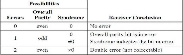
Table 2.4.1 Parity Check
Table 2.4.1 is about the possibility of the parity checks whether the parity is
even or odd by calculating how many values ‘1’ is contains in certain data.
2.5 Memory
Dynamic Random Access Memory, DRAM is the most common memory
was found in compatible personal computers, PC and workstations. DRAM is the
first released by Intel. DRAM contains of a capacitor and transistor. These cells must
be refreshed with new electricity for every few milliseconds allowing the memory to
keep its charge and hold the data as long as needed. DRAM is a volatile memory and