Design of Wideband Low Noise Amplifier using
Negative Feedback Topology for Motorola
Application
A. Salleh
1, M. Z. A. Abd Aziz, M. H. Misran, M. A. Othman, N. R. Mohamad
Center for Telecommunication Research and Innovation (CeTRI),Faculty of Electronic & Computer Engineering Universiti Teknikal Malaysia Melaka (UTeM), Malaysia
1
Abstract—This paper describes the design of wideband low noise amplifier (LNA) for Motorola application which targeted to be applied in two-way communication mobile system architecture. The technical specification was deduced from the TIA-603C standard receiver system sensitivity and inter-modulation. The proposed LNA exhibit low power consumption and adopts a negative feedback wideband amplifier topology, operated from 100 MHz to 1 GHz which covers the whole Land Mobile FM Communication Equipment (136 – 941 MHz) frequency band. The proposed topology solve the RF tracing problem inherited in the targeted frequency and also the problem of economically impractical PCB size rendered by other wideband amplifier methods. The Advanced Design System software is used to perform the simulations. The measured result show the proposed LNA using FR4 board has a stable gain of more than 15 dB, noise figure less than 1.5 dB, S11 and S22 less than -10 dB, with current consumption of 8 mA from voltage supply at 1.8 V.
Index Terms—LNA, negative feedback, wideband.
I. INTRODUCTION
ODAY, the wideband amplifier design remains one of the
most challenging portions in the communication system. The conventional low noise amplifier operates on a single band, in which it is easier to design the amplifier to meet the entire specified goal. However, MOTOROLA wideband low noise amplifier which operate from 100 MHz to 1 GHz, making it harder to design as to operate at wider spectrum while maintaining low noise < 1.5 dB, great input and output return loss <-10dB, good gain > 15 dB with reverse isolation of < -20 dB with restriction of low power consumption < 1.8 V and < 10 mA, thus presenting a tougher challenge for the designer to achieve the goals for the extended frequency range. Traditional methods of tuning and tweaking will require more tedious and time consuming effort to cover the wider frequency range, thus rendering the methods to be impractical. Therefore, a more specific technical approach must be utilized to help the designers to better design the broadband amplifier.
Portable two ways radio size has been shrinking over time, the employ of multiband radios which consist of several narrow band discrete circuits are larger because inside of housing must contain two or three separate transceivers.
Besides, driving a slightly larger housing is the additional filtering and shielding between the transceivers in order to avoid the interfering effect between different transceivers [1]. To solve this problem, the combination of several narrow bands LNA circuit into single wideband LNA circuit is proposed. Wideband LNA design presents a considerable challenge, as we know conjugate matching will give maximum gain only over relatively narrow bandwidth, while designing for less max gain will improve the gain bandwidth, but the input and output part of the amplifier will be poorly matched [2]. For this reason feedback technique is proposed to simultaneously achieve improvement in bandwidth and also on its gain, noise figure and return loss. The conventional LNA suffer from the problem that the input matching network can be tuned for low noise figure or low VSWR (conjugate transistor to transistor and furthermore, in-band stability is also improved by employing negative feedback [4].
The low noise amplifier is most important block in any receiving system because the receiving system sensitivity is generally determined by its gain and noise figure. Most of the high frequency LNAs, such as L-band, X-band, Ku-band LNAs are designed in GaAs, CMOS, JFET, PHMET and MESFET technologies. At the same time, low voltage, low power, ability to operate over a wide temperature range and better performances are always the design targets [5]. There is wide range of options on designing an LNA; it can be either single ended or differential and it can also be single stage or multistage, depending on type of application and specifications. For every design options there are advantages and disadvantages. For instance the single ended architecture has one disadvantage that it is very sensitive to parasitic ground inductance. A differential LNA can solve this problem but with differential LNA, the noise figure is higher than single ended design option [6]. A multi stage LNA will provide higher gain but the problem is that it is difficult to maintain stability than single stage LNA. The trade-offs are not avoidable. The selection of design option depends on type of application and specific design goals.
In the literature, most of the LNAs are designed using inductive degeneration architecture. For every different frequency of operation and technology the load, stability, biasing and matching networks are slightly different. Also to reach better performance such as low power, low noise, high gain and more stability, there are more techniques available. It is seen that there has been a change in trend towards designing a low noise amplifiers in last few years using CMOS, Bipolar, GaAs FET technologies. Table 1 gives recent developments in low noise amplifier technologies.
In this paper, the major goal is to design, simulate and fabricate the wideband LNA using negative feedback topology for Motorola application. The LNA design was operated from 100 MHz to 1 GHz. The performance of design can be examined in terms of gain, input and output return loss.
TABLE 1 Comparison of reported LNA with other LNA design
Reference Frequency
The technical specifications and the methodology of LNA design was explained in this section.
A. Technical Specifications
From the TIA-603C standard compliances [13], based on the radio receiver specifications, a tabulated data for all individual substations in the receiver system is shown in Table 2. There are two LNAs in the specifications for the whole radio receiver system. Since LNA2 is a second stage Intermediate Frequency (IF) amplifier and not in the Receiver Front End (RXFE), hence only LNA1 will be describe in this paper. LNA1 has a significant contribution in determining the receiver sensitivity as well as the actual RF frequency application. The frequency range is chosen based on the TIA-603C standard. Those frequency include 136MHz - 174MHz, 217MHz - 224MHz, 381MHz - 519MHz, 766MHz - 774 MHz, 851MHz – 869 MHz and 935MHz - 940 MHz [14]. The wideband LNA is required to be in single stage, low power consumption, minimum components and easily mass produced in minimum cost. The technical requirements of the proposed design are shown in Table 3.
TABLE 2 Typical RXFE system specifications for TIA-603C Compliance
TABLE 3 Specifications of LNA
Parameter Value
Operating Frequency (MHz) 100 – 1000
Noise figure (dB) < 1.5
Gain (dB) > 15
Input Third Order Inception, IIP3 (dBm) > 5
Stability Factor (K) > 1
Current (mA) < 10
Voltage (V) < 1.8
Input and Output Return Loss (dB) < -10
Figure 1. Block Diagram of LNA
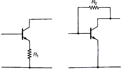
BJT technology is selected to design the wideband low noise amplifier due to its higher gain at low power consumption, with reasonable low noise figure. The most common technique in applying feedback is to have a series or shunt resistor configuration as shown in Figure 2. The BJT can be represented by the equivalent circuit in Figure 3. The resulting negative feedback equivalent network (with both series and shunt feedback) is shown in Figure 4 [4].
Figure 2. BJT with series and shunt feedback resistor
Figure 3. BJT equivalent network
Figure 4. BJT negative feedback model
The admittance matrix for the circuit model shown in Figure 4 can be written as:
By converting the y parameters of (1) to S parameter yield [15]:
and
where
From (2), the conditions are satisfied when S11 = S22 = 0 are satisfied when
or
From (7), it can be observed that with positive value of R1 and large value for transconductance value, gm, S11 = S22 = 0 can be achieved. Hence, the designer can have a range of values for R1, R2 and gm for good matching. Substituting (7) into (3) and (4) gives
and
From (7), the minimum transconductance can be achieved
while R1 = 0 ( (min) 22
o m
Z R
g ) and it follows from (8) that
For instance, in the LNA that needs to provide |S21 2
The required R2 (feedback resistor) calculated from the (7) is
Equation (8) can also be expressed as
R2 = Zo (1 + |S21|) (11)
From (11), it is noticeable that depend only on the value of and none of the transistor S-parameters, thus gain flattening can be achieved by utilizing the negative feedback technique [2]. Another consideration in the feedback design is at certain frequency, the phase of S21 will sometimes have a portion where the output voltage will in phase with the input voltage, and to prevent the positive feedback, an inductor is often added in series with R2 to decrease the feedback phase as to ensure the feedback is always negative.
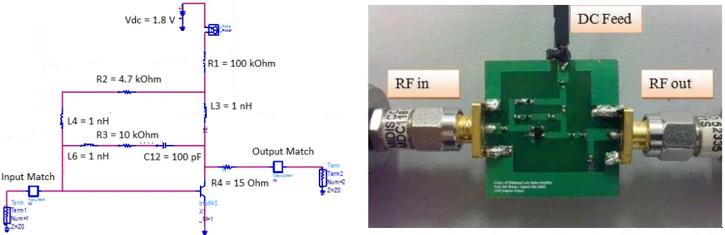
Among several topologies that provide a gain over a wideband, the RC feedback is one of the most popular techniques to be used in amplifiers circuit for its wideband input match and good linearity. The schematic of the LNA is shown in Figure 5. The transistor SPICE model is used in the schematic for simulation purpose. The transistor is self-biased with the biasing resistor of R1 and R2 at VCE =1V and IC = 8mA as the LNA is designed for low power product application. The LNA design has implemented RLC feedback in order to lower the gain at the lower frequencies and hence improve the stability of the circuit. The RLC feedback is initially set to 1000Ω, 47nH and 100pF respectively where tuning and optimization are then performed in order to meet the design specifications. The LNA design also employs output resistive loading in stabilizing the circuit. The initial output resistor value, R4 is set to only 15Ω because high output resistor value may result in huge decrease of gain and P1dB point. L3 and L4 in the circuit acts as the RF choke which blocks the DC current from entering the RF path. In this project, the LNA is matched using lumped element as it is simple and compact. The impedance matching networks is designed with the aid of Smith chart tools from ADS. Typical LC matching network include the use of capacitors and inductors in either series or shunt configuration
Figure 5. LNA schematic
III. RESULT AND ANALYSIS
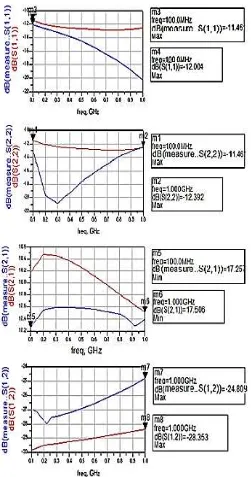
The fabricated wideband LNA is shown in Figure 6. The layout of the board was designed using the Advance Design System (ADS). The circuit is supplied with a 1.8V DC through the DC pins at the top of the board. The drain current is measured to be around 8 mA, thus it is consistent with the simulated circuit. SMA connectors are attached at both RF input and output. The fabricated board is measured using standard RF equipment such as network analyzers, signal generators, spectrum analyzer and noise figure analyzer. The simulated and measured S-Parameter performances are shown in Figure 7, while the simulated and measured NF performances are shown in Figure 8. Finally, the simulated and measured IIP3 performances are shown in Figure 9.
The most important observation of the result is that the LNA is meeting the design specification for the frequency range of interest, 100 MHz to 1 GHz. The LNA able to achieve gain, more than 17dB, and below -10dB
with below -24dB and noise figure less than 1dB. Apart from that, the K-factor of the design has been measured to be greater than 1 in both the simulated and fabricated board. This shows that the feedback LNA not only can meet the design specifications, it is also unconditional stable over the frequency of operation. The design also manage to get 1mA of current consumption.
By referring to the result, it can be observed that the simulated and measured return losses are below -10dB which indicates that the board is well match at the input. The good matching at the input ensures a good noise figure performance. The output return loss, S22 seems to resonate at 0.3GHz compared to the flat response of the simulation. The measured and simulated gain has the difference of 0.8 dB at lower frequency and the difference gets smaller at higher frequency. This shows that there is a good correlation between the simulated and actual board at higher frequency. The difference in gain is due to the parasitic effect of the components. In the simulation, parasitic effect of the component and RF traces are not taken into account. Thus, it contributes to the inaccuracy of the simulation result.
The LNA show a good reverse isolation which will prevent the signal from the output feed into input and become an oscillator. There are almost 3.5 dB different between measurement and simulated result. This is due to the miller effect if BJT transistor and the parasitic effect of the component. There are also differences of around 0.2 dB in terms of noise figure. This small difference is considered good as the noise figure of the RF board can easily be affected due to imperfect soldering, RF traces and addition of the SMA connector. The IIP3 performance also not so well correlated because at lower power, the circuit is more affected by the environmental temperature and equipment uncertainties.
Figure 7. Simulated vs Measured of S-Parameters
Figure 8. Simulated vs Measured of Noise Figure
Figure 9. Simulated vs Measured of IIP3
IV. CONCLUSION
ACKNOWLEDGMENT
The author would like to thank Universiti Teknikal
Malaysia Melaka (UTeM) for the grant number
PJP/2011/FKEKK (35C)/S00933.
REFERENCES
[1] David Lum , “Why Are Portable Two Ways Radio Larger Than
Cellphone?,” Motorola Solutions White Paper, May 2011.
[2] D. M. Pozar,“Microwave and RF Design of Wireless Systems”,3rd
Edition: John Wiley & Sons Inc, 2001.
[3] Dale D. Henkes, "LNA Design Uses Series Feedback to Achieve
Simultaneous Low Input VSWR and Low Noise," Applied Microwave &
Wireless, pp. 26, October 1998.
[4] Guillermo Gonzalez, “Microwave Transistor Amplifiers - Analysis and
Design,” Prentice-Hall, Inc., 2nd ed., 1996.
[5] Venkat Ramana. Aitha, Mohammad Kawsar Imam, “Low Noise
Amplifier for Radio Telescope at 1.42 GHz,” Master’s Thesis of
Elctrical Engineering, Halmstad University, May 2007.
[6] Xuezhen Wang, Robert Weber, “Low Voltage Low Power SiGe, BiCMOS X-band LNA Design and its Comparison Study with IEEE
802.11a LNA Design,” Conference, IEEE International, Iowa State
University, Ames, 2005.
[7] M. Cimino, H. Lapuyade, Y. Deval, T. Taris and J.B. Bégueret, ”Design of a 0.9 V, 2.45 GHz Self-testable and Reliability-enhanced CMOS LNA,” IEEE Journal of Solid-State Circuits, Vol. 43, No. 5, May 2008, pp. 1187-1194.
[8] J.Y. Hsieh, T. Wang and S.S. Lu, “Wideband Low Noise Amplifier by LC Load Reusing Technique,” Electronics Letters, Vol. 45, No. 25, December 2009, pp. 1278-1280.
[9] T.Y. Chang, J.H. Chen, L. Rigge and J.S. Lin, “A Packaged and ESD Protected Inductorless 0.1 to 8 GHz Wideband CMOS LNA,” IEEE Microwave and Wireless Components Letters, Vol. 18, No. 6, June 2008, pp. 416-418.
[10] Gramegna, G, “A sub-1-dB NF±2.3-kV ESD-protected 900-MHz CMOS LNA,” IEEE Journal of Solid State Circuits, Vol. 36. P.1010 – 1017, July 2001.
[11] Guochi Huang, “Post linearization of CMOS LNA using double cascade FETs”, Circuits and Systems, 2006. ISCAS 2006. IEEE Proceedings May 2006.
[12] Wei Guo “Noise and linearity analysis for a 1.9 GHz CMOS LNA,” Circuits and Systems, 2002. APCCAS 2002 Asia Pacific conference on Vol. 2, P.409 – 414, Oct. 2002.
[13] Motorola Solutions, “MototrboTM Digital Two-Way Radio Repeaters
Product Spec Sheet, Motorola Solutions, pp. 3-7, 2011.
[14] Guillermo Gonzalez, “Microwave Transistor Amplifiers - Analysis and
Design,” Prentice-Hall, Inc., 2nd ed., 1996.