THE DESIGN OF EMERGENCY LIGHT AND ALARM SYSTEM
KAMAL NOR AZWAN BIN KAMARUDIN
This Report Is Submitted In Partial Fulfillment of Requirement for the Degree of Bachelor in Electrical Engineering (Industry Power)
Faculty of Electrical Engineering
UNIVERSITI TEKNIKAL MALAYSIA MELAKA
UNIVERSITI TEKNIKAL MALAYSIA MELAKA FACULTY OF ELECTRICAL ENGINEERING
REPORT OF PSM ( PSM 2 )
DESIGN OF EMERGENCY LIGHT AND ALARM SYSTEM
KAMAL NOR AZWAN BIN KAMARUDIN B010510178
SUPERVISOR
PROF. MADYA DR. MUSSE MOHAMUD AHMED
“I hereby declared that I have read through this report and found that it has comply the partial fulfillment for awarding the degree of Bachelor of Electrical Engineering
(Industrial Power)”
Signature :……….
“I hereby declared that this report is of my own work except for the excerpts that have been cited clearly in the references”
Signature :……….. Name : KAMAL NOR AZWAN BIN KAMARUDIN Matric No. : B010510178
Date :………...
In the name of Allah, The Beneficent, The Merciful.
Alhamdulillah, all praise is to Allah that I have been able to complete my progress report for my Final Year Project that is The Design of Emergency Light and Alarm System.
In successfully completing this project, I would like to acknowledge my Honors‟ supervisor, Prof Madya Dr. Musse Mohamed Ahmed for his guidance and expertise that was essential to the project. I would like also to thank to my family, especially my parents, for the infinite ways in which they have supported my studies all this year. To all my friends and fellow BEKP class mates, Thanks for your support and knowledge that have helped me much going through the project. Last but not least, thanks to both my panel trough out the project for their building comments and suggestions that have helped me much in improving the project.
ABSTRACT
2.4 Calculating Load Voltage and Currents 12
2.5 Using a transistor as a switch 13
2.6 Other Emergency lights 14
CHAPTER III
PROJECT METHODOLOGY
3.1 Project Planning 19
3.2 Flow Chart 20
3.3 Hardware Design 22
3.4 Finalizing 23
CHAPTER IV
COMPONENT
4.1 Transistor 24
4.2 Rechargeable Nimh Battery (1.2V) 29
4.3 Diode 30
4.4 Buzzer 32
CHAPTER V
PROJECT DEVELOPMENT
5.1 Develop the DC Main Circuit 34
5.2 Develop the Detection Circuit 38
5.3 The overall circuit 40
5.4 The circuits or project casing 41
CHAPTER VI
6.1 Preliminary Expected Result 43
6.2 Actual result 50
CHAPTER VII
7.0 Discussion 51
7.1 Recommendations 51
REFERENCES 53
APPENDIXES 54
LIST OF TABLE
NO TITLE PAGES
Chapter III
LIST OF FIGURE
NO TITLE PAGES
Chapter II
Figure 2.1 : Full-wave rectifier circuit and waveform 5
Figure 2.2 : Diode bridge Circuit 7
Figure 2.3: The positive cycle flow 7
Figure 2.4: The negative half-cycle flow 8
Figure 2.5: The capacitors theory 9
Figure 2.6: Capacitor in open circuit 10
Figure 2.7: The resultant output waveform of bridge circuit 11 Figure 2.8: illustrates the average dc voltage for a full wave rectifier 12
Figure 2.9: Transistor switching circuit 13
Chapter III
Figure 3.1: The methodology of work flow 20
Figure 3.2: Complete system of Emergency Light And Alarm 22
Chapter IV
Figure 4.1: BJT used as an electronic switch in grounded-emitter configuration 25 Figure 4.2: Amplifier circuit, standard common-emitter configuration 25
Figure 4.3: Simple circuit using a transistor. 26
Figure 4.4 : Operation graph of a transistor. 26
Figure 4.5: BJT and JFET symbols. 28
Figure 4.6 : JFET and IGFET symbols 28
Figure 4.7: Battery 29
Figure 4.8: Symbol and picture of diode 30
Figure 4.9: LEDs symbol 31
Chapter V
Figure 5.1: Voltage waveforms 35
Figure 5.2: Types of direct current. 36
Figure 5.3: Symbol of direct current. 37
Figure 5.4: Actual rectifier circuit on PCB board 38
Figure 5.5: Developing the DC circuit using Multisim 38
Figure 5.6: Transistor switching circuit 39
Figure 5.7: The Detection circuit develop using the Multisim Software 39 Figure 5.8: The real detection circuit buzzer side on PCB. 40
Figure 5.9: The real detection circuit lamp side on PCB 40
Figure 5.10: The overall circuit connection using Multisim Software 40
Figure 5.11: The overall circuit connected on PCB 41
Figure 5.12: Upper view of the casing 42
Figure 5.13: Front View Of the casing 42
Chapter VI
Figure 6.1: Power Supply Circuit 43
Figure 6.3: Sinewave of Incoming power supply that is AC voltage. 45 Figure 6.4: Wave of voltage after passing thru the fullwave bridge diode 45 Figure 6.5: Using the light indicator to show as using emergency light 46 Figure 6.6: using buzzer to indicate the use of alarm system 47 Figure 6.7: The emergency light and alarm system full circuit 48 Figure 6.8: Show that LED 2 illuminates. This is because the circuit is charging the
battery. 48
Figure 6.9: Show the Buzzer sounded 49
APPENDIXES LIST
NO TITLE PAGE
A DATASHEET 55
B ABOUT EMERGENCY LIGHT AND
CHAPTER I
INTRODUCTION
1.1Project Overview
This project is to develop an emergency light and alarm system. As mentioned earlier, the emergency light and alarm system are already commercially available; it is the wiring system which constitutes the actual invention. This project comprises of two mains part that is the power supply circuit and the purposely-designed control circuit that includes two systems that is emergency light and alarm system. Although the project seems easy or simple, it will bring a great beneficial to human as a user. The product is developed to help humans‟ life to be more safe and easy. This product is small and light weight compare than available in market. In can easily be assemble and installed anywhere such as toilet, hallway and house because the cost of the product is considerable and affordable.
mentioned before, when a power outage occurs, the lamp automatically illuminates. Instead of illuminating a lamp, an alarm sounder can be chosen. When power supply is restored, the lamp or the alarm is switched-off. A switch provides a "latch-up" function, in order to extend lamp or alarm operation even when power is restored.
1.2 Objective Project
There are many main objective of doing this project. The main purpose of this project is to design and develop emergency light and alarm system that combines the knowledge of electrical and electronic. The main objectives of this project are:
To design the bridge diode circuit.
To understand the basic operation of circuit
To design the circuit and make the circuit operational.
Full circuit of emergency light and alarm system will be developed.
1.3Problem Statement
The inspiration behind the invention of this emergency light and alarm system being made aware of situations where blackouts and power outage have caused death. This is because power outage happen under many causes such as fire or short circuit. Some cases those deaths may have been prevented if the building occupants had had an emergency light or an alarm system to make it easier to evacuate the building.
This emergency light and alarm system is designed to avoid problems such as blackout. It will give some eyesight for the people to go to exit door in case of emergency or to avoid mishap like crashing with thing on floor. An alarm sounder can be chosen to tell someone power outage situation. Moreover, the emergency light system is a bit expensive for ordinary use such as for home use and does not included and alarm system.
1.4 Scope of the Project
To design the circuit and combine multiple theory to create an Emergency light and alarm system:
Fullwave bridge diode Smoothing capacitor
Forward and reverse bias of bipolar Junction Transistor
CHAPTER II
LITERATURE REVIEW
This chapter will discuss the literature review according to the Electrical circuit and electronic devices that are usually studied by UTeM students. It will also include all the knowledge and information while developing this project. The information is from websites, books, journals and articles. It also includes the differences between other emergency light projects.
2.1 Rectifier
There are 2 types of circuit that will produce full-wave rectification: Full-wave Rectifier
Bridge Rectifier.
In this project, bridge rectifier is chosen as part of the circuit. The explanation of full-wave rectifier and bridge rectifier will be discussed in this chapter.
2.1.1 Full-wave Rectifier
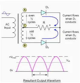
Figure 2.1 : Full-wave rectifier circuit and waveform
The circuit consists of two Half-wave rectifiers connected to a single load resistance with each diode taking it in turn to supply current to the load. When point A is positive with respect to point B, diode D1 conducts in the forward direction as indicated
by the arrows. When point B is positive (in the negative half of the cycle) with respect to point A, diode D2 conducts in the forward direction and the current flowing through
resistor R is in the same direction for both circuits. As the output voltage across the resistor R is the sum of the two waveforms, this type of circuit is also known as a "bi-phase" circuit.
As the spaces between each half-wave developed by each diode is now being filled in by the other diode the average DC output voltage across the load resistor is now double that of the single half-wave rectifier circuit and is about 0.637Vmax of the peak
The peak voltage of the output waveform is the same as before for the half-wave rectifier provided each half of the transformer windings have the same root mean square (RMS) voltage value. To obtain a different DC voltage output different transformer ratios can be used, but one main disadvantage of this type of rectifier is that having a larger transformer for a given power output with two separate windings makes this type of circuit costly compared to a "Bridge Rectifier" circuit equivalent.[1][5]
2.1.2 The Bridge Rectifier
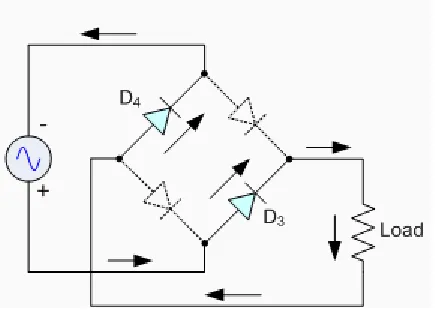
Figure 2.2: Diode Bridge Circuit
The 4 diodes labeled D1 to D4 are arranged in "series pairs" with only two diodes
conducting current during each half cycle. During the positive half cycle of the supply, diodes D1 and D2 conduct in series while diodes D3 and D4 are reverse biased and the current flows through the load as shown below.
Figure 2.3: The positive cycle flow
Figure 2.4: The negative half-cycle flow
As the current flowing through the load is unidirectional, so the voltage developed across the load is also unidirectional the same as for the previous two diode full-wave rectifier, therefore the average DC voltage across the load is 0.637Vmax and
the ripple frequency is now twice the supply frequency (e.g. 100Hz for a 50Hz supply).[1]
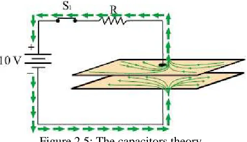
2.2 Basic Theory for capacitor as a filter
plate and gather on the lower plate. This creates a sudden high current as the electrons rush through the power supply to change plates. Remember that electrons repel each other. As more and more electrons collect on the lower plate, they are forced closer together. This causes a reverse pressure to build as more and more electrons are forced into the plate. As the reverse pressure builds, the current flows slow down and stops when the reverse pressure is equal to the power supply voltage. Now the upper plate is positive and is deficient in electrons and the lower plate is negative and has an n excess in electrons.
Figure 2.5: The capacitors theory