An Evaluation of 2-phase Charge Pump Topologies
with Charge Transfer Switches for
Green Mobile Technology
Yan Chiew Wong1,2, Nurul H. Noordin1,2, Ahmed O. El-Rayis1,2, Nakul Haridas1,2, Ahmet T. Erdogan1, Tughrul Arslan1,2
1
Institute of Integrated Micro and Nano Systems, School of Engineering, The University of Edinburgh, EH9 3JL, UK
2
Advanced Smart Antenna Technologies Research Group, School of Engineering, The University of Edinburgh, EH9 3JL, UK {Y.Wong, N.Noordin, A.El-Rayis, N.Haridas, A.Erdogan, T.Arslan}@ed.ac.uk
Abstract- The development of charge pumps has been motivated by the power supply requirements of portable electronic devices. Charge pumps are inductorless DC-DC converters that are small size and high integration. The quality of the charge pump greatly depends on the effectiveness of switches to turn on and off at the designated clock phases. However, to date, no analysis has been carried out on the overall performance of charge pumps based on switch components in practice. This work demonstrates the characteristics of transistors as charge transfer switches and their effects on the performance of a charge pump. Three most common charge pump topologies are evaluated in terms of voltage drop due to on-resistance and charge loss per switch. Simulations are performed in 0.35µm
Austriamicrosystems (AMS) technology for Dickson, Voltage Doubler and Makowski charge pump topologies in steady and dynamic states. In addition, the effect of switch parameters for different charge pump topologies are compared and analysed. We demonstrate that the Makowski charge pump is the topology for future green mobile technology.
Keywords –Charge Transfer Switch; Charge pumps; DC-DC Converter; Green Mobile Technology
I. INTRODUCTION
A charge pump is an inductorless DC-DC converter that uses only capacitors and switches without involving amplifiers or transformers to step up or step down the voltage. This approach has the advantages of a simple control method, reduced physical volume, less electromagnetic interference (EMI), low cost and high power density for its design. A charge pump is a device of choice in a portable appliance where the normal range of operating voltages is limited and it provides the ability for System-on-Chip (SoC) integration with various other devices and components when the application dictates. Among various types of charge pumps, the 2-phase charge pump appears as one of the most promising topology due to its simpler switching circuitry when used in mobile technology. Extensive studies of charge pumps have been performed but most of these treat switches as ideal components [1-3]. Understanding the behavior of switches in the respective charge pump topologies is crucial in order to have a greener technology implementation. However, very few papers have discussed the effect of switches and those discussions referred to only one charge pump topology [4-7]. Up till now, no comparison amongst
Dickson, Voltage Doubler and Makowski charge pumps has been made from the point of view of the switches. This paper presents a comprehensive study on the behavior and selection of switches, as well as evaluating transistor parameters in a steady and dynamic state for various charge pump topologies.
In section II, the characteristics of switches used in various charge pumps are presented. The challenges of the implementation of n channel (nMOS) and p channel transistors (pMOS) in charge pumps are discussed in section III. The parameters of transistors are evaluated in steady and dynamic state in section IV. The evaluated equations are validated with the simulation results.
II. SWITCHES USED IN VARIOUS TOPOLOGIES OF 2 PHASE
-CHARGE PUMPS
Most topologies of charge pumps are based on three types: The Dickson, cross-connected Voltage Doubler and Makowski. Dickson charge pump is one of the DC-DC converters used in mixed mode circuits to generate the required high voltages through cascade connection of a suitable number of identical stages (N) to give an output voltage equal to (N+1)*VDD[8]. High voltage transistors are used in the Dickson charge pump to prevent excessive gate oxide stress [5, 9]. High voltage transistors lead to a large gate area and parasitic capacitance with their high threshold voltage (VTH) compared to low voltage devices.
Makowski introduced an N-stage charge pump with its final voltage gain limited by (2N+1)th Fibonacci number
(F(N+1) ) [2, 3, 6, 11]. This gain is the maximum conversion
ratio that can be attained from a 2-phase switch capacitor charge pump by using N-1 capacitors. However, a high voltage of clock amplitude (VCLK) i.e. 0V to F(N+1)*Vin is used to maintain the voltage gain multiplication per stage. Thus, high voltage transistors must be used in this topology to avoid transistor gate oxide break down.
III. TYPES OF SWITCHES
The first charge pump was designed using diodes as charge transfer switches which had a low voltage gain per stage resulted from the high voltage drop across diode VD [12-14]. In later stages, MOSFETs which have a better switching feature are used to replace diodes as charge transfer switches in the charge pumps.
In designing the charge pump, MOSFETs have to operate in the linear region to transfer a high current with a small on-resistance [6, 15]. An energy efficiency charge pump is determined by the effectiveness of MOSFETs in turned on and off at the designated clock phases. However, both nMOS and pMOS have difficulties in switching on and off. nMOS can be easily switched off by applying a gate voltage of 0V or an effective gate to source voltage (VGS_eff) smaller than the
VTH [15, 16]. However, to switch on the nMOS without suffering from significant voltage drop, the VGS_eff of the nMOS has to be higher than VDD after deducting the VTH [12, 15]. The VTH increases when the bulk’s potential, VB, is
applied [16]. The performance of nMOS as a charge transfer switch also deteriorates with body effect. In the design of low conversion ratio charge pump, the bulk of the nMOS is grounded. However, with the scaled down gate voltage, a higher conversion ratio is required. The transistor may break down when the potential between the drain or the source or the gate terminal (VD/S/G)and VB is greater than the technology specific voltage. Thus, in the design of higher conversion ratio charge pump, the bulk of the nMOS transistor is connected to the lower terminal between the drain and the source [10]. The voltages of the source and the drain terminal will increase with the increased stages of charge pump. Thus, a higher VTH will be generated at the higher stages. This will lead to body effect [16, 17]. In this condition, the transconductance (gs) between the source and the bulk as shown in (1) can no longer be ignored. For MOSIS technology 0.8µm, while the source to bulk voltage (VSB)
reaches above 15V with VTH0 of 0.08V, the actual VTH
exceeds 2.5V [13]. This body effect seriously diminishes the output voltage of the charge pump. As the stage of charge pump increases, the overall VTH increases as well and this decreases the voltage gain per stage. To reduce the VTH
dependence on the stages, boosted pump clock schemes were introduced [5, 17].
where VTH0n/pis the threshold voltage with zero VSB of nMOS or pMOS, gs is the transconductance between the source and the bulk, VGS_eff=VGS_CLK-αNVTH0n/p, VGS_CLK is the amplitude of the switching clock, α is the coefficient proportional to the number of stages of the charge pump with the values between 0<α<1 and N is the number of stages of charge pump
For the charge pump using pMOS switches, this type of transistor can easily be switched on by VGS_eff= 0V. However, they have problems with completely switching off the pMOS switches. To avoid leakage current from the drain or the source to substrate, the bulk of pMOS should be connected to the highest terminal. Normally, it will be tied at the highest potential either the source or the drain. However, while pMOS in charge pump topology, the potentials of the drain and the source of pMOS are not always maintain at the highest. Thus, pMOS switches suffer from determining the highest potential terminal. Auxiliary transistors were used to ensure the bulk of pMOS is always connected to the highest potential between the drain and the source [12, 15, 17, 18].
IV. ANALYSIS OF STEADY STATE SWITCHES IN CHARGE
PUMPS
At steady state, the switches are operating in the linear region. To determine the general on-resistance [16] per switch in charge pumps, VGS_effplays a significant role as shown in (2). The VGS_eff can be calculated based on the amplitude of switching clock (VCLK) minus the multiply of coefficient (α) and threshold voltage with zero VSB (VTH0). The α is proportional to the number of stages of the charge pump with the values at between 0 and 1. and the width of the transistor, VGS_eff is the effective gate to source voltage, COXis the gate oxide of the transistor, λ is the output impedance constant andµnis the mobility of electrons.
The VGS_efflimits the number of stages in the charge pump.
The amplitude of the switching clock (VCLK) depends on charge pump topologies. For the Dickson and the cross-connected charge pumps, VCLK varies from 0V to VDD. While for the Makowski charge pump, the VCLK swings between 0V
charge pump with N+1 nMOS-type switches is shown in (3). While for the Voltage Doubler and Makowski charge pumps, their average on-resistances can be determined from (4) and (5) respectively. N numbers of nMOS and 2N+1 pMOS transistors are used in Makowski charge pump. The topology of Voltage Doubler charge pump requires the highest switches with 2N of nMOS and 2N of pMOS transistors.
where Ravg is the average on-resistance, VGS_effniand VGS_effpi
are the effective gate to source voltages applied to ith of nMOS and pMOS respectively in the N number of stages of charge pump, λn is the output impedance constant,µn/pis the mobility of electrons/hole, Coxn/p, Ln/pi, Wn/pi are the gate oxide capacitance, the length and the width for ith of nMOS and pMOS respectively.
V. SIMULATION RESULTS
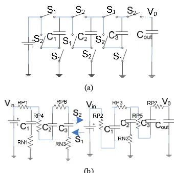
Three different charge pump topologies were simulated in Advanced Design System 2009 based on 0.35µmCMOS technology. To have an equal comparison, all charge pumps were simulated on their best performance setting. Width of nMOS and pMOS, charge storage capacitances (C) and output capacitance (Cout) were set at their respective optimum values based on previous research works [5, 6, 10, 13], while length of nMOS and pMOS were set slightly higher than the minimum channel length i.e. 0.5µm. Three of the charge pumps were driving the same load of output impedance. By using similar output impedance for these three charge pumps, their output currents were fixed and the voltages will be evaluated. The charge pumps were switched on and off by two non-overlapping S1 and S2 with the VDD
amplitude of 3.7V. The measurement of the voltage drop across respective switches was performed in steady state, where the dynamic loss can be neglected. The steady state of the switches with an approximately similar number of components used in Dickson, Voltage Doubler [14] and Makowski charge pumps are shown in Fig. 1, 2 and 3 respectively. In the figures, the RN and RP are representing the on-resistance in nMOS and pMOS respectively in steady state.
Fig. 4 shows the simulation results of the average voltage drop due to on-resistance in respective switches of different charge pump topologies. All of the charge pump topologies have half of their total on-resistance switches operated in
each clock cycle. In terms of the values of on-resistance per switch, Makowski topology has the lowest on-resistance with its high VGS_eff and W/L ratio. For the Voltage Doubler, cross-connected structure leads to transistors operating in the linear to weak region. Low VGS,eff results in slightly higher on-resistance, however, this topology is designed for low voltage transistors [10] with lower VTH, thus in practice a lower voltage drop can be obtained. Dickson charge pump shows the highest voltage drop per switch in the higher stages due to its weaker VGS,eff.
(a )
(b)
Fig. 1 Dickson charge pump (a) Topology (b) Switches in steady state
(a)
(b)
Fig. 2 Voltage Doubler charge pump (a) Topology (b) Switches in steady state
(a)
(b)
RP4
RN1 RN2 RN3 RN4
RP4
Dickson Voltage Doubler Makowski
Fig. 4 Voltage drop of 2-phase charge pumps by switches in steady states
VI. ANALYSIS OF DYNAMIC STATE SWITCHES IN CHARGE
PUMPS
In a dynamic state, the main charge loss in switches is due to the gate capacitances and drain/source bulk capacitances as shown in (6) and (7). and drain/source to bulk capacitances respectively, Wn/p and
Ln/p are the width and length of nMOS and pMOS transistors,
COX is the gate oxide capacitance, Cj and Cjsw are the junction capacitances
The Ln/p, Cj, Cjsw and Cox are typically the parameters that can be found in the technology specified. Since Ln/p of the transistor in the charge pump is much smaller than Wn/p, then by simplifying (7) and (6), the total charge loss per switch is developed in (8).
eff
Thus, the total charge loss in switches is proportional to Wn/p
and the VGS_eff of the transistor.
Fig. 5 shows the total charges consumed by each switch based on different optimized design specifications of charge pump topologies [5, 6, 10, 13]. In these three topologies, the Voltage Doubler shows the lowest charge consumed per cycle due to its narrow channel transistor compared to the others. However, the Voltage Doubler operates at a higher frequency compared to the Dickson and Makowski topologies. Thus, it will eventually accumulate a higher charge loss. Makowski charge pump topology uses higher
VGS_eff and greater width of transistor compared with the
Dickson charge pump to accommodate the high volume of charge transfer per clock cycle. Thus, higher charge is consumed by switches in Makowski charge pump at dynamic state when compared with Dickson topology as seen in Fig. 5.
Dickson Voltage Doubler Makowski
10
Fig. 5 Total charge loss of charge pumps by switches in dynamic states
VII. CHARGE PUMP FOR GREEN MOBILE TECHNOLOGY
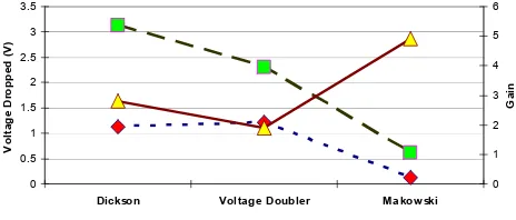
The Dickson charge pump demonstrates the highest total voltage loss in these three topologies as shown in Fig. 6. High voltage loss is not an option for mobile technology where high energy will be consumed in portable devices. The Voltage Doubler having the intermediate voltage dropped but exhibits the lowest voltage gain in this simulation. More transistors and capacitors are needed to generate the higher conversion ratio. Consequent of using higher stages, higher losses will accumulate in the charge pump. From a green technology point of view, the Makowski charge pump demonstrates the lowest voltage loss in a steady state due to large ratio of W/L.
Even though Makowski topology shows a higher dynamic switches loss, the resulted voltage loss from the dynamic state is relatively low compared to the steady state. Makowski charge pump exhibits the lowest voltage loss either for overall total voltage or voltage dropped per gain in obtaining the highest conversion ratio. Thus, by applying Makowski charge pump topology, a smaller chip area can be achieved for a higher voltage gain without sacrificing the converter size, which is critical for green portable applications.
0
Dickson Voltage Doubler Makowski
V
Total voltage dropped in Switches Total Voltage dropped per gain Voltage Gain
VIII. CONCLUSIONS
An analysis on switches applied in different charge pump topologies from the green technology perspective is presented. The nMOS and pMOS require a proper magnitude
of VGS_eff for effectively turned on and turned off at the
designated clock phases to functions as charge transfer switches. Lower on- resistance at the steady state can be obtained by using higher VGS_eff and W/L ratio. However, greater W of the transistor will cause to higher charge loss in dynamic state. The Dickson charge pump consumes the most voltage loss in a steady state while the Voltage Doubler generates the lowest conversion ratio for an approximately similar number of switches. This work reveals that the Makowski charge pump is the best model for green technology as it provides the lowest voltage dropped in the topology targeting for the highest voltage gain.
ACKNOWLEDGMENT
The authors would like to thank the SOFANT engineering team for their help and support in this work. The authors gratefully acknowledge the financial support from Universiti Teknikal Malaysia Melaka, Univerisiti Malaysia Pahang and Malaysia Government.
REFERENCES
[1] J. A. Starzyk, J. Ying-Wei, and Q. Fengjing, "A DC-DC charge pump design based on voltage doublers," IEEE Transactions on Circuits and Systems I: Fundamental Theory and Applications, vol. 48, pp. 350-359, 2001.
[2] K. Chi-Wah, W. Oi-Ying, T. Wing-Shan, and W. Hei, "Design strategy for two-phase switched capacitor step-up charge pump," IEEE International Conference of Electron Devices and Solid-State Circuits, EDSSC 2009., 2009.
[3] M. S. Makowski, "Realizability conditions and bounds on synthesis of switched-capacitor DC-DC voltage multiplier circuits," IEEE Transactions on Circuits and Systems I: Fundamental Theory and Applications, vol. 44, pp. 684-691, 1997.
[4] Y. Hairong and C. Zhiliang, "A two-phase, four and five boosting ratio, charge pump cell for LCD driver," 4th International Conference on ASIC, 2001, 2001.
[5] A. C. Davide Baderna, Marco Pasotti, Guido Torelli, "Power Efficiency Evaluation in Dickson and Voltage Doubler Charge Pump Topologies," Microelectronics Journal pp. 1128-1135, 2006.
[6] L. Lifang and C. Zhiliang, "Analysis and design of Makowski charge-pump cell," 6th International Conference On ASIC, 2005. ASICON 2005. , 2005.
[7] T. Tanzawa and T. Tanaka, "A dynamic analysis of the Dickson charge pump circuit,", IEEE Journal of Solid-State Circuits, vol. 32, pp. 1231-1240, 1997.
[8] P. Favrat, P. Deval, and M. J. Declercq, "A high-efficiency CMOS voltage doubler," IEEE Journal of Solid-State Circuits, vol. 33, pp. 410-416, 1998.
[9] K. Ming-Dou, C. Shih-Lun, and T. Chia-Shen, "Design of charge pump circuit with consideration of gate-oxide reliability in low-voltage CMOS processes," IEEE Journal of Solid-State Circuits, vol. 41, pp. 1100-1107, 2006.
[10] R. Pelliconi, D. Iezzi, A. Baroni, M. Pasotti, and P. L. Rolandi, "Power efficient charge pump in deep submicron standard CMOS technology," IEEE Journal of Solid-State Circuits, vol. 38, pp. 1068-1071, 2003. [11] S. V. Cheong, H. Chung, and A. Ioinovici, "Inductorless DC-to-DC
converter with high power density," IEEE Transactions on Industrial Electronics, vol. 41, pp. 208-215, 1994.
[12] S. Feng, K. Wing-Hung, and T. Chi-Ying, "Gate control strategies for high efficiency charge pumps," IEEE International Symposium on Circuits and Systems, 2005. ISCAS 2005. , 2005.
[13] T. S. Feng Pan, Charge Pump Circuit Design: McGraw-Hill, 2006. [14] J. F. Dickson, "On-chip high-voltage generation in MNOS integrated
circuits using an improved voltage multiplier technique," IEEE Journal of Solid-State Circuits, vol. 11, pp. 374-378, 1976.
[15] W. Oi-Ying, T. Wing-Shan, K. Chi-Wah, and W. Hei, "A novel gate boosting circuit for 2-phase high voltage CMOS charge pump," IEEE International Conference of Electron Devices and Solid-State Circuits, 2009. EDSSC 2009. , 2009.
[16] K. M. David A. Johns, Analog Integrated Circuit Design: John Wiley & Sons, Inc., 1997.
[17] W. Jieh-Tsorng and C. Kuen-Long, "MOS charge pumps for low-voltage operation," IEEE Journal of Solid-State Circuits, vol. 33, pp. 592-597, 1998.