DESIGN AND DEVELOPMENT OF SWITCHABLE MATCHED BANDSTOP TO BANDPASS FILTER USING RING RESONATOR
NURUL AINI BINTI AMRAN
This Report Is Submitted In Partial Fulfilment of Requirement for the Bachelor Degree of Electronic Engineering (Wireless Communication)
Faculty of Electronics and Computer Engineering
Universiti Teknikal Malaysia Melaka
ii
UNIVERSTI TEKNIKAL MALAYSIA MELAKA
FAKULTI KEJURUTERAAN ELEKTRONIK DAN KEJURUTERAAN KOMPUTER
BORANG PENGESAHAN STATUS LAPORAN
PROJEK SARJANA MUDA II
Tajuk Projek : DESIGN AND DEVELOPMENT OF SWITCHABLE MATCHED BANDSTOP TO BANDPASS FILTER USING RING RESONATOR
…
Sesi Pengajian :
Saya NURUL AINI BINTI AMRAN mengaku membenarkan Laporan Projek Sarjana Muda ini disimpan di Perpustakaan dengan syarat-syarat kegunaan seperti berikut:
1. Laporan adalah hakmilik Universiti Teknikal Malaysia Melaka.
2. Perpustakaan dibenarkan membuat salinan untuk tujuan pengajian sahaja.
3. Perpustakaan dibenarkan membuat salinan laporan ini sebagai bahan pertukaran antara institusi pengajian tinggi.
4. Sila tandakan ( √ ) :
SULIT*
*(Mengandungi maklumat yang berdarjah keselamatan atau kepentingan Malaysia seperti yang termaktub di dalam AKTA RAHSIA RASMI 1972)
TERHAD** **(Mengandungi maklumat terhad yang telah ditentukan oleh
organisasi/badan di mana penyelidikan dijalankan)
TIDAK TERHAD
Disahkan oleh:
__ ________________________ ___________________________________ (NURUL AINI BINTI AMRAN) (PM. DR. BADRUL HISHAM BIN AHMAD)
“I hereby declare that the work in this project is my own except for summaries and quotations which have been duly acknowledge.”
Signature : ...
Author : NURUL AINI BINTI AMRAN
iv
“I acknowledge that I have read this report and in my opinion this report is sufficient in term of scope and quality for the award of Bachelor of Electronic Engineering (Wireless
Communication) with Honours.”
Signature : ...
Supervisor’s Name : PM. DR. BADRUL HISHAM BIN AHMAD
ACKNOWLEDGEMENT
Firstly, I would like to convey my deepest appreciation to my Bachelor Degree Project Supervisor, PM. Dr. Badrul Hisham Bin Ahmad for taking some of his precious time to evaluate my Bachelor Degree Project report as well as helping and supporting me throughout my project implementation at Universiti Teknikal Malaysia Melaka (UTeM). Thank you as well for giving me constant guidance and corrective advices all the while I was carrying out this final year project.
Secondly, I would like to thank the panels, lecturers and staffs of UTeM for assessing, evaluating and assisting me directly or indirectly for the PSM 1 and PSM 2 seminars, iNOTEK competition as well as for my fabrication process for the prototype of this project.
Furthermore, I would like to express my utmost gratitude to Mr. Mohd Khairy Bin Zahari, a PhD student in UteM for his consistent help and advice in developing my skills and knowledge besides giving me so many helpful guidance the whole time I was undergoing this Bachelor Degree Project.
vi
ABSTRACT
viii
ABSTRAK
TABLE OF CONTENTS
1.1 PROJECT INTRODUCTION 1.2 PROBLEM STATEMENT 1.3 OBJECTIVE
1.4 SCOPE
1.5 SIGNIFICANCE OF PROJECT DESIGN
x
2
3
1.6 BRIEF OVERVIEW ON THE METHODOLOGY OF THE PROJECT
1.7 THESIS SCOPE
LITERATURE REVIEW
2.1 FUNDAMENTAL OF MICROWAVE FILTERS 2.1.1 Conventional Bandstop Filters
2.1.2 Conventional Bandpass Filters
2.1.3 Applications of RF and Microwave Filters 2.2 THEORY OF MATCHED BANDSTOP FILTERS 2.3 DESIGN OF MATCHED BANDSTOP FILTERS USING LOW-Q RESONATORS
3.1 FUNDAMENTAL RESEARCH
3.1.1 Fundamental of the Filter Design 3.2 DESIGN AND SIMULATION
4
4.1 DESIGN AND SIMULATION RESULTS 4.1.1 First Schematic Design
4.1.2 Layout Design and Second Schematic Design
4.2 FABRICATION OF THE FILTER DESIGN 4.3 MEASURED RESULTS
4.3.1 Matched Bandstop Response 4.3.2 Bandpass Response
4.4 COMPARISON BETWEEN SIMULATION RESULTS AND MEASURED RESULTS
CONCLUSION AND SUGGESTIONS
5.1 CONCLUSION
5.2 IMPORTANCE OF PROJECT DESIGN 5.3 POTENTIAL OF COMMERCIALIZATION 5.4 SUGGESTIONS FOR FUTURE WORK
xii
LIST OF TABLES
TABLE
2.1 3.1 4.1
TITLE
Design Specification of FR4 Substrate FR4 Substrate Specification
Comparison between Simulation and Measured Results
PAGE
LIST OF FIGURES
System Level Block Diagram of a Bandstop Filter Bandstop Filter Circuit
System Level Block Diagram of a Bandpass Filter Capacitive Bandpass Filter Circuit
Inductive Bandpass Filter Circuit RF Front End of a Cellular Base Station
Generalized Coupled-Resonator Model of a Matched Bandstop Filter
Hybrid Circuit Implementation of a Perfectly-Matched Bandstop Filter
Generalized Coupled-Resonator Model of a Matched Bandstop Filter
Coupled Resonator Design with the Desired Parameter for the Matching Bandstop Filter
xiv
Hybrid Circuit Implementation of a Perfectly-Matched Bandstop Filter
Generalized Coupled-Resonator Model of a Matched Bandstop Filter
Implementation of Ring Resonator Based on the Coupled-Resonator Model
Schematic Circuit Design for Matched Bandstop Filter Desired Output Response for the Matched Bandstop Filter After Tuning
Layout Design Schematic Design
Gantt Chart for Project Planning Flowchart of the Methodology Process
First Schematic Circuit Design for the Matched Bandstop tp Bandpass Filter
Matched Bandstop Response from Simulation of the Schematic Circuit Design
Layout Design
Second Schematic Design
Matched Bandstop Response from the Layour and Second Schematic Design
Bandpass Response from the Layout and Second Schematic Design
Fabricated Switchable Matched Bandstop to Bandpass Filter
Measured Matched Bandstop Response using Network Analyzer
Measured Bandpass Response using Network Analyzer
LIST OF ABBREVIATIONS
ADS Advanced Design System FR4 Flame Retardant Grade 4
RF Radio Frequency
Q Quality
MCLIN Microstrip Couple Line MLIN Microstrip Line
SMD Surface Mount Device
CHAPTER 1
INTRODUCTION
1.1 PROJECT INTRODUCTION
state). This project will present the theoretical analysis and implementation of the approach.
1.2 PROBLEM STATEMENT
As the modern wireless and microwave systems are progressing towards the spectral cognitive systems, it is necessary to produce more and more reconfigurable filter in order to enable the full potential of the system’s performance while at the same time being small-sized and low-cost product. This project aims to propose a new technique of a reconfigurable filter using dual-mode ring resonator that allows the filter to switch its operation from being a matched bandstop filter to bandpass filter where varactor diodes are added into the network topology as the switching elements. This switchable filter operates at a frequency of 1GHz, able to provide a high quality factor (above 30) and is also compact in size.
1.3 OBJECTIVE
The purpose of this project is to propose a new technique of designing a switchable matched bandstop to bandpass filter by using a dual-mode ring resonator that is able to switch the filter’s operation from being a matched bandstop filter to a bandpass filter. Therefore, for the purpose of this research, three objectives have been identified which are described as follows:
3
ii. To analyze and improve the switchable matched bandstop to bandpass filter design in terms of achieving the highest quality factor and reduced in the filter’s size as well as tuning the filter design in the simulation to obtain the best possible result before proceeding with the fabrication process.
1.4 SCOPE
The scope of this project will limit itself in designing the switchable matched bandstop to bandpass filter based on the design specifications as listed below:
i. Design of filter with the help of ADS software.
ii. Using the microstrip technology as models of fabrication. iii. The designed filter is based on a dual-ring resonator. iv. Fabrication of the filter design using FR-4 board.
v. Filter must have the ability to switch its operation from giving a matched bandstop response to a bandpass response.
vi. The operating frequency of the filter is at 1GHz.
vii. Varactor diodes are used as switching elements of the filter.
viii. The S11 response for the matched bandstop filter must be below than 15dB.
ix. The S21 response for the matched bandstop filter must be below than 20dB.
1.5 SIGNIFICANCE OF PROJECT DESIGN
There are many importance of realizing this project design. The main significance of this project design are described as follows:
i. The switchable matched bandstop to bandpass filter is a compact filter having two modes of operation in only one filter design. This means that instead of having a number of filter banks, this design reduces the complexity of the system by allowing filter re-configurability to switch from being a matched bandstop filter to a bandpass filter.
ii. The ability to produce a low cost filter that offers a high performance to the system. The switchable matched bandstop to bandpass filter uses a low cost substrate (FR-4) for fabrication. However, this design offers similar result to that of using an expensive substrate for the fabrication of the filter. iii. The ability to offer better performance compared to a conventional bandstop filter. The switchable matched bandstop to bandpass filter is more selective, does not have any reflected signal in its response, low loss and has narrower bandwidth which results in high quality factor. Compared to a conventional bandstop filter, a conventional bandstop filter is quite lossy, has reflected signal in its response which means that it does not fully attenuate the signal, and also has a wider bandwidth which results in low quality factor.
1.6 BRIEF OVERVIEW ON THE METHODOLOGY OF THE PROJECT
5 (ADS). The last part consist of the fabrication process of the designed filter onto the FR-4 board with fixed specifications and also analyzing the measured results obtained after fabrication has been done.
1.7 THESIS SCOPE
CHAPTER 2
LITERATURE REVIEW
2.1 FUNDAMENTAL OF MICROWAVE FILTERS
A microwave filter can be described as a two-port network that is used mainly to control the frequency response at a certain point in an RF or microwave system. This is done by providing transmission at frequencies which is within the passband of the filter and attenuation in the stopband of the filter. The typical frequency responses include low-pass, high-pass, bandpass and bandstop (also known as band-reject or notch) characteristics. The application of microwave filters can be found in virtually any type of RF or microwave communication, radar, or even test and measurement system.
2.1.1 Conventional Bandstop Filters
7
Figure 2.1: System Level Block Diagram of a Bandstop Filter
Figure 2.2 shows the structure of a bandstop circuit when constructed using two capacitive filter sections.
Figure 2.2: Bandstop Filter Circuit
The low-pass filter section is comprised of R1, R2 and C1 in a “T” configuration while the high-pass filter section is comprised of C2, C3 and R3 also in a “T” configuration. This arrangement is commonly known as a “Twin-T” filter, which gives sharp response when the component values are chosen in the following ratios:
R1 = R2 = 2(R3) (2.1)
C2 = C3 = (0.5)C1 (2.2)
(2.3)
2.1.2 Conventional Bandpass Filters
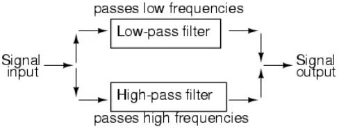
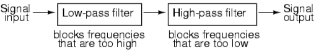
Bandpass filters are used for applications where a particular band, or spread, or frequencies are needed to be filtered from a wider range of mixed signals. A single filter comprises of a combination of low-pass and high-pass properties is called a bandpass filter. The bandpass filter circuit can be created from a low-pass and high-pass filter placed in series with each other as shown in Figure 2.3 below.
Figure 2.3: System Level Block Diagram of a Bandpass Filter
9
Figure 2.4: Capacitive Bandpass Filter Circuit
Figure 2.5: Inductive Bandpass Filter Circuit
2.1.3 Application of RF and Microwave Filters
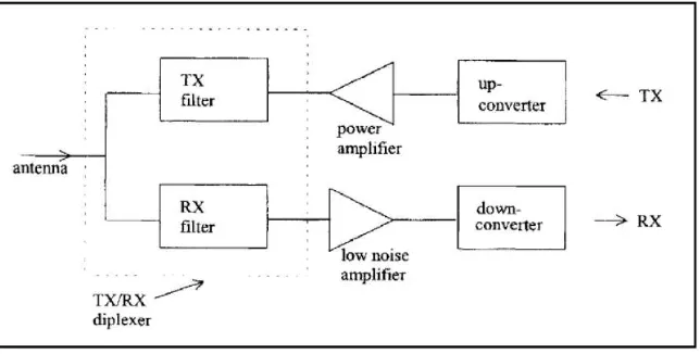
Nowadays, the modern society have been given an enormous impact by the microwave systems. Microwave systems applications are diverse. It may include any application from entertainment via satellite television, to civil and military radar systems. As conventional telephony are a widespread, the use of cellular radio systems are also increasing in the field of communications. Basically, microwave and RF filters are most widely used in all of these systems mainly to discriminate between wanted and unwanted signal frequencies. Cellular radio provides particularly demanding filter requirements both in the base stations and in mobile units. Figure 2.6 shows the block diagram of a typical filtering application which is the RF front end of a cellular radio base station.
Figure 2.6: RF Front End of a Cellular Base Station
11 order to isolate the high power transmitter. The low passband insertion loss of the transmitter allows the preservation of the system sensitivity. In summary, the selectivity of filters properties is essential to achieve base station filters with remarkable performance.
2.2 THEORY ON MATCHED BANDSTOP FILTERS
A perfectly matched bandstop filters are realized at high frequencies where the lossy nature of microstrip makes it difficult to achieve a high quality factor. In order to improve the quality factor of a bandstop limiter, a perfectly notched concept is applied in this design. The perfectly notched concept makes use of two identical lossy resonators which are coupled to a 90⁰ hybrid coupler with correct coupling factors based on the reflection mode filter. When the filer operate at the center frequency, the incident signals are critically coupled to the resonators and is absorbed into the resistive part of the resonator. This leaves no reflected signals at the output and thus achieving a theoretically infinite attenuation. A bandstop limiter is one of the most practical implementation of a lossy allpass network where the filter design implements the concept of a coupled-resonator model. The coupled-resonator model represents a matched bandstop filter based on L-shape resonator. By scaling the nodes of the admittance matrix of the 90⁰ hybrid circuits, the generalized coupled-resonator model of a perfectly matched bandstop can be obtained. Figure 2.7 shows the generalized coupled-resonator model of a matched notch filter whereas the generalized equation for the even-odd admittance of a perfectly matched bandstop filter are as follows:
Yeven (p) = -j + Ys b + jKK (2.4)
Figure 2.7: Generalized Coupled-Resonator Model of a Matched Bandstop Filter
2.3 DESIGN OF MATCHED BANDSTOP FILTERS USING LOSSY LOW-Q RESONATORS
2.3.1 Generalized Coupled-Resonator Model of a Matched Bandstop Filter
The quadrature hybrids are 3dB directional couplers with a 90⁰ phase difference in the outputs of the through and coupled arms. This type of hybrid is often made in microstrip line or stripline form and is also known as a branch-line hybrid. Figure 2.8 below shows the hybrid circuit implementation of a perfectly-matched bandstop filter.
13
Based on the 90⁰ hybrid circuit, a generalized coupled-resonator model of a matched bandstop filter is then produced as shown in Figure 2.9.
Figure 2.9: Generalized Coupled-Resonator Model of a Matched Bandstop Filter
2.3.2 Matched Bandstop Filter using L-Shape Resonator
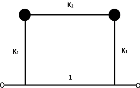
The design of a matched bandstop filter consists of two parallel-coupled half-wavelength resonators. The short transmission lines that produced a nominally-90⁰-phase shift element between the resonator couplings in a single structure. Figure 2.10 shows the transformation of the general coupled resonator model to become an L-shape resonator with the desired parameter for the matching bandstop filter.
The design of the matched bandstop filter using the L-shape resonator is based on the FR4 substrate specifications as shown below.
Dielectric Constant, εr Substrate Thickness, H Metal Thickness, T Loss Tangent, D
4.7 1.6mm 0.035mm 0.019
Table 2.1: Design Specification of FR4 Substrate
This specification is used for the reconfigurable matched bandstop filter which is designed at the center frequency of 1GHz. In order to achieve a matched bandstop response between the S11 and S21 at one resonant frequency, a perfectly notch topology with lossy resonator is implemented. K2 equals to 1 where 1 is considered as 90⁰ length. To ensure that the two modes can be overlapped with each other and achieve cancellation, the value of K1 gap will be tuned gradually to produce a notch bandstop. By adding the switching elements such as PIN diodes into the filter, the reconfigurable matched bandstop filter can be designed.
2.3.3 Matched Bandstop Filter using Ring Resonator
Based on the generalized coupled-resonator model, a dual mode design consisting of a ring resonator which is coupled with a thru line can be obtained. The dual mode design is coupled into the two modes which is 90⁰ and this will effectively set up a single wave circulating around the resonator. At resonance, the power coupled off from the resonator at the output is equal the in power and is 180⁰ out of phase with the signal that is exiting the thru-line. A perfect notch is then produced. Figure 2.11 shows the travelling wave
interpretation of the dual-mode ring resonator notch where the two modes of the
15
Figure 2.11: Travelling-Wave Interpretation of the Dual-Mode Ring Resonator Notch
The dual mode ring resonator structure consists of two degenerate modes or splitting resonant frequencies. The modes can be excited by using perturbing stubs, notches or symmetrical feed lines. The ring resonator with a perturbing stub or notch can be placed at 45⁰, 135⁰, 225⁰ or 315⁰ and can be shown in Figure 2.12.
Figure 2.12: Perturbing Stub Placed At 135⁰
modes are excited and coupled to each other if one of the half-wavelength resonator is perturbing out of balance with the other.
CHAPTER 3
PROJECT METHODOLOGY
3.1 FUNDAMENTAL RESEARCH
This part mostly includes the process of conducting library research and literature reviews. The library research are conducted in order to have a clear view on the background study of the proposed project which is the Switchable Matched Bandstop to Bandpass Filter. Before designing the filter, student must first be familiarize and understand the fundamentals and the basic operations of any filter-related materials such as the bandstop filters, bandpass filters, and how both of these filters can be related in order to produce a whole new configuration of a switchable matched bandstop to bandpass filter. The concept of the matched bandstop filters are needed to be entirely familiarized in order to have a deeper understanding on how to construct the reconfigurable filter and how it can be done just by adding the varactor diodes as switching elements. From conducting the library research for this project, student were able to obtain the mathematical equations needed to calculate the theoretical values of the important parameters that will be used in the filter design. Literature reviews on previous researchers’ works that are related with this project are conducted in order to collect any important and useful data that may assist the student throughout the process of designing the switchable filter.
3.1.1 Fundamental of the Filter Design
The basic fundamental of the filter design is based on the hybrid circuit implementation of a perfectly-matched bandstop filter as shown in Figure 3.1 below.
19
The filter design implements the concept of coupled-resonator model which represents a matched bandstop filter based on dual-mode ring resonator. A ring resonator, as shown in Figure 3.3 is composed of two identical half-wavelength resonators connected in parallel where it is coupled with a thru-line. The dual mode designs of the ring resonator is coupled into the two modes 90⁰ out of phase. At resonance, the power coupled off from the resonator at the output is equal the in power and 180⁰ out of phase with the signal exiting the thru-line. The circuit then performs phase cancellation to effectively set up a single wave to circulate around the resonator in order to produce a perfectly matched bandstop filter.
Figure 3.2: Generalized Coupled-Resonator Model of a Matched Bandstop Filter
3.2 DESIGN AND SIMULATION
21
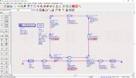
3.2.1 Schematic Circuit Design for Matched Bandstop Filter
The schematic circuit of the matched bandstop filter is designed using the Advanced Design System (ADS) Software. When designing the circuit, it is important to determine all of the important parameters needed to be included into the circuit in order to obtain the desired results. The schematic circuit design consists of:
i. Microstrip Coupled Line (MCLIN) for the gap of the coupled resonator
ii. Microstrip Line (MLIN) iii. Microstrip Bend (Bend)
iv. Terminal (Term) for the input/output port
Figure 3.4: Schematic Circuit Design for Matched Bandstop Filter
3.2.2 Simulation of the Circuit Design
The desired result after simulation of the circuit design are as follows: i. The S11 and S21 response must match at 1GHz ii. The S11 response must be below than -15dB iii. The S21 response must be below than -20dB
23
Figure 3.5: Desired Output Response for the Matched Bandstop Filter After Tuning
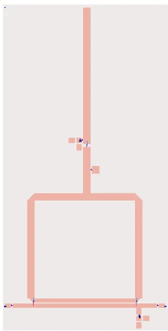
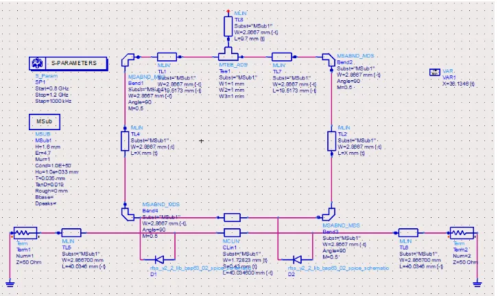
Figure 3.6: Layout Design Figure 3.7: Schematic Design
25 bandpass response. When the voltage supply is turned off for both varactor diodes and PIN diode, a matched bandstop response can be seen and when the voltage supply is turned on for both varactor diodes and PIN diode, the output response shows a bandpass response. The PIN diode at the stub is added in order to give a more precise bandpass response compared to when no PIN diode is added. From the simulation of the layout design and the schematic, it have been proven that the filter now have switchable mode of operations where the switching properties is based on the conditions of the varactor diodes whether it is turned on or turned off to give a bandpass response or a matched bandstop response respectively. The design circuit can then be proceeded for fabrication process.
3.3 FABRICATION
After the circuit design of the switchable matched bandstop to bandpass filter have been successfully produced and the desirable simulation results have been achieved, the fabrication process may take place. The microstrip circuit design is fabricated onto an FR-4 Board with a standard specification as described in Table 3.1 below.
Dielectric Constant, εr Substrate Thickness, H Metal Thickness, T Loss Tangent, D
4.7 1.6mm 0.035mm 0.019
Table 3.1: Substrate’s Specification
difference between the measured results and simulation results may be caused by the etching process where the copper on the FR-4 board is not properly etched, difference in material dielectric across the FR-4 board, active components which varies the readings of the measurement, inaccurate soldering where the components may not be fully connected to the copper and also lossy substrate since the FR-4 board is a low cost substrate.
3.4 PROJECT PLANNING
This part shows the planning of the project implementation and the duration needed for each processes that have to be carried out until the completion of this project as discussed in the methodology section but in the form of flow chart and Gantt chart.
3.4.1 Gantt Chart
27
3.4.2 Flow Chart
29
CHAPTER 4
RESULTS AND DISCUSSION
This chapter discusses on the results that have been obtained during the simulation process of the switchable matched bandstop to bandpass filter design and also the measured results after fabrication had been taken place. Firstly the design and simulation results from both the schematic circuit design and layout design are shown and analyzed. The fabricated product are also shown in this chapter in order to show the size of the filter. Moreover, the measured results after fabricating the filter design are also analyzed. Lastly, both of the results from the simulation and measurement are compared to see whether it shows good agreement between them. The challenges and complications that had been overcome during the process of obtaining the results are stated.
4.1 DESIGN AND SIMULATION RESULTS
The first schematic circuit design of the switchable matched bandstop to bandpass filter shows the components and elements that are required in order to design this filter. These components includes MLIN, MCLIN, MSABND, MTEE, TERM and varactor diode. Since the center frequency is at 1GHz, the start and stop frequency that was set at the S-parameters is 0.8GHz and 1.2GHz respectively. The MTEE represent the stub of the filter and the MCLIN represents the coupling gap of the filter that can be tuned in order to achieve the filter’s specification. The schematic circuit design of the filter is as shown in Figure 4.1 below.
Figure 4.1: First Schematic Circuit Design for the Matched Bandstop to Bandpass Filter
31
Figure 4.2: Matched Bandstop Response from Simulation of the Schematic Circuit Design
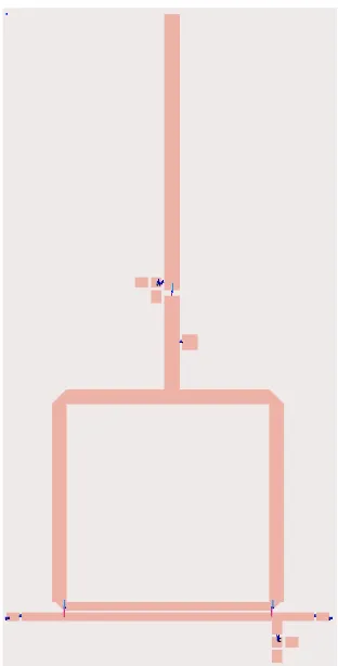
4.1.2 Layout Design and Second Schematic Design
Figure 4.3 shows the layout design of the switchable bandstop to bandpass filter which was converted from the first schematic diagram. The layout is again tuned in order to obtain the best simulation result since the result may differ from the first schematic diagram. In order to see the bandpass response, the second schematic design is produced as shown in Figure 4.4. When the layout is tuned and updated, the second schematic design is also automatically updated. This schematic design provides the response for both matched bandstop and bandpass filter by simply turning on or turning off the vltage supply in the circuit. The matched bandstop and bandpass response obtained after tuning the layout and second schematic design can be seen in Figure 4.5 and Figure 4.6.
33
4.2 FABRICATION OF THE FILTER DESIGN
Figure 4.7: Fabricated Switchable Matched Bandstop to Bandpass Filter
35 simulation which may be due to some factors during the fabrication process. The difference between the measured results and simulation results may be caused by the etching process where the copper on the FR-4 board is not properly etched, difference in material dielectric across the FR-4 board, active components which varies the readings of the measurement, inaccurate soldering where the components may not be fully connected to the copper and also lossy substrate since the FR-4 board is a low cost substrate. The fabricated switchable matched bandstop to bandpass filter is as shown in Figure 4.7.
4.3 MEASURED RESULTS
The fabricated filter is measured by using the Network Analyzer. Before starting the measurement of the filter, student must first calibrate the equipment to be used during the measurement process. Once all of the equipment have been calibrated, the filter ports are connected to port 1 and port 2 of the network analyzer. The DC supply is connected to each resistor at the stub and also at the bottom right of the filter. This is to control the on and off of the varactor diodes and the PIN diode.
4.3.1 Matched Bandstop Response
Figure 4.8: Measured Matched Bandstop Response using Network Analyzer
4.3.2 Bandpass Response
When the DC supply is turned on, the varactor diodes and the PIN diode is in the ON state and therefore produces a bandpass response as shown in Figure 4.8.
37
Figure 4.9: Measured Bandpass Response using Network Analyzer
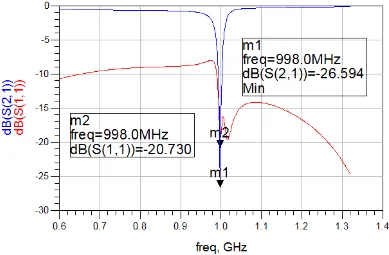
4.4 COMPARISON BETWEEN SIMULATION RESULTS AND MEASURED RESULTS
Parameter Matched Bandstop Filter based on Ring Resonator (size = 7cm x 13cm)
Simulation Measurement
Bandstop Response
(S11), dB -20.730 (< -15) -15.420 (< -15) Bandstop Response
(S21), dB -26.594 (< -20) -35.214 (< -20) Bandpass Response
(S11), (S21)
Q factor 35.643 (> 30) 27.083
39
CHAPTER 5
CONCLUSION AND SUGGESTIONS
5.1 CONCLUSION
5.2IMPORTANCE OF PROJECT DESIGN
There are a lot of importance of designing the switchable matched bandstop to bandpass filter are. Firstly, is having to design a compact filter having two modes of operations in only one filter design. This means that instead of having a number of filter banks, the switchable matched bandstop to bandpass filter reduces the complexity of a system by allowing the filter’s re-configurability to switch from being a bandstop filter to a bandpass filter. Secondly is designing a low cost filter that offers a high performance to the system. This filter uses FR-4 as its substrate which is actually a low cost substrate. However, it offers a high quality factor and gives similar result to that using an expensive substrate. Other than that, this switchable matched bandstop to bandpass filter have better performances compared to a conventional bandstop filter. Compared to a conventional bandstop filter, the switchable matched bandstop to bandpass filter provides a matched bandstop response with a much narrower bandwidth which results to a high Q factor, has no reflected signal and is much more selective. A conventional bandstop filter is quite lossy, has reflected signals in its response which means that it does not fully attenuate the signal and also has a wider bandwidth which results in low quality factor.
5.3 POTENTIAL OF COMMERCIALIZATION
41 5.4 SUGGESTIONS FOR FUTURE WORK
At the end of this project, it can be concluded that the project of designing and developing a matched bandstop to bandpass filter which is based on a dual-mode ring resonator is a success as all of the objectives, specifications and requirements in designing this filter were achieved. However, future work can be done in order to improve the filter’s design to give a much better performance to the system. The future work includes:
1. Repeat the fabrication of the existing design with correct and proper fabrication steps which includes the etching and soldering process and repeat the measurement for the Q factor.
2. Further tuning of the length of the stub and the gap of the MCLIN in order to obtain narrower and lower value of the S11 and S21 response to provide a perfect signal attenuation, no loss and no reflected signal.
3. Use the same concept and method of this filter design to come up with another design of the switchable matched bandstop to bandpass filter that operates at a different operating frequency.
REFERENCES
[1] Andrew C. Guyette, Ian C. Hunter, Roger D. Pollard and Douglas R. Jachowski, “Perfectly-Matched Bandstop Filters using Lossy Resonators”, Naval Research
Laboratory, Washington DC, June.2005.
[2] B. H. Ahmad, M. K. Zahari and P. W. Wong, “Design and Comparison of Reconfigurable Perfectly-Matched Bandstop Filters”, International Journal of Electronics and Computer Science Engineering.
[3] David M. Pozar, “Microwave Engineering, 4th Edition”, John Wiley & Sons Inc, 2012.
[4] Juseop Lee, Eric J. Naglich, Hjalti H. Sigmarsson, Dimitrios Peroulis, Willian J. Chappell, “New Bandstop Filter Circuit Topology and Its Application to Design of a Bandstop-to-Bandpass Switchable Filter”, IEEE Transactions on Microwave
Theory and Techniques, Vol. 61, March.2013.
[5] A. A. Bakhit and W. P. Wong, “Switchable Band-stop to All Pass Filter Using Stepped Impedance Resonator”, PIERS Proceedings, Stockholm, Sweden, Aug. 12-15.2013.
[6] A. A. Bakhit, W. P. Wong and M. S. Osman, “Switchable Matched Band-stop Filter for High Power Interference Mitigation”, Asia-Pacific Microwave
43
[7] Sacid Oruc, “Electronically Tunable Microwave Bandstop Filter Design and Implementation”, The Graduate School of Natural and Applied Sciences of Middle
East Technical University, Sep.2010.
[8] F.C. Chen, N. Y. Zhang, Q. X. Chu, “Design of Ultrawideband Banstop Filter Using Defected Ground Structure”, IET Electron. Lett.,Aug.2013.
[9] Skyworks Solution Inc, “Design with PIN Diodes”, Skyworks Application Notes, Oct.2012.
[10] Sha Luo, Lei Zhu, Sheng Sun, “New Studies on Microstrip Ring Resonators for Compact Dual-Mode Dual- and Triple-Band Bandpass Filter”, Department of
Electrical and Electronic Enginnering, University of Hong Kong, China, 2014.
[11] M. Matsuo, H. Yabuki, M. Makimoto, “Dual-Mode Stepped-Impedance Ring Resonator for Bandpass Filter Applications”, IEEE Transactions on Microwave
Theory and Techniques, July.2001.
[12] Eric J. Naglich, Juseop Lee, Dimitrios Peroulis, William J. Chappell, “Switchless Tunable Bandstop-to-All-Pass Reconfigurable Filter”, IEEE Transactions on
Microwave Theory and Techniques, May.2012.
[13] I. Hunter, R. Ranson, A. Guyette, A. Abunjaileh, “Microwave Filter Design form a Systems Perspective”, IEEE Microwave Magazine, Oct.2007.
[14] P. Rani, S. Gupta, R. K. Prasad, “Design & Optimization of Microstrip Parallel Coupled Bandpass Filter at 20GHz”, International Journal of Advanced Research
in Computer Engineering & Technology (INJARCET), May.2014.
[15] M. Moradian, M. Khalaj-Amirhosseini, “Improvement of the Characteristics of the Microstrip Parallel Coupled Line Coupler by Means of Grooved Substrate”,
[16] S. Seghier, N. Benahmed, F. T. Bendimerad, “Design of Parallel Coupled Microstrip Bandpass Filter for FM Wireless Applications”, 6th International
Conference on Sciences of Electronics, Technologies of Information and
Telecommunications (SETIT), 2012.
[17] J. Marimuthu, M. Esa, “Harmonic Cancellation of Parallel-Coupled Bandpass Filter with Transmission Zero Realign Method”, Asia-Pacific Conference on
Applied Electromagnetics Proceedings, Dec.2005.
[18] Y. H. Cho, Gabriel M. Rebeiz, “Two and Four-Pole Tunable 0.7-1.1-GHz Bandpass-to-Bandstop Filters with Bandwidth Control”, IEEE Transactions on
Microwave Theory and Techniques, 2014.
[19] C. H. Tseng, T. Itoh, “Dual-Band Bandpass and Bandstop Filters Using Composite Right/Left-Handed Matematerial Transmission Lines”, 2006 IEEE MTT-S
International Microwave Symposium Digest, 2006.
[20] A. Batmanov, E. Burte, R. Mikuta, A. Boutejdar, A. Omar, A. Khaidurova, “Design of Coplanar Bandstop Filter Based on Open-loop-ring Resonator and DGS for WLAN and UWB Applications”, Microwave Integrated Circuits
Conference (EuMIC), 2012 7th Europian, 2012.