UNIVERSITI TEKNIKAL MALAYSIA, MELAKA
DESIGN AND ANALYSIS OF MODULAR FIXTURE OF PCB
ROUTING MACHINE
This report submitted in accordance of with the requirement of the Universiti Teknikal Malaysia Melaka (UTeM) for the Bachelor Degree of Manufacturing
Engineering (Manufacturing Design) with Honours.
by
MOHD FARID BIN GHAZALI
UTeM Library (Pind.1/2007)
UNIVERSITI TEKNIKAL MALAYSIA MELAKA
BORANG PENGESAHAN STATUS TESIS*
JUDUL:Design and Analysis of Modular Fixture of PCB Routing Machine
SESI PENGAJIAN: 2009-20010
Saya _____________________________________________________________________
mengaku membenarkan tesis (PSM/Sarjana/Doktor Falsafah) ini disimpan di Perpustakaan Universiti Teknikal Malaysia Melaka (UTeM) dengan syarat-syarat kegunaan seperti berikut:
1. Tesis adalah hak milik Universiti Teknikal Malaysia Melaka.
2. Perpustakaan Universiti Teknikal Malaysia Melaka dibenarkan membuat salinan
untuk tujuan pengajian sahaja.
3. Perpustakaan dibenarkan membuat salinan tesis ini sebagai bahan pertukaran
DECLARATION
I hereby, declared this report entitled “Design and Analysis of Modular Fixture of PCB Routing Machine” is the results of my own research except as cited in
references.
Signature : ………...
Author’s Name : ……….
APPROVAL
This report is submitted to the Faculty of Manufacturing Engineering of UTeM as a partial fulfillment of the requirements for the degree of Bachelor of Manufacturing Engineering (Manufacturing Design). The member of the supervisory committee is as follow:
……… (Mr. Ismail Bin Abu Shah)
ABSTRACT
ABSTRAK
DEDICATION
ACKNOWLEDGEMENT
TABLE OF CONTENT
2.1 Background of Printed Circuit Board (PCB) 8
2.1.1 PCB History 10
2.1.2 PCB Warpage 11
2.2 Workholding - Jigs and Fixtures 12
2.2.1 Principles of Workholding 13
2.2.1.1 Locating 13
2.2.1.2 Clamping 16
2.3 Fixtures 18
2.3.1 Fixture Configurations 19
2.3.2 Fixture Design Process 20
2.4 Modular Fixture 21
2.4.1 Modular Fixture System 23
2.4.1.2 Dowel-Pin-Based Modular Fixtures 24 2.4.1.3 Comparison between T-slot based and Dowel-pin based 26
2.5 PCB Routing 28
2.5.1 Pin Routing 28
2.5.2 CNC Routing Applications 29
2.5.3 CNC Operations 30
2.5.4 Mechanical Routing with CNC Equipment 31
2.5.5 Summarizing of PCB Routing 34
2.6 PCB Depanelize 35
2.6.1 PCB Strain Analysis 36
2.6.2 BGA Assembly Strain Measurement 39
3.0 METHODOLOGY 41
3.1 Introduction 41
3.2 Project Planning 41
3.2.1 Statement of Work (Gantt chart) 42
3.3 Project Flow 44
3.3.1 Identify Problem and Defining of Project Objectives and Scope 45 3.3.2 Literature Review and Existing Method 45
3.3.3 PCB Modular Fixture Design 46
3.3.4 Experimental Analysis, Simulation and Verification 46
4.4.2 Fixture Components 56
4.5 PCB Cutting Preparation 63
4.5.1 PCB Loading and Unloading 64
4.5.2 Holding and Gripping Process 65
4.5.3 Strain Gauge Connection 66
4.6 PCB Cutting Analysis 67
4.6.1 Strain Gauge Point 68
4.6.2 Locating Pin and Supporter Position 68
4.6.3 PCB Cutting Parameter 72
4.6.4 The Output 74
4.6.5 Strain Analysis 75
4.7 Final Position and Location 82
5.0 DISCUSSION 83
5.1 Fixture Design 83
5.1.1 The Reason for Using Dowel Pin Base Modular Fixture 83 5.1.2 Assembly of Sliding Base, Supporter, Locating Pin, and Vacuum Pad 84
5.1.3 Suction System 85
5.4.3 Strain Gauge Connection 89
5.4.4 Cutting Parameters and Cutting Direction 91
5.4.5 The PCB Figure after Cutting 92
6.0 CONCLUSION AND RECOMMENDATION 97
6.1 Conclusion 97
6.2 Research Barriers 99
6.3 Recommendations 99
REFERENCES 102
LIST OF TABLES
2.1 Comparison of T-slot and Dowel-pin modular fixtures 27
2.2 Various depaneling methods 35
3.1 Project Gantt chart for PSM 1 40
3.2 Project Gantt chart for PSM II 41
4.1 Locating pin and supporter used for 3 difference conditions 70
4.2 Cutting parameters 71
4.3 Strain gauge results 79
CHAPTER 1
INTRODUCTION
This report described a project on the design and analysis of modular fixture for Printed Circuit Board (PCB) routing machine. In this research, the modular fixture becomes a work holding device for PCB cutting operation by using the routing machine.
1.1 Background
The work holding device can be defined as a device used to locate and hold a workpiece. The work holding device references the tool performing the operation on the part being held. Basically, the work holding device is widely used in manufacturing industries, where, most of manufacturing processes include machining, assembly, joining, and also inspection of part required the use of work holding device.
Technically, the work holding device can be divided into four categories; standard devices, jigs, fixtures, and modular fixturing system. Each type has it own capability to hold the part in certain conditions. Furthermore, it can be designed either in automated or manually operated.
A printed circuit board, or PCB, is a self-contained module of interconnected electronic components found in devices ranging from common beepers, or pagers, and radios to sophisticated radar and computer systems. The circuits are formed by a thin layer of conducting material deposited, or "printed," on the surface of an insulating board known as the substrate. Individual electronic components are placed on the surface of the substrate and soldered to the interconnecting circuits. Contact fingers along one or more edges of the substrate act as connectors to other PCBs or to external electrical devices such as on-off switches. A printed circuit board may have circuits that perform a single function, such as a signal amplifier, or multiple functions.
Depaneling is a process step in high-volume electronics assembly operation. In order to increase the throughput of PCB manufacturing and surface mount technology lines, PCBs are often designed so that they consist of many smaller individual PCBs that will be used in the final product. This PCB cluster is called a panel or multiblock. The large panel is broken up or “depaneled” as a certain step in the process depending on the product, it may happen right after SMT process, after in-circuit test (ICT), after soldering of through-hole elements, or even right before the final case up of the assembly.
Furthermore, the depaneling process is relatively similar as the PCB cutting in industry. Basically, the cutting operation is done manually or automatically based on the accuracy needed for the final product of the PCB. In term of accuracy and the ability of the cutting operation, the automatic approach is usually used together with the other elements that include fixture and holding elements. Besides that, the movement of cutting is controlled by robot movement that will cut the PCBs according to the robot program. Moreover, this cutting operation is also known as the PCB routing operation.
routing process is succeed without damaging the components and the board itself, a proper fixture should be used together to hold the PCB during the cutting of PCB. The fixture is not only to hold the PCB, but also to maintain the accuracy of cutting and to prevent any abnormalities to the board including crack propagation and warping.
1.2 Problem Statement
PCB cutting or depaneling is not an easy process. In modern manufacturing environment where surface-mount components are the norm, depaneling methods such as V-scores and various hand-break methods may be risky. Reliably and repeatably controlling the forces required to depanel the PCB is difficult. If a ceramic capacitor is damaged, for example, the defect may then show up as a field failure. These kinds of defects can slip right through a functional test.
One significant problem related to the PCB cutting is crack or warping cause by high force given during the operation. Normally, in manual cutting operation which is usually using the hand to break the PCB, the force given is not constant due to the energy of human being. Since the force is not consistent, the PCB is highly risk to be damaged in term of warping or crack. It will lead to failure for the PCB to be functioned. Furthermore, there is no specific equipment used to analyze and measure the PCB if any abnormality happened. By using the naked eye, it is not impossible to find out which part of the PCB got crack or warping, but if the amount of crack is too little, it might be difficult to the user to determine the infected area.
and the tool bit used are the other things to consider as the cutting strategy by using the automatic cutting methods.
Another problem associated with the PCB cutting is that the holding method used during the PCB cutting operation. By mean of that, the jigs or fixtures used for holding the PCB are not good enough to prevent the PCB from warping or damage. Basically, the problem is happened due to the unsuitable jigs or fixtures used. The jigs or fixtures should not be used only for holding the PCB. It is required for the jigs or fixtures to absorb the force, stress and strain during the cutting operation. Moreover, most of the jigs or fixtures used are not modular, that is much better to hold and locate the PCB well. In addition, the locating of PCB onto the fixture is not proper enough. Technically, it will lead to the unstable condition to the PCB for the cutting operation. The vibration from the cutting operation will damage the PCB and makes the PCB fail to function.
1.3 Objective of Study
There are two main objectives from this research. There are as follows:
a. To design a PCB modular fixture to hold and locate the PCB during the cutting operation for cutting stability.
b. To analyze the optimum holding and locating method for PCB cutting by using strain gauge.
1.4 Scope of Study
This study will cover the design and analysis of PCB fixture for PCB cutting operation. The fixture will be a modular fixture used to cut the PCB by using the routing machine. The experimental analysis will be conducted to find out the most optimum holding and locating condition for the PCB during the cutting operation. The PCB fixture will design according to the routing machine standard by using computer software, while the experimental analysis will use the strain gauge to measure the vibration, crack propagation, and warping during the PCB cutting operation. The most optimum holding and locating condition will be identified then.
1.5 Project Outline
project, and also the project outline which is briefly explain the subtopics related to this project.
b. Chapter 2 - Literature Review
This chapter is all about the knowledge and information of the project. Basically, it is the theoretical knowledge regarding to the project title which is help in understanding the project as well.
c. Chapter 3 – Methodology
This chapter is focusing on the flow of the project from the beginning until the project done. Besides that, it also shows the general explanation of each process of methodology involves in this project. Others, the tools and analysis techniques use for designing and analyzing the PCB fixture are also stated.
d. Chapter 4 – Result and Analysis
This chapter will show the result of the PCB fixture design for the cutting operation. Other than that, the method of conducting the experimental analysis also shows in this chapter. Furthermore, the analysis result from the PCB cutting operation also included.
e. Chapter 5 – Discussion
This chapter will describe in detail the results of this project. It will focus on the explanation of PCB fixture, the routing machine used to cut the PCB, and the process involved for the PCB cutting operation. Others, the most optimum holding and locating condition for PCB also stated in this chapter.
f. Chapter 6 – Conclusion
CHAPTER 2
LITERATURE REVIEW
2.1 Background of Printed Circuit Board (PCB)
A printed circuit board, or PCB, is a self-contained module of interconnected electronic components found in devices ranging from common beepers, or pagers, and radios to sophisticated radar and computer systems. The circuits are formed by a thin layer of conducting material deposited, or "printed," on the surface of an insulating board known as the substrate. Individual electronic components are placed on the surface of the substrate and soldered to the interconnecting circuits. Contact fingers along one or more edges of the substrate act as connectors to other PCBs or to external electrical devices such as on-off switches. A printed circuit board may have circuits that perform a single function, such as a signal amplifier, or multiple functions. (Carvette C., 2000).
Components on a printed circuit board are electrically connected to the circuits by two different methods: the older "through hole technology" and the newer "surface mount technology." (Ford D.N., 2001). With through hole technology, each component has thin wires, or leads, which are pushed through small holes in the substrate and soldered to connection pads in the circuits on the opposite side. Gravity and friction between the leads and the sides of the holes keeps the components in place until they are soldered. With surface mount technology, stubby J-shaped or L-shaped legs on each component contact the printed circuits directly. A solder paste consisting of glue, flux, and solder are applied at the point of contact to hold the components in place until the solder is melted, or "reflowed," in an oven to make the final connection. Although surface mount technology requires greater care in the placement of the components, it eliminates the time-consuming drilling process and the space-consuming connection pads inherent with through hole technology.
Two other types of circuit assemblies are related to the printed circuit board. An integrated circuit, sometimes called an IC or microchip, performs similar functions to a printed circuit board except the IC contains many more circuits and components that are electrochemically "grown" in place on the surface of a very small chip of silicon. A hybrid circuit, as the name implies, looks like a printed circuit board, but contains some components that are grown onto the surface of the substrate rather than being placed on the surface and soldered.
2.1.1 PCB History
Printed circuit boards evolved from electrical connection systems that were developed in the 1850s. Metal strips or rods were originally used to connect large electric components mounted on wooden bases. In time the metal strips were replaced by wires connected to screw terminals, and wooden bases were replaced by metal chassis. But smaller and more compact designs were needed due to the increased operating needs of the products that used circuit boards. In 1925, Charles Ducas of the United States submitted a patent application for a method of creating an electrical path directly on an insulated surface by printing through a stencil with electrically conductive inks. This method gave birth to the name "printed wiring" or "printed circuit." (Carvette C., 2000).
In the 1943, Paul Eisler of the United Kingdom patented a method of etching the conductive pattern, or circuits, on a layer of copper foil bonded to a glass-reinforced, non-conductive base. Widespread use of Eisler's technique did not come until the 1950s when the transistor was introduced for commercial use. Up to that point, the size of vacuum tubes and other components were so large that the traditional mounting and wiring methods were all that was needed. With the advent of transistors, however, the components became very small, and manufacturers turned to printed circuit boards to reduce the overall size of the electronic package. (Ford D.N., 2001).
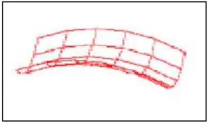
2.1.2 PCB Warpage
Warpage is the out of plane deformation of the artefact (which is PCB in this research), caused by differential (non-homogenous) shrinkage or expansion of elements composing the artifact. (Klein et al., 2004). In this research, it will focus on thermally induced warpage, i.e. warpage of the PCB when it is subjected to the thermal loading. Increasingly, local warpage, e.g. warpage in the region of critical component footprint, is a more critical issue than global warpage, the warpage of the PCB as a hole. Changes in the contour of the component footprint can create shorts or opens in the PCB component solder joints during cutting operation or build stresses into the assembly that appear as later reliability problem (Klein et al., 2004).
Figure 2.2: Out of plane deformation of a linear element (Klein, 2004)