LM35
Product Folder
1 Features
LM35 Precision Centigrade Temperature Sensors
• Calibrated Directly in Celsius (Centigrade)
• Linear + 10-mV/°C Scale Factor
• 0.5°C Ensured Accuracy (at 25°C)
• Rated for Full −55°C to 150°C Range
• Suitable for Remote Applications
• Low-Cost Due to Wafer-Level Trimming
• Operates from 4 V to 30 V
• Less than 60-
μ
A Current Drain
• Low Self-Heating, 0.08°C in Still Air
• Non-Linearity Only ±¼°C Typical
• Low-Impedance Output, 0.1
Ω
for 1
2 Applications
• Power Supplies
• Battery Management
• HVAC
• Appliances
Basic Centigrade Temperature Sensor
+V
S(2°C to 150°C)
(4 V to 20 V)
OUTPUT
LM35
Sample &
Buy Technical Documents Tools & Software Support & Community
SNIS159G – AUGUST 1999
LM35 Precision Centigrade Temperature Sensors
3 Description
(Centigrade)
25°C)
Range
Trimming
Air
for 1-mA Load
Basic Centigrade Temperature Sensor
The LM35 series are precision integrated
temperature devices with an output voltage linearly
proportional to the Centigrade temperature. The
LM35 device has an advantage over linear
temperature sensors calibrated in Kelvin, as the user
is not required to subtract a large constant voltage
from the output to obtain convenient Centigrade
scaling. The LM35 device does not require any
external calibration or trimming to provide typical
accuracies of ±¼°C at room temperature and ±¾°C
over a full −55°C to 150°C temperature range. Lower
cost is assured by trimming
wafer level. The low-output impedance, linear output,
and precise inherent calibration of the LM35 device
makes interfacing to readout or control circuitry
especially easy. The device is used with single power
supplies, or with plus and minus supplies. As the
LM35 device draws only 60
very low self-heating of less than 0.1°C in still air. The
LM35 device is rated to operate over a
150°C temperature range, while the LM35C device is
rated for a −40°C to 110°C range (
improved accuracy). The LM35
available packaged in hermetic TO transistor
packages, while the LM35C, LM35CA, and LM35D
devices are available in the plastic TO
package. The LM35D device is availabl
surface-mount small-outline package and a plastic
TO-220 package.
Device Information
PART NUMBER PACKAGE
LM35
TO-CAN (3) TO-92 (3) SOIC (8) TO-220 (3)
(1) For all available packages, see the orderable addendum at the end of the datasheet.
Full-Range Centigrade Temperature
+V
SLM35
Support & CommunityLM35
AUGUST 1999 – REVISED AUGUST 2016
LM35 Precision Centigrade Temperature Sensors
The LM35 series are precision integrated-circuit
devices with an output voltage linearly-
proportional to the Centigrade temperature. The
LM35 device has an advantage over linear
temperature sensors calibrated in Kelvin, as the user
is not required to subtract a large constant voltage
obtain convenient Centigrade
scaling. The LM35 device does not require any
external calibration or trimming to provide typical
accuracies of ±¼°C at room temperature and ±¾°C
−55°C to 150°C temperature range. Lower
cost is assured by trimming and calibration at the
output impedance, linear output,
and precise inherent calibration of the LM35 device
makes interfacing to readout or control circuitry
especially easy. The device is used with single power
and minus supplies. As the
LM35 device draws only 60
μ
A from the supply, it has
heating of less than 0.1°C in still air. The
LM35 device is rated to operate over a −55°C to
150°C temperature range, while the LM35C device is
to 110°C range (−10° with
improved accuracy). The LM35-series devices are
available packaged in hermetic TO transistor
packages, while the LM35C, LM35CA, and LM35D
devices are available in the plastic TO-92 transistor
package. The LM35D device is available in an 8-lead
outline package and a plastic
Device Information
(1)PACKAGE BODY SIZE (NOM) CAN (3) 4.699 mm × 4.699 mm 92 (3) 4.30 mm × 4.30 mm SOIC (8) 4.90 mm × 3.91 mm
220 (3) 14.986 mm × 10.16 mm (1) For all available packages, see the orderable addendum at
Range Centigrade Temperature Sensor
LM35
SNIS159G – AUGUST 1999 – REVISED AUGUST 2016
1 Features
...
2 Applications
...
3 Description
...
4 Revision History
...
5 Pin Configuration and Functions
6 Specifications
...
Absolute Maximum Ratings ... ESD Ratings ... Recommended Operating Conditions... Thermal Information ... Electrical Characteristics: LM35A, LM35CA Limits... Electrical Characteristics: LM35A, LM35CA
Electrical Characteristics: LM35, LM35C, LM35D Limits Electrical Characteristics: LM35, LM35C, LM35D ... 6.9 Typical Characteristics ...
7 Detailed Description
...
Overview ... Functional Block Diagram ...
4 Revision History
Changes from Revision F (January 2016) to
•
Equation 1
, changed From: 10 mV/°F
•
Power Supply Recommendations
, changed From: "4
Changes from Revision E (January 2015) to
• Changed NDV Package (TO-CAN) pinout from Top View to
Changes from Revision D (October 2013) to
• Added
Pin Configuration and Functions
Modes
,
Application and Implementation
and Documentation Support
section, and
Changes from Revision C (July 2013) to
• Changed
W
to
Ω
...
• Changed
W
to
Ω
in
Abs Max
tablenote.
AUGUST 2016Table of Contents
...
1
...
1
...
1
...
2
Functions
...
3
...
4
... 4
... 4
... 4
... 4
Electrical Characteristics: LM35A, LM35CA Limits... 5
LM35CA ... 6
Electrical Characteristics: LM35, LM35C, LM35D Limits ... 8
Electrical Characteristics: LM35, LM35C, LM35D ... 9
... 11
...
13
... 13
... 13
Feature Description Device Functional Modes
8 Application and Implementation
Application Information Typical Application System Examples9 Power Supply Recommendations
10 Layout
...
Layout Guidelines Layout Example ...11 Device and Documentation Support
Receiving Notification of Documentation Updates 11.2 Community Resources Trademarks... Electrostatic Discharge Caution Glossary 2112
Mechanical, Packaging, and Orderable
Information
...
Changes from Revision F (January 2016) to Revision G
, changed From: 10 mV/°F To: 10mv/°C
...
, changed From: "4-V to 5.5-V power supply" To: "4-V to 30
Changes from Revision E (January 2015) to Revision F
CAN) pinout from Top View to Bottom View
...
Changes from Revision D (October 2013) to Revision E
Pin Configuration and Functions
section,
ESD Ratings
table,
Feature Description
section,
Application and Implementation
section,
Power Supply Recommendations
section,
section, and
Mechanical, Packaging, and Orderable Information
Changes from Revision C (July 2013) to Revision D
...
tablenote.
...
www.ti.com Feature Description ...13Device Functional Modes ... 13
Implementation
...
14
Information ... 14
Application ... 15
Examples ... 16
Power Supply Recommendations
...
19
...
19
Guidelines ... 19
... 20
Documentation Support
...
21
Receiving Notification of Documentation Updates 21 Resources ... 21
... 21
Caution ... 21
Mechanical, Packaging, and Orderable
...
21
Page
... 13
V to 30-V power supply:
... 19
Page
... 3
Page
section,
Device Functional
section,
Layout
section,
Device
Information
section
... 1
Page
...
1
www.ti.com
5 Pin Configuration and Functions
NDV Package 3-Pin TO-CAN (Bottom View)
Case is connected to negative pin (GND)
D Package 8-PIN SOIC (Top View)
V
OUTN.C.
N.C.
GND
N.C. = No connection
LP Package 3-Pin TO-92 (Bottom View)
PIN
NAME TO46 TO92 TO220
VOUT — —
N.C. — —
— —
GND — —
N.C.
— —
— —
— —
+VS — —
+V
SV
OUTGND
+V
SV
OUTGND
−1
2
3
4
8
7
6
5
SNIS159G – AUGUST
Functions
Case is connected to negative pin (GND)
NEB Package 3-Pin TO
(Top View)
+V
SN.C.
N.C.
+V
SGND
N.C.
Tab is connected to the negative pin(GND).
NOTE: The LM35DT pinout is different than the discontinued LM35DP
Pin Functions
TYPE
TO220 SO8
— 1 O Temperature Sensor Analog Output
— 2
— No Connection
— 3
— 4 GROUND Device ground pin, connect to power terminal
— 5
— No Connection
— 6
— 7
— 8 POWER Positive power supply pin
GND
LM
35DT
LM35
AUGUST 1999 – REVISED AUGUST 2016
NEB Package Pin TO-220 (Top View)
GND
V
OUTTab is connected to the negative pin
The LM35DT pinout is different than the discontinued LM35DP
DESCRIPTION
Temperature Sensor Analog Output
Device ground pin, connect to power supply negative
Positive power supply pin
LM
35DT
LM35
SNIS159G – AUGUST 1999 – REVISED AUGUST 2016
6 Specifications
Absolute Maximum Ratings
over operating free-air temperature range (unless otherwise noted)
Supply voltage Output voltage Output current
Maximum Junction Temperature, TJmax
Storage Temperature, Tstg
TO-(1) If Military/Aerospace specified devices are required, please contact the Texas Instruments Sales Office/ Distributors for availability and specifications.
(2) Absolute Maximum Ratings indicate limits beyond which damage to the device may occur. DC and AC electrical specifications do apply when operating the device beyond its rated operating
ESD Ratings
V(ESD) Electrostatic discharge Human (1) JEDEC document JEP155 states that
Recommended Operating Conditions
over operating free-air temperature range (unless otherwise noted)
Specified operating temperature: TMIN to TMAX
Supply Voltage (+VS)
Thermal Information
THERMAL METRIC(1)(2)
RθJA Junction-to-ambient thermal resistance RθJC(top) Junction-to-case (top) thermal resistance
(1) For more information about traditional and new thermal metrics, see the (2) For additional thermal resistance information, see
AUGUST 2016
air temperature range (unless otherwise noted)
(1)(2)-CAN, TO-92 Package -220, SOIC Package
devices are required, please contact the Texas Instruments Sales Office/ Distributors for availability and Absolute Maximum Ratings indicate limits beyond which damage to the device may occur. DC and AC electrical specifications do
y when operating the device beyond its rated operating conditions.
Human-body model (HBM), per ANSI/ESDA/JEDEC JS-001(1)
-V HBM allows safe manufacturing with a standard ESD control process.
Conditions
air temperature range (unless otherwise noted)
MIN
LM35, LM35A –
LM35C, LM35CA –
LM35D
LM35
NDV LP
3 PINS 8 PINS
resistance 400 180
case (top) thermal resistance 24 —
For more information about traditional and new thermal metrics, see the IC Package Thermal Metrics
For additional thermal resistance information, see Typical Application.
www.ti.com
MIN MAX UNIT
–0.2 35 V
–1 6 V
10 mA
150 °C
–60 150
°C
–65 150
devices are required, please contact the Texas Instruments Sales Office/ Distributors for availability and Absolute Maximum Ratings indicate limits beyond which damage to the device may occur. DC and AC electrical specifications do not
VALUE UNIT
±2500 V
manufacturing with a standard ESD control process.
MIN MAX UNIT
–55 150
°C
–40 110
0 100
4 30 V
UNIT
D NEB
8 PINS 3 PINS
220 90
°C/W
— —
www.ti.com
Electrical Characteristics: LM35A, LM35CA
Unless otherwise noted, these specifications apply:
LM35C and LM35CA; and 0°C ≤ T
J≤ 100°C for the LM35D. V
Centigrade Temperature Sensor
. These specifications also apply from 2°C to T
PARAMETER TEST CONDITIONS
Accuracy (3)
TA = 25°C TA = –10°C TA = TMAX TA = TMIN
Nonlinearity(4) TMIN ≤ TA ≤ TMAX, –40°C ≤ TJ ≤ 125°C Sensor gain
(average slope)
TMIN ≤ TA ≤ TMAX –40°C ≤ TJ ≤ 125°C
Load regulation(5) 0 ≤ IL ≤ 1 mA
TA = 25°C TMIN ≤ TA ≤ TMAX, –40°C ≤ TJ ≤ 125°C
Line regulation(5) TA = 25°C 4 V ≤ VS ≤ 30 V, –40°C ≤ TJ ≤ 125°C
Quiescent current(6)
VS = 5 V, 25°C VS = 5 V, –40°C ≤ TJ VS = 30 V, 25°C VS = 30 V, –40°C ≤ T
Change of quiescent current(5)
4 V ≤ VS ≤ 30 V, 25°C 4 V ≤ VS ≤ 30 V, –40°C ≤ TJ ≤ 125°C Temperature
coefficient of
quiescent current –40°C ≤ TJ ≤ 125°C Minimum temperature
for rate accuracy In circuit of Figure 14 Long term stability TJ = TMAX, for 1000 hours (1) Tested Limits are ensured and 100% tested in (2) Design Limits are ensured (but not 100%
not used to calculate outgoing quality levels.
(3) Accuracy is defined as the error between the output voltage and 10 mv/°C times the case temperature of the device, conditions of voltage, current, and temperature (expressed in
(4) Non-linearity is defined as the deviation of the output temperature range of the device.
(5) Regulation is measured at constant junction temperature, using pulse testing with a low duty cycle. Changes in output due to heatin effects can be computed by multiplying the internal dissipation by the thermal
(6) Quiescent current is defined in the circuit of
SNIS159G – AUGUST
Electrical Characteristics: LM35A, LM35CA Limits
Unless otherwise noted, these specifications apply: −55°C ≤ T
J≤ 150°C for the LM35 and LM35A;
≤ 100°C for the LM35D. V
S= 5 Vdc and I
LOAD= 50
μ
A, in the circuit of
. These specifications also apply from 2°C to T
MAXin the circuit of
TEST CONDITIONS TYP TESTED LM35A DESIGN
LIMIT(1) LIMIT(2) TYP
±0.2 ±0.5 ±0.2
±0.3 ±0.3
±0.4 ±1 ±0.4
±0.4 ±1 ±0.4
±0.18 ±0.35 ±0.15
10 9.9 10
10 10.1 10
±0.4 ±1 ±0.4
±0.5 ±3 ±0.5
±0.01 ±0.05 ±0.01
±0.02 ±0.1 ±0.02
56 67 56
J ≤ 125°C 105 131 91
56.2 68 56.2
≤ TJ ≤ 125°C 105.5 133 91.5
≤ 30 V, 25°C 0.2 1 0.2
0.5 2 0.5
0.39 0.5 0.39
Figure 14, IL = 0 1.5 2 1.5
, for 1000 hours ±0.08 ±0.08
Tested Limits are ensured and 100% tested in production.
Design Limits are ensured (but not 100% production tested) over the indicated temperature and supply voltage ranges. These limits are levels.
Accuracy is defined as the error between the output voltage and 10 mv/°C times the case temperature of the device, conditions of voltage, current, and temperature (expressed in °C).
linearity is defined as the deviation of the output-voltage-versus-temperature curve from the
best-tion is measured at constant juncbest-tion temperature, using pulse testing with a low duty cycle. Changes in output due to heatin effects can be computed by multiplying the internal dissipation by the thermal resistance.
rcuit of Figure 14.
LM35
AUGUST 1999 – REVISED AUGUST 2016
≤ 150°C for the LM35 and LM35A; −40°C ≤ T
J≤ 110°C for the
A, in the circuit of
Full-Range
in the circuit of
Figure 14
.
LM35CA
UNIT TYP TESTED DESIGN
LIMIT(1) LIMIT(2)
±0.2 ±0.5
°C
±0.3 ±1
±0.4 ±1
±0.4 ±1.5
±0.15 ±0.3 °C
10 9.9
mV/°C
10 10.1
±0.4 ±1
mV/mA
±0.5 ±3
±0.01 ±0.05
mV/V
±0.02 ±0.1
56 67
µA
91 114
56.2 68
91.5 116
0.2 1
µA
0.5 2
0.39 0.5 µA/°C
1.5 2 °C
±0.08 °C
production tested) over the indicated temperature and supply voltage ranges. These limits are Accuracy is defined as the error between the output voltage and 10 mv/°C times the case temperature of the device, at specified
LM35
SNIS159G – AUGUST 1999 – REVISED AUGUST 2016
Electrical Characteristics: LM35A,
Unless otherwise noted, these specifications apply:
LM35C and LM35CA; and 0°C ≤ T
J≤ 100°C for the LM35D. V
Centigrade Temperature Sensor
. These specifications also apply from 2°C to T
PARAMETER TEST CONDITIONS
Accuracy (1)
TA = 25°C
TA = –10°C
TA = TMAX
TA = TMIN
Nonlinearity(4) TMIN ≤ TA ≤ TMAX, –40°C ≤ TJ ≤ 125°C
Sensor gain (average slope)
TMIN ≤ TA ≤ TMAX
–40°C ≤ TJ ≤ 125°C
Load regulation(5) 0 ≤ IL ≤ 1 mA
TA = 25°C
TMIN ≤ TA ≤ TMAX, –40°C ≤ TJ ≤ 125°C
Line regulation(5)
TA = 25°C
4 V ≤ VS ≤ 30 V, –40°C ≤ TJ ≤ 125°C
AUGUST 2016
Electrical Characteristics: LM35A, LM35CA
Unless otherwise noted, these specifications apply: −55°C ≤ T
J≤ 150°C for the LM35 and LM35A;
≤ 100°C for the LM35D. V
S= 5 Vdc and I
LOAD= 50
μ
A, in the circuit of
. These specifications also apply from 2°C to T
MAXin the circuit of
TEST CONDITIONS LM35A
MIN TYP MAX ±0.2
Tested Limit(2) ±0.5
Design Limit(3)
±0.3 Tested Limit(2)
Design Limit(3)
±0.4
Tested Limit(2) ±1
Design Limit(3)
±0.4
Tested Limit(2) ±1
Design Limit(3)
±0.18 Tested Limit(2)
Design Limit(3) ±0.35
10
Tested Limit(2) 9.9
Design Limit(3)
10
Tested Limit(2) 10.1
Design Limit(3)
±0.4
Tested Limit(2) ±1
Design Limit(3)
±0.5 Tested Limit(2)
Design Limit(3) ±3
±0.01
Tested Limit(2) ±0.05
Design Limit(3)
±0.02 Tested Limit(2)
Design Limit(3) ±0.1
www.ti.com
≤ 150°C for the LM35 and LM35A; −40°C ≤ T
J≤ 110°C for the
A, in the circuit of
Full-Range
in the circuit of
Figure 14
.
LM35CA UNIT
www.ti.com
Electrical Characteristics: LM35A, LM35CA (continued)
Unless otherwise noted, these specifications apply:
LM35C and LM35CA; and 0°C ≤ T
J≤ 100°C for the LM35D. V
Centigrade Temperature Sensor
. These specifications also apply from 2°C to T
PARAMETER TEST CONDITIONS
Quiescent current(6)
VS = 5 V, 25°C
VS = 5 V,
–40°C ≤ TJ ≤ 125°C
VS = 30 V, 25°C
VS = 30 V, –40°C ≤ TJ ≤ 125°C
Change of quiescent current(5)
4 V ≤ VS ≤ 30 V, 25°C
4 V ≤ VS ≤ 30 V, –40°C ≤ TJ ≤ 125°C
Temperature coefficient of
quiescent current –40°C ≤ TJ ≤ 125°C
Minimum temperature for rate accuracy
In circuit of Figure 14, IL = 0
Long term
stability TJ = TMAX, for 1000 hours (6) Quiescent current is defined in the circuit of
SNIS159G – AUGUST
lectrical Characteristics: LM35A, LM35CA (continued)
Unless otherwise noted, these specifications apply: −55°C ≤ T
J≤ 150°C for the LM35 and LM35A;
≤ 100°C for the LM35D. V
S= 5 Vdc and I
LOAD= 50
μ
A, in the circuit of
. These specifications also apply from 2°C to T
MAXin the circuit of
TEST CONDITIONS MIN LM35A TYP MAX56
Tested Limit(2) 67
Design Limit(3)
105 Tested Limit(2)
Design Limit(3) 131
56.2
Tested Limit(2) 68
Design Limit(3)
105.5 Tested Limit(2)
Design Limit(3) 133
0.2
Tested Limit(2) 1
Design Limit(3)
0.5 Tested Limit(2)
Design Limit(3) 2
0.39 Tested Limit(2)
Design Limit(3) 0.5
= Tested Limit(2) 1.5
Design Limit(3) 2
±0.08
Quiescent current is defined in the circuit of Figure 14.
LM35
AUGUST 1999 – REVISED AUGUST 2016
≤ 150°C for the LM35 and LM35A; −40°C ≤ T
J≤ 110°C for the
A, in the circuit of
Full-Range
in the circuit of
Figure 14
.
LM35CA
UNIT TYP TYP MAX
56 µA 67 91 114 56.2 68 91.5 116 0.2 µA 1 0.5 2 0.39 µA/°C 0.5 1.5 °C 2
LM35
SNIS159G – AUGUST 1999 – REVISED AUGUST 2016
Electrical Characteristics: LM35, LM35C, LM35D
Unless otherwise noted, these specifications apply:
LM35C and LM35CA; and 0°C ≤ T
J≤ 100°C for the LM35D. V
Centigrade Temperature Sensor
. These specifications also apply from 2°C to T
PARAMETER TEST CONDITIONS
Accuracy, LM35, LM35C(3)
TA = 25°C TA = –10°C TA = TMAX TA = TMIN
Accuracy, LM35D (3)
TA = 25°C TA = TMAX TA = TMIN
Nonlinearity(4) TMIN ≤ TA ≤ TMAX, –40°C ≤ TJ ≤ 125°C
Sensor gain (average slope)
TMIN ≤ TA ≤ TMAX, –40°C ≤ TJ ≤ 125°C
Load regulation(5) 0 ≤ IL ≤ 1 mA
TA = 25°C TMIN ≤ TA ≤ TMAX, –40°C ≤ TJ ≤ 125°C
Line regulation(5) TA = 25°C 4 V ≤ VS ≤ 30 V, –40°C ≤ TJ ≤ 125°C
Quiescent current(6)
VS = 5 V, 25°C VS = 5 V, –40°C ≤ TJ VS = 30 V, 25°C VS = 30 V, –40°C ≤ T
Change of quiescent current(5)
4 V ≤ VS ≤ 30 V, 25°C 4 V ≤ VS ≤ 30 V, –40°C ≤ TJ ≤ 125°C Temperature
coefficient of
quiescent current –40°C ≤ TJ ≤ 125°C Minimum temperature
for rate accuracy In circuit of Figure 14 Long term stability TJ = TMAX, for 1000 hours (1) Tested Limits are ensured and 100% tested in
(2) Design Limits are ensured (but not 100% production tested) over the indicated temperature and supply voltage ranges. These li not used to calculate outgoing quality levels.
(3) Accuracy is defined as the error between the output voltage and 10 mv/°C times the case temperature of the device, at specifi conditions of voltage, current, and temperature (expressed in
(4) Non-linearity is defined as the deviation of temperature range of the device.
(5) Regulation is measured at constant junction temperature, using pulse testing with a low duty cycle. Changes in output due to effects can be computed by multiplying the internal dissipation by the thermal
(6) Quiescent current is defined in the circuit of AUGUST 2016
Electrical Characteristics: LM35, LM35C, LM35D Limits
Unless otherwise noted, these specifications apply: −55°C ≤ T
J≤ 150°C for the LM35 and LM35A;
≤ 100°C for the LM35D. V
S= 5 Vdc and I
LOAD= 50
μ
A, in the circuit of
. These specifications also apply from 2°C to T
MAXin the circuit of
TEST CONDITIONS TYP TESTED LM35 DESIGN
LIMIT(1) LIMIT(2) TYP
±0.4 ±1 ±0.4
±0.5 ±0.5
±0.8 ±1.5 ±0.8
±0.8 ±1.5 ±0.8
±0.6 ±0.9 ±0.9
±0.3 ±0.5 ±0.2
10 9.8 10
10 10.2 10
±0.4 ±2 ±0.4
±0.5 ±5 ±0.5
±0.01 ±0.1 ±0.01
±0.02 ±0.2 ±0.02
56 80 56
J ≤ 125°C 105 158 91
56.2 82 56.2
≤ TJ ≤ 125°C 105.5 161 91.5
≤ 30 V, 25°C 0.2 2 0.2
0.5 3 0.5
0.39 0.7 0.39
Figure 14, IL = 0 1.5 2 1.5
1000 hours ±0.08 ±0.08
Tested Limits are ensured and 100% tested in production.
Design Limits are ensured (but not 100% production tested) over the indicated temperature and supply voltage ranges. These li levels.
Accuracy is defined as the error between the output voltage and 10 mv/°C times the case temperature of the device, at specifi conditions of voltage, current, and temperature (expressed in °C).
linearity is defined as the deviation of the output-voltage-versus-temperature curve from the
best-Regulation is measured at constant junction temperature, using pulse testing with a low duty cycle. Changes in output due to effects can be computed by multiplying the internal dissipation by the thermal resistance.
Quiescent current is defined in the circuit of Figure 14.
www.ti.com
≤ 150°C for the LM35 and LM35A; −40°C ≤ T
J≤ 110°C for the
A, in the circuit of
Full-Range
in the circuit of
Figure 14
.
LM35C, LM35D
UNIT TYP TESTED DESIGN
LIMIT(1) LIMIT(2)
±0.4 ±1
°C
±0.5 ±1.5
±0.8 ±1.5
±0.8 ±2
±0.6 ±1.5
°C
±0.9 ±2
±0.9 ±2
±0.2 ±0.5 °C
10 9.8
mV/°C
10 10.2
±0.4 ±2
mV/mA
±0.5 ±5
±0.01 ±0.1
mV/V
±0.02 ±0.2
56 80
µA
91 138
56.2 82
91.5 141
0.2 2
µA
0.5 3
0.39 0.7 µA/°C
1.5 2 °C
±0.08 °C
Design Limits are ensured (but not 100% production tested) over the indicated temperature and supply voltage ranges. These limits are Accuracy is defined as the error between the output voltage and 10 mv/°C times the case temperature of the device, at specified
www.ti.com
Electrical Characteristics: LM35, LM35C,
Unless otherwise noted, these specifications apply:
LM35C and LM35CA; and 0°C ≤ T
J≤ 100°C for the LM35D. V
Centigrade Temperature Sensor
. These specifications also apply from 2°C to T
PARAMETER TEST CONDITIONS
Accuracy, LM35, LM35C(1)
TA = 25°C
TA = –10°C
TA = TMAX
TA = TMIN
Accuracy, LM35D(1)
TA = 25°C
TA = TMAX
TA = TMIN
Nonlinearity(4) TMIN ≤ TA ≤ TMAX, –40°C ≤ TJ ≤ 125°C
Sensor gain (average slope)
TMIN ≤ TA ≤ TMAX, –40°C ≤ TJ ≤ 125°C
Load regulation(5) 0 ≤ IL ≤ 1 mA
TA = 25°C
TMIN ≤ TA ≤ TMAX, –40°C ≤ TJ ≤ 125°C
(1) Accuracy is defined as the error between the output voltage and 10 mv/°C times the case temperature of the device, at specifi conditions of voltage, current, and temperature (expressed in
(2) Tested Limits are ensured and 100% tested in
(3) Design Limits are ensured (but not 100% production tested) over the indicated temperature and supply voltage ranges. These li not used to calculate outgoing quality levels.
(4) Non-linearity is defined as the deviation of the output
SNIS159G – AUGUST
Electrical Characteristics: LM35, LM35C, LM35D
otherwise noted, these specifications apply: −55°C ≤ T
J≤ 150°C for the LM35 and LM35A;
≤ 100°C for the LM35D. V
S= 5 Vdc and I
LOAD= 50
μ
A, in the circuit of
. These specifications also apply from 2°C to T
MAXin the circuit of
TEST CONDITIONS LM35
MIN TYP MAX ±0.4
Tested Limit(2) ±1
Design Limit(3)
±0.5 Tested Limit(2)
Design Limit(3)
±0.8
Tested Limit(2) ±1.5
Design Limit(3)
±0.8 Tested Limit(2)
Design Limit(3) ±1.5
Tested Limit(2) Design Limit(3)
Tested Limit(2) Design Limit(3)
Tested Limit(2) Design Limit(3)
±0.3 Tested Limit(2)
Design Limit(3) ±0.5
10
Tested Limit(2) 9.8
Design Limit(3)
10
Tested Limit(2) 10.2
Design Limit(3)
±0.4
Tested Limit(2) ±2
Design Limit(3)
±0.5 Tested Limit(2)
Design Limit(3) ±5
Accuracy is defined as the error between the output voltage and 10 mv/°C times the case temperature of the device, at specifi temperature (expressed in °C).
Tested Limits are ensured and 100% tested in production.
Design Limits are ensured (but not 100% production tested) over the indicated temperature and supply voltage ranges. These li levels.
linearity is defined as the deviation of the output-voltage-versus-temperature curve from the
best-LM35
AUGUST 1999 – REVISED AUGUST 2016
≤ 150°C for the LM35 and LM35A; −40°C ≤ T
J≤ 110°C for the
A, in the circuit of
Full-Range
in the circuit of
Figure 14
.
LM35C, LM35D UNIT MIN TYP MAX
±0.4 °C ±1 ±0.5 ±1.5 ±0.8 ±1.5 ±0.8 ±2 ±0.6 °C ±1.5 ±0.9 ±2 ±0.9 ±2 ±0.2 °C ±0.5 10 mV/°C 9.8 10 10.2 ±0.4 mV/mA ±2 ±0.5 ±5
Accuracy is defined as the error between the output voltage and 10 mv/°C times the case temperature of the device, at specified
Design Limits are ensured (but not 100% production tested) over the indicated temperature and supply voltage ranges. These limits are
LM35
SNIS159G – AUGUST 1999 – REVISED AUGUST 2016
Electrical Characteristics: LM35, LM35C, LM35D (continued)
Unless otherwise noted, these specifications apply:
LM35C and LM35CA; and 0°C ≤ T
J≤ 100°C for the LM35D. V
Centigrade Temperature Sensor
. These specifications also apply from 2°C to T
PARAMETER TEST CONDITIONS
Line regulation(5)
TA = 25°C
4 V ≤ VS ≤ 30 V, –40°C ≤ TJ ≤ 125°C
Quiescent current(6)
VS = 5 V, 25°C
VS = 5 V, –40°C ≤ TJ ≤ 125°C
VS = 30 V, 25°C
VS = 30 V, –40°C ≤ TJ ≤ 125°C
Change of quiescent current(5)
4 V ≤ VS ≤ 30 V, 25°C
4 V ≤ VS ≤ 30 V, –40°C ≤ TJ ≤ 125°C
Temperature coefficient of
quiescent current –40°C ≤ TJ ≤ 125°C
Minimum temperature for
rate accuracy In circuit of Figure 14, IL = 0 Long term
stability TJ = TMAX, for 1000 hours (6) Quiescent current is defined in the circuit of
AUGUST 2016
Electrical Characteristics: LM35, LM35C, LM35D (continued)
Unless otherwise noted, these specifications apply: −55°C ≤ T
J≤ 150°C for the LM35 and LM35A;
≤ 100°C for the LM35D. V
S= 5 Vdc and I
LOAD= 50
μ
A, in the circuit of
. These specifications also apply from 2°C to T
MAXin the circuit of
TEST CONDITIONS MIN LM35 TYP MAX±0.01
Tested Limit(2) ±0.1
Design Limit(3)
±0.02 Tested Limit(2)
Design Limit(3) ±0.2
56
Tested Limit(2) 80
Design Limit(3)
105 Tested Limit(2)
Design Limit(3) 158
56.2
Tested Limit(2) 82
Design Limit(3)
105.5 Tested Limit(2)
Design Limit(3) 161
0.2 Tested Limit(2)
Design Limit(3) 2
0.5 Tested Limit(2)
Design Limit(3) 3
0.39 Tested Limit(2)
Design Limit(3) 0.7
= 0
1.5 Tested Limit(2)
Design Limit(3) 2
, for 1000 hours ±0.08
Quiescent current is defined in the circuit of Figure 14.
www.ti.com
≤ 150°C for the LM35 and LM35A; −40°C ≤ T
J≤ 110°C for the
A, in the circuit of
Full-Range
in the circuit of
Figure 14
.
LM35C, LM35D
UNIT MIN TYP MAX
±0.01 mV/V ±0.1 ±0.02 ±0.2 56 µA 80 91 138 56.2 82 91.5 141 0.2 µA 2 0.5 3 0.39 µA/°C 0.7 1.5 °C 2
www.ti.com
Typical Characteristics
400 300 200 100 0 T0-460 400 800 1200 AIR VELOCITY (FPM)
Figure 1. Thermal Resistance Junction
120 100 80 60 40 20 0 –20
0 2 4
TIME (MINUTES)
Figure 3. Thermal Response In
4.4 4.2 4.0 3.8 3.6 3.4 3.2 3.0 2.8 TYPICAL IOUT = 2.0 mA
TYPICAL
TYPICAL I
2.6 2.4
IOUT = 0 µA or 50 µA
–75 –25 25 75 TEMPERATURE (°C)
Figure 5. Minimum Supply Voltage
T0-92 PE R C EN T O F FI N AL V AL U E (% ) TH ER M AL R ES IS TA N C E (° C /W ) SU PP LY V O LT AG E (V )
SNIS159G – AUGUST
PE R C EN T O F FI N AL V AL U E (% )
1200 1600 2000 VELOCITY (FPM) C001
45 40 35 30 25 20
15 T0-46 10
5 0
0 400 800
AIR VELOCITY (FPM)
Figure 1. Thermal Resistance Junction To Air Figure 2. Thermal Time
120 100 80 60 40 20 0 T0-46
6 8
(MINUTES) C003
–20
0 2
TIME
Figure 3. Thermal Response In Still Air Figure 4. Thermal Response In Stirred Oil
TYPICAL
OUT = 1.0 mA
160 140 120 100 80 60 40 = 0 µA or 50 µA
125 175 TEMPERATURE (°C) C005
20
0
–75 –25 25 TEMPERATURE
Figure 5. Minimum Supply Voltage vs Temperature Figure 6. Quiescent Current vs Temperature (in Circuit Figure 14 T0-92 Q U IE SC EN T C U R R EN T (µ A) TI M E C O N ST AN T (S EC )
LM35
AUGUST 1999 – REVISED AUGUST 2016
800 1200 1600 2000 VELOCITY (FPM) C002
Figure 2. Thermal Time Constant
T0-92
4 6 8
TIME (SEC) C004
Figure 4. Thermal Response In Stirred Oil Bath
25 75 125 175 TEMPERATURE (°C) C006
LM35
SNIS159G – AUGUST 1999 – REVISED AUGUST 2016
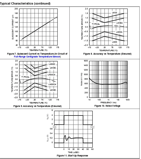
Typical Characteristics (continued)
200 180 160 140 120 100 80 60 40
–75 –25 25 75 TEMPERATURE (°C)
Figure 7. Quiescent Current vs Temperature (in Circuit of Full-Range Centigrade Temperature Sensor
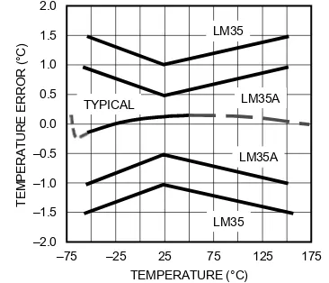
2.5 2.0 1.5 1.0 0.5 0.0 –0.5 –1.0 –1.5 –2.0 –2.5 TYPICAL
–75 –25 25 75 TEMPERATURE (°C)
Figure 9. Accuracy vs Temperature (Ensured)
TE M PE R AT U R E E R R O R (° C ) Q U IE SC EN T C U R R EN T (µ A) AUGUST 2016
Typical Characteristics (continued)
2.0 1.5 1.0 0.5 0.0 –0.5 –1.0 TYPICAL
125 175 (°C) C007
–1.5
–2.0
–75 –25 25 TEMPERATURE
Figure 7. Quiescent Current vs Temperature (in Circuit of
Range Centigrade Temperature Sensor) Figure 8. Accuracy vs Temperature (Ensured)
1600 LM35D LM35C LM35CA LM35CA LM35C 1400 1200 1000 800 600 400 200 0 125 175
(°C) C009
10 100
FREQUENCY
Temperature (Ensured) Figure 10. Noise
6 4 2 0 0.6 0.4 0.2 0
0 10 20 30 40 50 60 TIME (µSEC) C011
Figure 11. Start-Up Response VOU T (V ) VIN (V ) N ois e (n V/ H z) TE M PE R AT U R E E R R O R (° C ) www.ti.com LM35 LM35A LM35A LM35
25 75 125 175 TEMPERATURE (°C) C008
Figure 8. Accuracy vs Temperature (Ensured)
1k 10k 100k FREQUENCY (Hz) C010
www.ti.com
7 Detailed Description
Overview
The LM35-series devices are precision integrated
proportional to the Centigrade temperature. The LM35 device has an advantage over linear temp
calibrated in Kelvin, as the user is not required to subtract a large constant voltage from the output to obtain
convenient Centigrade scaling. The LM35 device does not require any external calibration or trimming to provide
typical accuracies of ± ¼ °C at room temperature and ± ¾ °C over a full
Lower cost is assured by trimming and calibration at the wafer level. The low output impedance, linear output,
and precise inherent calibration of the LM35 device m
easy. The device is used with single power supplies, or with plus and minus supplies. As the LM35 device draws
only 60
μ
A from the supply, it has very low self
operate over a −55°C to 150°C temperature range, while the LM35C device is rated for a −40°C to 110°C range
(−10° with improved accuracy). The temperature
The temperature-sensing element is then buffered by an amplifier and provided to the VOUT pin. The amplifier
has a simple class A output stage with typical 0.5
Diagram
. Therefore the LM35 can only source current and it's sinking capability is limited to 1
Functional Block Diagram
1.38 V
PTATnR1
nR1
Feature Description
LM35 Transfer Function
The accuracy specifications of the LM35 are given with respect to a simple linear transfer
V
OUT= 10 mv/°C × T
where
• V
OUTis the LM35 output voltage
• T is the temperature in °C
7.4 Device Functional Modes
The only functional mode of the LM35 is that it has an analog output directly proportional to temperature.
SNIS159G – AUGUSTseries devices are precision integrated-circuit temperature sensors, with an output voltage linearly
proportional to the Centigrade temperature. The LM35 device has an advantage over linear temp
calibrated in Kelvin, as the user is not required to subtract a large constant voltage from the output to obtain
convenient Centigrade scaling. The LM35 device does not require any external calibration or trimming to provide
ies of ± ¼ °C at room temperature and ± ¾ °C over a full −55°C to 150°C temperature range.
Lower cost is assured by trimming and calibration at the wafer level. The low output impedance, linear output,
and precise inherent calibration of the LM35 device makes interfacing to readout or control circuitry especially
easy. The device is used with single power supplies, or with plus and minus supplies. As the LM35 device draws
A from the supply, it has very low self-heating of less than 0.1°C in still air. The LM35 device is rated to
−55°C to 150°C temperature range, while the LM35C device is rated for a −40°C to 110°C range
−10° with improved accuracy). The temperature-sensing element is comprised of a delta
sensing element is then buffered by an amplifier and provided to the VOUT pin. The amplifier
has a simple class A output stage with typical 0.5-
Ω
output impedance as shown in the
. Therefore the LM35 can only source current and it's sinking capability is limited to 1
A1
Q1
Q2
10E
E
V
08.8 mVƒ˚C
i
+V
S+
A2
.125 R2
R2
The accuracy specifications of the LM35 are given with respect to a simple linear transfer
voltage
°C
The only functional mode of the LM35 is that it has an analog output directly proportional to temperature.
LM35
AUGUST 1999 – REVISED AUGUST 2016
circuit temperature sensors, with an output voltage linearly
proportional to the Centigrade temperature. The LM35 device has an advantage over linear temperature sensors
calibrated in Kelvin, as the user is not required to subtract a large constant voltage from the output to obtain
convenient Centigrade scaling. The LM35 device does not require any external calibration or trimming to provide
−55°C to 150°C temperature range.
Lower cost is assured by trimming and calibration at the wafer level. The low output impedance, linear output,
akes interfacing to readout or control circuitry especially
easy. The device is used with single power supplies, or with plus and minus supplies. As the LM35 device draws
air. The LM35 device is rated to
−55°C to 150°C temperature range, while the LM35C device is rated for a −40°C to 110°C range
sensing element is comprised of a delta-V BE architecture.
sensing element is then buffered by an amplifier and provided to the VOUT pin. The amplifier
output impedance as shown in the
Functional Block
. Therefore the LM35 can only source current and it's sinking capability is limited to 1
μ
A.
V
OUT= 10 mVƒ˚C
.125 R2
R2
The accuracy specifications of the LM35 are given with respect to a simple linear transfer function:
(1)
LM35
SNIS159G – AUGUST 1999 – REVISED AUGUST 2016
HEAVY
2 k
OUT
LM35
8 Application and Implementation
Information in the following applications sections is not part of the TI component
specification, and TI does not warrant its accuracy or completeness. TI’s customers are
responsible for determining suitability of components for their purposes. Customers should
validate and test their design implementation to confirm system functionality.
Application Information
The features of the LM35 make it suitable for many general temperature sensing applications. Multiple package
options expand on it's flexibility.
Capacitive Drive Capability
Like most micropower circuits, the LM35 device has a limited ability to drive heavy capacitive loads. Alone, the
LM35 device is able to drive 50 pF without special precautions. If heavier loads are anticipated, isolating or
decoupling the load with a resistor is easy (see
series R-C damper from output to ground (see
When the LM35 device is applied with a 200
device is relatively immune to wiring capacitance because the capacitance forms a bypass from ground
and not on the output. However, as with any linear circuit connected to wires in a hostile environment,
performance is affected adversely by intense electromagnetic sources (such as relays, radio transmitters, motors
with arcing brushes, and SCR transients), because the wiring acts as a receiving antenna and the internal
junctions act as rectifiers. For best results in such cases, a bypass capacitor from V
damper, such as 75
Ω
in series with 0.2 or 1
Figure 13
,
Figure 24
, and
Figure 25
.
+
—
Figure 12. LM35 with Decoupling from Capacitive Load
0.01 F BYPASS OPTONAL
AUGUST 2016
+ HEAVY CAPACITIVE LOAD, WIRING, ETC.
LM35 OUT
— 75
1 F
HEAVY CAPACITIVE LOAD, WIRING, ETC.
k
Implementation
NOTE
in the following applications sections is not part of the TI component
specification, and TI does not warrant its accuracy or completeness. TI’s customers are
responsible for determining suitability of components for their purposes. Customers should
ate and test their design implementation to confirm system functionality.
The features of the LM35 make it suitable for many general temperature sensing applications. Multiple package
Like most micropower circuits, the LM35 device has a limited ability to drive heavy capacitive loads. Alone, the
LM35 device is able to drive 50 pF without special precautions. If heavier loads are anticipated, isolating or
load with a resistor is easy (see
Figure 12
). The tolerance of capacitance can be improved with a
C damper from output to ground (see
Figure 13
).
When the LM35 device is applied with a 200-
Ω
load resistor as shown in
Figure 16
,
device is relatively immune to wiring capacitance because the capacitance forms a bypass from ground
and not on the output. However, as with any linear circuit connected to wires in a hostile environment,
performance is affected adversely by intense electromagnetic sources (such as relays, radio transmitters, motors
transients), because the wiring acts as a receiving antenna and the internal
junctions act as rectifiers. For best results in such cases, a bypass capacitor from V
INin series with 0.2 or 1
μ
F from output to ground, are often useful. Examples are shown in
TO
A
HIGH
−IMP
Figure 12. LM35 with Decoupling from Capacitive Load
TO A HIGH
Figure 13. LM35 with R-C Damper
www.ti.com
in the following applications sections is not part of the TI component
specification, and TI does not warrant its accuracy or completeness. TI’s customers are
responsible for determining suitability of components for their purposes. Customers should
ate and test their design implementation to confirm system functionality.
The features of the LM35 make it suitable for many general temperature sensing applications. Multiple package
Like most micropower circuits, the LM35 device has a limited ability to drive heavy capacitive loads. Alone, the
LM35 device is able to drive 50 pF without special precautions. If heavier loads are anticipated, isolating or
). The tolerance of capacitance can be improved with a
,
Figure 17
, or
Figure 19
, the
device is relatively immune to wiring capacitance because the capacitance forms a bypass from ground to input
and not on the output. However, as with any linear circuit connected to wires in a hostile environment,
performance is affected adversely by intense electromagnetic sources (such as relays, radio transmitters, motors
transients), because the wiring acts as a receiving antenna and the internal
IN
to ground and a series R-C
ground, are often useful. Examples are shown in
IMPEDANCE
LOAD
Figure 12. LM35 with Decoupling from Capacitive Load
www.ti.com
Typical Application
Basic Centigrade Temperature
Figure 14. Basic Centigrade Temperature Sensor (2 °C to 150 °C)
Design Requirements
Accuracy at 25°C Accuracy from
Temperature Slope
Detailed Design Procedure
Because the LM35 device is a simple temperature sensor that provides an analog output, design requirements
related to layout are more important than electrical requirements. For a detailed description, refer to the
Application Curve
Figure 15.
SNIS159G – AUGUST
LM35
Sensor
+V
S(4 V to 20 V)
OUTPUT
0 mV + 10.0 mVƒ˚C
Figure 14. Basic Centigrade Temperature Sensor (2 °C to 150 °C)
Table 1. Design Parameters
PARAMETER VALUE
Accuracy at 25°C ±0.5°C
Accuracy from –55 °C to 150°C ±1°C
Temperature Slope 10 mV/°C
Because the LM35 device is a simple temperature sensor that provides an analog output, design requirements
related to layout are more important than electrical requirements. For a detailed description, refer to the
Figure 15. Accuracy vs Temperature (Ensured)
2.0
1.5 LM35
1.0
0.5
TYPICAL LM35A
0.0
–0.5 LM35A
–1.0
–1.5
LM35 –2.0
–75 –25 25 75 125 175
TEMPERATURE (°C) C008
TE
M
PERA
TUR
E
ERRO
R
(°
C)
LM35
AUGUST 1999 – REVISED AUGUST 2016
Figure 14. Basic Centigrade Temperature Sensor (2 °C to 150 °C)
Because the LM35 device is a simple temperature sensor that provides an analog output, design requirements
LM35
SNIS159G – AUGUST 1999 – REVISED AUGUST 2016
1N914
18
10%
LM35
LM35
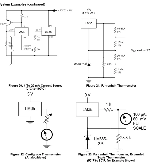
8.3 System Examples
5 V +
VOUT = 10
6.8 k 5% + 200 1% — FROM HEAT FINS — OUT 200 1% TWISTED
Figure 16. Two-Wire Remote Temperature Sensor
(Grounded Sensor)
+V
SFigure 18. Temperature Sensor, Single Supply
(−55° to +150°C)
AUGUST 2016
+
18 k
10%
10 mVƒ˚C (TAMBIENT = 1 ˚C)
HEAT
FINS
+
LM35
OUT
+ 2 ˚C TO + 40 ˚C
—
6.8 k
200
1%
TWISTED PAIR
5%
OR 10K RHEOSTAT
FOR GAIN ADJUST
Wire Remote Temperature Sensor
(Grounded Sensor)
Figure 17. Two-Wire Remote Temperature Sensor
(Output Referred to Ground)
0.01 F BYPASS OPTIONAL + OUT 2 k 1%
V
OUT—
Figure 18. Temperature Sensor, Single Supply
−55° to +150°C)
Figure 19. Two-Wire Remote Temperature Sensor
(Output Referred to Ground)
LM35 www.ti.com
5 V
TWISTED PAIR
200
1%
V
OUT= 10 mVƒ˚C (T
AMBIENT= 1 ˚C)
FROM + 2 ˚C TO + 40 ˚C
200
1%
Wire Remote Temperature Sensor
(Output Referred to Ground)
5 V
200 1%
TWISTED PAIR
VOUT = 10 mVƒ˚C (TAMBIENT = 10 ˚C)
FROM − 5 ˚C TO + 40 ˚C 2 k 200
1% 1%
www.ti.com
LM35
System Examples (continued)
4.7 k
2N2907
OUT
62.5 0.5%
+
—
OFFSET ADJUST
OUT
402 1%
50
LM317
Figure 20. 4-To-20 mA Current Source
(0°C to 100°C)
5 V
Figure 22. Centigrade Thermometer
(Analog Meter)
LM35
SNIS159G – AUGUST
LM385-
2.5
LM35
18 kK LM35
+ 5 V TO + 30 V +VS
(6 V to 20 V)
IN
LM317
ADJ
LM385−1.2
20 mA Current Source
Figure 21. Fahrenheit Thermometer
9 V
1 k
Figure 22. Centigrade Thermometer
Figure 23. Fahrenheit Thermometer, Expanded
Scale Thermometer
(50°F to 80°F, for Example Shown)
LM35
AUGUST 1999 – REVISED AUGUST 2016
25.5 k
45.5 kK 1%
10 kK 1%
26.4 kK 1% kK
1 MK 1%
VOUT = +1 mVƒ˚F
Figure 21. Fahrenheit Thermometer
1 k
100 µA,
60 mV
FULL-
SCALE
Figure 23. Fahrenheit Thermometer, Expanded
Scale Thermometer
LM35
SNIS159G – AUGUST 1999 – REVISED AUGUST 2016
˚F
20 k
67 68 69 70 71 72 73 74 75 76 77 78 79 80 81 82 83 84 85 86 +
20 F
18 10 18
LM3914
1 2 3 4 5 6 7 8 9 1 2 3 4 5 6 7 8
7 V 1.2 k*
+ VA
OUT VC
200* 499*
1.5 k*
+
1 F 1.5 k* R C
1 k
RA 1 k LM35
System Examples (continued)
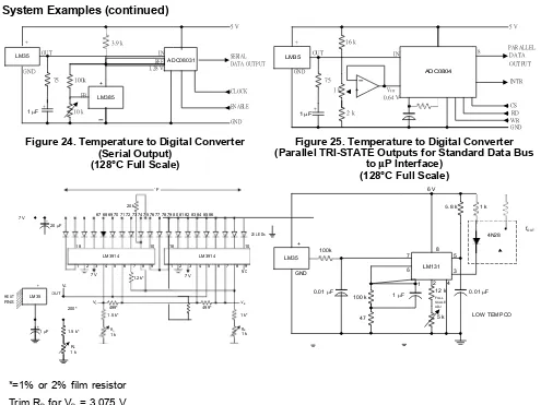
Figure 24. Temperature to Digital Converter
(Serial Output)
(128°C Full Scale)
7 V
HEAT FINS
*=1% or 2% film resistor
Trim R
Bfor V
B= 3.075 V
Trim R
Cfor V
C= 1.955 V
Trim R
Afor V
A= 0.075 V + 100 mV/°C ×T
Example, V
A= 2.275 V at 22°C
Figure 26. Bar-Graph Temperature Display
(Dot Mode)
+ 3.9 k
OUT IN
GND 1.28 V
75 100k + FB +
1 F 10 k
LM35 ADC08031
REF
LM385
AUGUST 2016
68 69 70 71 72 73 74 75 76 77 78 79 80 81 82 83 84 85 86
18 10
LM3914
1 2 3 4 5 6 7 8 9 NC 7 V VB 499* 1 k* RB 1 k + 100 k LM35 GND
100 k 1 F 0.01 F
47 5 V SERIAL DATA OUTPUT + LM35 GND OUT 75 16 k IN CLOCK ENABLE GND
1 F +
1 k +
2 k
VREF
0.64 V
Temperature to Digital Converter
(128°C Full Scale)
Figure 25. Temperature to Digital Converter
(Parallel TRI-STATE Outputs for Standard Data Bus
to
μ
P Interface)
(128°C Full Scale)
20 LEDs
= 0.075 V + 100 mV/°C ×T
ambientGraph Temperature Display
Figure 27. LM35 With Voltage
Converter and Isolated Output
(2°C to 150°C; 20 to 1500 Hz)
ADC08031
www.ti.com
6.8 k 1 k
4N28 8
7 5
6 LM131 3
1 F 2 12 k FULL SCALE ADJ 4
0.01 F
5 k LOW TEMPCO
5 V ADC0804 PARALLEL 8 DATA OUTPUT INTR CS RD WR GND
Figure 25. Temperature to Digital Converter
STATE Outputs for Standard Data Bus
P Interface)
(128°C Full Scale)
6 V
fOUT
Figure 27. LM35 With Voltage-To-Frequency
Converter and Isolated Output
www.ti.com
9 Power Supply Recommendations
The LM35 device has a very wide 4
applications. In noisy environments, TI recommends adding a 0.1
supply voltage. Larger capacitances maybe required and are dependent on the power
10 Layout
Layout Guidelines
The LM35 is easily applied in the same way as other integrated
device to a surface and the temperature should be within about 0.01°C of the surface temperature.
The 0.01°C proximity presumes that the ambient air temperature is almost the same as the surface temperature.
If the air temperature were much higher or lower than the surface temperature, the actual temperature of the
LM35 die would be at an intermediate
this is especially true for the TO-92 plastic package. The copper leads in the TO
thermal path to carry heat into the device, so its temperature might be cl
surface temperature.
Ensure that the wiring leaving the LM35 device is held at the same temperature as the surface of interest to
minimize the temperature problem. The easiest fix is to cover up these wires with a be
bead will ensure that the leads and wires are all at the same temperature as the surface, and that the
temperature of the LM35 die is not affected by the air
The TO-46 metal package can also be soldered to a metal surfa
case the V− terminal of the circuit will be grounded to that metal. Alternatively, mount the LM35 inside a sealed
end metal tube, and then dip into a bath or screw into a threaded hole in a tank. As with any I
and accompanying wiring and circuits must be kept insulated and dry, to avoid leakage and corrosion. This is
especially true if the circuit may operate at cold temperatures where condensation can occur. Printed
coatings and varnishes such as a conformal coating and epoxy paints or dips are often used to insure that
moisture cannot corrode the LM35 device or its
These devices are sometimes soldered to a small light
speed up the response in slowly-moving air. On the other hand, a small thermal mass may be added to the
sensor, to give the steadiest reading despite small deviations in the air temperature.
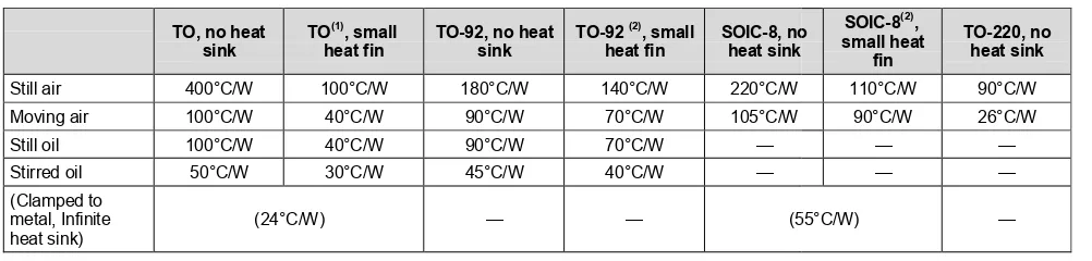
Table 2. Temperature Rise of LM35 Due To Self
TO, no heat
sink TO
(1), small
heat fin
Still air 400°C/W 100°C/W
Moving air 100°C/W 40°C/W
Still oil 100°C/W 40°C/W
Stirred oil 50°C/W 30°C/W
(Clamped to metal, Infinite
heat sink) (24°C/W)
(1) Wakefield type 201, or 1-in disc of 0.02-in sheet brass, soldered to case, or (2) TO-92 and SOIC-8 packages glued and
SNIS159G – AUGUST
Recommendations
The LM35 device has a very wide 4-V to 30-V power supply voltage range, which makes it ideal for many
applications. In noisy environments, TI recommends adding a 0.1
μ
F from V+ to GND to bypass the power
supply voltage. Larger capacitances maybe required and are dependent on the power
The LM35 is easily applied in the same way as other integrated-circuit temperature sensors. Glue or cement the
and the temperature should be within about 0.01°C of the surface temperature.
The 0.01°C proximity presumes that the ambient air temperature is almost the same as the surface temperature.
If the air temperature were much higher or lower than the surface temperature, the actual temperature of the
LM35 die would be at an intermediate temperature between the surface temperature and the air temperature;
92 plastic package. The copper leads in the TO-92 package are the principal
thermal path to carry heat into the device, so its temperature might be closer to the air temperature than to the
Ensure that the wiring leaving the LM35 device is held at the same temperature as the surface of interest to
minimize the temperature problem. The easiest fix is to cover up these wires with a be
bead will ensure that the leads and wires are all at the same temperature as the surface, and that the
temperature of the LM35 die is not affected by the air temperature.
46 metal package can also be soldered to a metal surface or pipe without damage. Of course, in that
− terminal of the circuit will be grounded to that metal. Alternatively, mount the LM35 inside a sealed
end metal tube, and then dip into a bath or screw into a threaded hole in a tank. As with any I
and accompanying wiring and circuits must be kept insulated and dry, to avoid leakage and corrosion. This is
especially true if the circuit may operate at cold temperatures where condensation can occur. Printed
shes such as a conformal coating and epoxy paints or dips are often used to insure that
moisture cannot corrode the LM35 device or its connections.
These devices are sometimes soldered to a small light-weight heat fin to decrease the thermal time constant
moving air. On the other hand, a small thermal mass may be added to the
sensor, to give the steadiest reading despite small deviations in the air temperature.
Table 2. Temperature Rise of LM35 Due To Self-heating (Thermal Resistance, R
, small
heat fin TO-92, no heat sink TO-92
(2), small
heat fin SOIC-8, noheat sink
100°C/W 180°C/W 140°C/W 220°C/W
40°C/W 90°C/W 70°C/W 105°C/W
40°C/W 90°C/W 70°C/W —
30°C/W 45°C/W 40°C/W —
— — (55°C/W)
in sheet brass, soldered to case, or similar.
leads soldered to 1-in square of 1/16-in printed circuit board with
LM35
AUGUST 1999 – REVISED AUGUST 2016
V power supply voltage range, which makes it ideal for many
F from V+ to GND to bypass the power
supply voltage. Larger capacitances maybe required and are dependent on the power-supply noise.
circuit temperature sensors. Glue or cement the
and the temperature should be within about 0.01°C of the surface temperature.
The 0.01°C proximity presumes that the ambient air temperature is almost the same as the surface temperature.
If the air temperature were much higher or lower than the surface temperature, the actual temperature of the
temperature between the surface temperature and the air temperature;
92 package are the principal
oser to the air temperature than to the
Ensure that the wiring leaving the LM35 device is held at the same temperature as the surface of interest to
minimize the temperature problem. The easiest fix is to cover up these wires with a bead of epoxy. The epoxy
bead will ensure that the leads and wires are all at the same temperature as the surface, and that the
ce or pipe without damage. Of course, in that
− terminal of the circuit will be grounded to that metal. Alternatively, mount the LM35 inside a sealed-
end metal tube, and then dip into a bath or screw into a threaded hole in a tank. As with any IC, the LM35 device
and accompanying wiring and circuits must be kept insulated and dry, to avoid leakage and corrosion. This is
especially true if the circuit may operate at cold temperatures where condensation can occur. Printed-circuit
shes such as a conformal coating and epoxy paints or dips are often used to insure that
weight heat fin to decrease the thermal time constant and
moving air. On the other hand, a small thermal mass may be added to the
al Resistance, R
θJA) 8, no small heat SOIC-8(2),fin
TO-220, no heat sink 110°C/W 90°C/W
90°C/W 26°C/W
— —
— —
(55°C/W) —
LM35
SNIS159G – AUGUST 1999 – REVISED AUGUST 2016
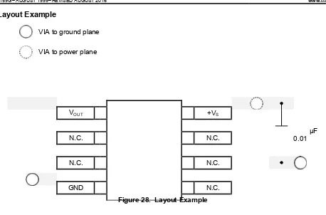
Layout Example
VIA to ground plane
VIA to power plane
V
OUTN.C.
N.C.
GND
AUGUST 2016plane
Figure 28. Layout Example
+V
SN.C.
N.C.
N.C.
www.ti.com
www.ti.com
11 Device and Documentation
Receiving Notification of Documentation
To receive notification of documentation updates, navigate to the device product folder on ti.com. In the upper
right corner, click on A
lert me
to register and receive a weekly digest of any product information that has
changed. For change details, review the revisi
Community Resources
The following links connect to TI community resources. Linked contents are provided "AS IS" by the respective
contributors. They do not constitute TI specifications and do not necessarily ref
Use
.
TI E2E™ Online Community
TI's Engineer
among engineers. At e2e.ti.com, you can ask questions, share knowledge, explore ideas and help
solve problems with fellow engineers.
Design Support
TI's Design Support
contact information for technical support.
Trademarks
E2E is a trademark of Texas Instruments.
All other trademarks are the property of their respective owners.
Electrostatic Discharge Caution
These devices have limited built-in ESD protection. The leads should be shorted together or the device placed in conductive foam during storage or handling to prevent electrostatic damage to the MOS gates.
Glossary
SLYZ022
—
TI Glossary
.
This glossary lists and explains terms, acronyms, and definitions.
12 Mechanical, Packaging, and Orderable
The following pages include mechanical, packaging, and orderable informat
current data available for the designated devices. This data is subject to change without notice and revision of
this document. For browser-based versions of this data sheet, refer to the left
SNIS159G – AUGUST
Device and Documentation Support
Receiving Notification of Documentation Updates
notification of documentation updates, navigate to the device product folder on ti.com. In the upper
to register and receive a weekly digest of any product information that has
changed. For change details, review the revision history included in any revised document
The following links connect to TI community resources. Linked contents are provided "AS IS" by the respective
contributors. They do not constitute TI specifications and do not necessarily reflect TI's views; see TI's
TI's Engineer-to-Engineer (E2E) Community.
Created to foster collaboration
among engineers. At e2e.ti.com, you can ask questions, share knowledge, explore ideas and help
solve problems with fellow engineers.
TI's Design Support
Quickly find helpful E2E forums along with design support tools and
contact information for technical support.
E2E is a trademark of Texas Instruments.
All other trademarks are the property of their respective owners.
Caution
in ESD protection. The leads should be shorted together or the device placed in conductive foam during storage or handling to prevent electrostatic damage to the MOS gates.
This glossary lists and explains terms, acronyms, and definitions.
Mechanical, Packaging, and Orderable Information
The following pages include mechanical, packaging, and orderable information. This information is the most
current data available for the designated devices. This data is subject to change without notice and revision of
based versions of this data sheet, refer to the left-hand navigation.
LM35
AUGUST 1999 – REVISED AUGUST 2016
notification of documentation updates, navigate to the device product folder on ti.com. In the upper
to register and receive a weekly digest of any product information that has
document
The following links connect to TI community resources. Linked contents are provided "AS IS" by the respective
lect TI's views; see TI's
Terms of
Created to foster collaboration
among engineers. At e2e.ti.com, you can ask questions, share knowledge, explore ideas and help
Quickly find helpful E2E forums along with design support tools and
in ESD protection. The leads should be shorted together or the device placed in conductive foam
ion. This information is the most
current data available for the designated devices. This data is subject to change without notice and revision of
PACKAGE OPTION ADDENDUM
www.ti.com 17-Mar-2017
PACKAGING INFORMATION
Orderable Device Status
(1)
Package Type Package
Drawing Pins Package Qty Eco Plan (2)
Lead/Ball Finish
(6)
MSL Peak Temp
(3)
Op Temp (°C) Device Marking
(4/5)
Samples
LM35AH ACTIVE TO NDV 3 500 TBD Call TI Call TI -55 to 150 ( LM35AH ~ LM35AH)
LM35AH/NOPB ACTIVE TO NDV 3 500 Green (RoHS
& no Sb/Br) Call TI Level-1-NA-UNLIM -55 to 150 ( LM35AH ~ LM35AH)
LM35CAH ACTIVE TO NDV 3 500 TBD Call TI Call TI -40 to 110 ( LM35CAH ~
LM35CAH)
LM35CAH/NOPB ACTIVE TO NDV 3 500 Green (RoHS
& no Sb/Br) Call TI Level-1-NA-UNLIM -40 to 110 ( LM35CAH ~ LM35CAH) LM35CAZ/LFT4 ACTIVE TO-92 LP 3 2000 Green (RoHS
& no Sb/Br) CU SN N / A for Pkg Type LM35 CAZ LM35CAZ/NOPB ACTIVE TO-92 LP 3 1800 Green (RoHS
& no Sb/Br) CU SN N / A for Pkg Type -40 to 110 LM35 CAZ
LM35CH ACTIVE TO NDV 3 500 TBD Call TI Call TI -40 to 110 ( LM35CH ~ LM35CH)
LM35CH/NOPB ACTIVE TO NDV 3 500 Green (RoHS
& no Sb/Br) Call TI Level-1-NA-UNLIM -40 to 110 ( LM35CH ~ LM35CH) LM35CZ/LFT1 ACTIVE TO-92 LP 3 2000 Green (RoHS
& no Sb/Br) CU SN N / A for Pkg Type LM35 CZ LM35CZ/NOPB ACTIVE TO-92 LP 3 1800 Green (RoHS
& no Sb/Br) CU SN N / A for Pkg Type -40 to 110 LM35 CZ
LM35DH ACTIVE TO NDV 3 1000 TBD Call TI Call TI 0 to 70 ( LM35DH ~ LM35DH)
LM35DH/NOPB ACTIVE TO NDV 3 1000 Green (RoHS
& no Sb/Br) Call TI | POST-PLATE Level-1-NA-UNLIM 0 to 70 ( LM35DH ~ LM35DH)
LM35DM NRND SOIC D 8 95 TBD Call TI Call TI 0 to 100 LM35D
M
LM35DM/NOPB ACTIVE SOIC D 8 95 Green (RoHS
& no Sb/Br) CU