Preliminary Testing Tool for VGA Monitor Using FPGA XC4005XL and
XS-Board
Indar Sugiarto
Department of Electrical Engineering - Petra Christian University Jl. Siwalankerto 121-131, Surabaya 60236
Email: [email protected]
Abstract
There are a lot of factors causing the monitor not to work well. Examination by the technician generally involves two steps: preliminary testing for facts finding and minor problems solving, and/or followed by further hardware-repairing. This paper describes the using of XS-Board and the Xilinx-FPGA within it to create preliminary testing tool for VGA troubleshooting. The goal of this research is to evaluate how effective the using of XS-Board with FPGA XC4005XL to implement a preliminary testing tool for VGA troubleshooting. The system will generate pictures in certain patterns and colors periodically to help technician in observing the monitor. The experiment shows that XS-Board with FPGA XC4005XL inside it is capable in handling the signaling for VGA monitor to display 64 colors almost fullscreen. With only consume 15% of logic cell resources; this system is efficient enough and ready to be improved further. One of its critical characteristics is that the internal clock generator of XC4005XL has 10% tolerant in frequency variation resulting in imperfect display of fullscreen mode.
Keyword: VGA monitor, FPGA
Abstrak
Ada banyak faktor penyebab kenapa monitor tidak berfungsi dengan baik. Pemeriksaan oleh tukang servis biasanya meliputi dua tahap: pemeriksaan pendahuluan untuk mencari fakta teknis dan menyelesaikan kerusakan kecil, dan/atau dilanjutkan dengan perbaikan perangkat keras lebih lanjut. Makalah ini menjelaskan penggunaan XS-Board yang dilengkapi dengan FPGA dari Xilinx untuk menciptakan perlengkapan pemeriksaan pendahuluan untuk perawatan VGA. Tujuan penelitian ini adalah untuk mengetahui seberapa efektif penggunaan XS-Board dengan FPGA XC4005 di dalamnya guna mengimplementasikan sebuah alat pemeriksa awal untuk perbaikan monitor VGA. Metode yang dilakukan adalah dengan membangkitkan gambar menggunakan pola-pola dan warna tertentu secara periodik untuk membantu tukang servis dalam pemeriksaan. Percobaan menunjukkan bahwa XS-Board dengan XC4005XL di dalamnya mampu menghasilkan sinyal-sinyal kontrol untuk VGA sehingga mampu menampilkan hingga 64 warna dengan tampilan layar hampir penuh (fullscreen). Dengan hanya menggunakan 15% dari sumberdaya FPGA yang tersedia, sistem ini dirasa cukup efisien dan bisa dikembangkan lagi lebih lanjut. Salah satu karakteristik penting dari sistem ini adalah pembangkit clock internal dari XC4005XL yang memiliki toleransi variasi frekuensi hingga 10% yang mengakibatkan tampilan yang tidak benar-benar layah penuh.
Kata kunci: monitor VGA, FPGA
Introduction
All computers need a video system to display the text, graphics, and multimedia images associated with everyday computing. A video system generally consists of two elements – the video controller and the monitor. Most desktop video systems use a cathode ray tube (CRT) as their monitor. The VGA (Video Graphics Array) and its descendant (SVGA or Super VGA) is the most accepted technology for the PC’s (Personal Computer) monitor nowadays.
There are a lot of factors causing the monitor not to work well. Some of them are easily identified by their symptoms, especially when we use Windowstm
Note: Discussion is expected before December, 1st 2005. The proper discussion will be published in Electrical Engineering Journal volume 6, number 1, March 2006.
Operating System, and the rest are left for the technician to deal with. Examination by the technician generally involves two steps: preliminary testing for facts finding and minor problems solving, and/or followed by further hardware-repairing.
This paper describes the using of XS-Board and the Xilinx-FPGA within it to create preliminary testing tool for VGA troubleshooting. The order of this manuscript is arranged firstly by introducing VGA technology and XS-Board system, and then followed by HDL design, implementation, analyzing and closed by conclusions.
VGA Monitor
PCs[3]. It is VGA that provides the familiar 640 x 480 x 16 screen mode which has become the baseline for Microsoft Windows 9x/Me/XP “Safe Mode” display. The use of analog color signals allows VGA systems to produce a palette of 16 colors from 262.144 possible colors. The video adapter in PC sends the signals from its image memory at fixed rate (usually configurable) through the DAC (digital to analog converter) circuit to the monitor connector on the graphics card. The DAC converts numeric pixel color values to voltage levels for red, green, and blue which are sent to monitor through the monitor cable.
Figure 1 is the representation of connector usually found in the VGA monitor. There are three signals - red, green, and blue - that send color information to the monitor. These three signals each drive an electron gun that emits electrons which paint one primary color at a point on the monitor screen. Analog levels between 0 (completely dark) and 0.7 V (maximum brightness) on these control lines tell the monitor what intensities of these three primary colors to combine to make the color of a dot (or pixel) on the monitor’s screen.
Pinouts 1 2 3 4 5 6 7 8
Red out Green out Blue out Monitor ID2 Ground Red return Green return Blue return
9 10 11 12 13 14 15
no pin Sync return Monitor ID0 Monitor ID1 Horizonal Sync Vertical Sync Monitor ID3
Figure 1. The DB15 VGA connector [1]
Each analog color input can be set to one of four levels by two digital outputs using a simple two-bit digital-to-analog converter (see Figure 2). The four possible levels on each analog input are combined by the monitor to create a pixel with one of 4 x 4 x 4 = 64 different colors. So the six digital control lines let us select from a palette of 64 colors.
A horizontal line consists of several pixels and a frame composed of multiple lines which can present an image on the monitor screen. A frame of VGA video typically has 480 lines and each line usually
contains 640 pixels. In order to paint a frame, there are deflection circuits in the monitor that move the electrons emitted from the guns both left-to-right and top-to-bottom across the screen. These deflection circuits require two synchronization signals in order to start and stop the deflection circuits at the right times so that a line of pixels is painted across the monitor and the lines stack up from the top to the bottom to form an image. The timing for the VGA synchronization signals is shown in Figure 3 [2].
Figure 2. Digital to analog VGA monitor interface[2]
Negative pulses on the horizontal sync signal mark the start and end of a line and ensure that the monitor displays the pixels between the left and right edges of the visible screen area. The actual pixels are sent to the monitor within a 25.17 µs window. The horizontal sync signal drops low a minimum of 0.94 µs after the last pixel and stays low for 3.77 µs. A new line of pixels can begin a minimum of 1.89 µs after the horizontal sync pulse ends. So a single line occupies 25.17 µs of a 31.77 µs interval. The other 6.6 µs of each line is the horizontal blanking interval during which the screen is dark.
In an analogous fashion, negative pulses on a vertical sync signal mark the start and end of a frame made up of video lines and ensure that the monitor displays the lines between the top and bottom edges of the visible monitor screen. The lines are sent to the monitor within a 15.25 ms window. The vertical sync signal drops low a minimum of 0.45 ms after the last line and stays low for 64 µs. The first line of the next frame can begin a minimum of 1.02 ms after the vertical sync pulse ends. So a single frame occupies 15.25 ms of a 16.784 ms interval. The other 1.534 ms of the frame interval is the vertical blanking interval during which the screen is dark.
Xilinx FPGA and XS-Board
FPGA (Field Programmable Gate Array) is a type of Programmable Logic Device which has regular structure of logic cells or modules and interconnects. The internal structure of this device is arranged so that the FPGA has high flexibility in design and configuration. Our project is carried on FPGA XC4005XL from Xilinx. XC4005XL has 196 CLBs (Configurable Logic Block) which is adequate to implement logic system equivalent with 5000 logic gates. It also has internal clock with frequencies vary from 15 Hz to 8 MHz.
XS-Board is a prototyping board for PLD-based application made by Xess Corporation. Depending on what PLD is used; XS-Board may vary from the simple one to the most complex system. In this project, we use XS-Board for Xilinx FPGA which is called XS-40. Figure 4 shows interconnect diagram within XS-40 featuring XC4005XL FPGA.
The PC can transmit signals to the XS40 Board through the eight data output bits of the parallel port. The FPGA has direct access to these signals. Special bits are used to download configuration bits and to set mode of the FPGA. These pins are pins 1, 7, 8, 14, and 17 of the parallel port. JTAG method is used
to download the FPGA bitstreams through these pins. Communication from the XS40 Board back to the PC also occurs through the parallel port. The PC can read the status pins to fetch data from the XS40 Board.
Figure 4. Interconnect diagram within XS-40. [4]
The FPGA also has access to the VGA monitor through connector attached on the board. The XS Board can drive the active-low horizontal and vertical sync signals that control the width and height of the video frame. The XS Board also has access to two bits each of red, green, and blue color signals so it can generate pixels in any of 22×22×22=64 different colors. The following listing shows pins connections between XS-Board and the VGA lines.
HDL Design
HDL (Hardware Description Language) is used by system designers whenever they want to implement any circuit or system onto single chip. This language differs from common computer programming language in such method that the algorithm is device oriented. It means that the procedure to implement the algorithm must confirm the technology used by the device. We use VHDL (Very High Speed Integrated Circuit Hardware Description Language) to implement the algorithm. The following step is used to implement HDL on XS-Board for our project.
Figure 5. Design flow of preliminary testing for VGA monitor project.
The project of preliminary testing tool for VGA monitor is working as follows. The FPGA through XS-Board is responsible for transmitting control signals to VGA monitor so that the monitor will display several colors for entire viewable area of the screen. One of our goals is to examine how many colors are generated for full-screen display in VGA monitor using XC4005XL. The color of monitor is changed periodically to test monitor respond for specific color. By adjusting the color displaying rate, it may give us a “glowing” monitor. The technician may discover any monitor defects by this method.
The following lines are the algorithm for our project.
/* send L lines of video to the monitor */ for line_cnt=1 to L
/* L is equivalent to maximum number of rows */
/* send P pixels for each line */ for pixel_cnt=1 to P
/* P is equivalent to maximum number of columns */
send color to monitor color = color + 1 d = d + 1
/* blank the monitor for H pixels */ for horiz_blank_cnt=1 to H
color = BLANK
send color to monitor
/* pulse the horizontal sync at the right time */
horiz_blank_cnt= horiz_blank_cnt + 1 line_cnt = line_cnt + 1
/* blank the monitor for V lines and insert vertical sync */
for vert_blank_cnt=1 to V color = BLANK
send color to monitor
/* pulse the vertical sync at the right time */
vert_blank_cnt = vert_blank_cnt + 1 /* go back to the start process */
Experiment and Testing
The most critical issue in this project is signal period for driving the R, G, B, horizontal and vertical synchronization signals. According to the standard, all signals have their maximum values so that the CRT will work well. So, the deepest concern of our project lies on its frequency clock. Because we used the internal clock of the XC4005XL (OSC4), we examined firstly to the actual frequency generated by XC4005XL. Adverse ambient temperature and other external noise may degrade original frequency of this FPGA. Figure-6 below shows how we examined the actual frequency of XC4005XL and table-1 summa-rizes the actual frequencies emitted by internal clock generator (which are passed through pins 80 to 84 of XC4005XL).
Figure 6. Clock generator using component OSC4 Design entry via VHDL
language.
Creating netlist by synthesize procedure
FPGA bitstreams generation by implementation procedure
Downloading bitstreams onto XS-Board using XSTOOLS
Table 1. Actual frequency output of OSC4
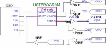
Significant degradation of clock frequency at the output pins of FPGA is due to the fact that the clock signal goes to the outside of FPGA through internal routing matrix and IOB. Originally, the internal clock frequency is intended for internal purpose only. Consequently, it affect the overall performance of the displayed screen like we show in the rest of this paper. The following picture (figure 7) shows the schematic of our project which is drawn in Xilinx Foundation 2.1i. The schematic representation of our project is looked simple because we carried out all programming in native language (VHDL).
Figure 7. Schematic representation of the project
After synthesize and implement the design within the compiler (Xilinx Foundation 2.1i), resulted bit-streams were downloaded onto the XS-Board using special software called XSTOOLS. The SVGA monitor was plugged onto the XS-Board and its response would be evaluated. The monitor displayed all 64 colors with interval 1 second for each color. It was also discovered small missing pixels on the screen; it’s about 0,5 cm width at right side viewable region of the screen. The following explanation can describe this phenomenon.
The frequency clock of about 8 MHz within the FPGA is used and its actual frequency may vary from 7,84 to 7,44 MHz. This clock sets the maximum rate at which pixels can be sent to the monitor. First, we assume that the applied frequency is about 7,8 Mhz, since it is not long after power on. So the pulse period of this clock is 1 / 7,8 MHz ≈ 0,13 µs. To occupy 31,77 µs of line period (between two consecutive horizontal blanking interval), it needs 31,77 / 0,13 ≈ 244 cycles. Using 8 bits counter, we got 256 cycles. If the applied frequency is about 7,6 MHz, we got pulse period of 1 / 7,4 Mhz ≈ 0,14 µs. So, it needs 31,77 / 0,14 ≈ 227 cycles for one line. Consequently, we waste 256 – 227 = 29 cycles. Using SVGA monitor with 0,28 dot pitch, we gain about 29 x 0,28 ≈ 8,12 mm blank area.
Each frame is composed by 528 video lines (only 480 are visible, the other 48 are blanked), so approximately a ten bit counter is needed for the line counter. A ten bit counter will count from 0 to 1024 whereas we need only 528 cycles. So, it was decided to use 9 bit counter for vertical synchronization.The counter is asynchronously set to zero when the reset input is high. The counter increments on the rising edge of the horizontal sync pulse after a line of pixels is completed. The range for the horizontal pixel counter is [0,511]. When the counter reaches 511, it rolls over to zero on the next cycle. Thus, the counter has a period of 512 lines. Since the duration of a line of pixels is 31,77 ms, this makes the frame interval equal to 16,266 ms, which less 0,52 ms from normal operation (16,78 ms). And again, we loose some pixels at the bottom of the screen. But this approach of using smaller bit counter, result in less FPGA resource was used.
Other useful information about our project is derived from implementation report of Xilinx Foundation 2.1i. Table 2 below shows resource utilization by the project using FPGA XC4005XL.
Table 2. Device utilization by the project.
Resource parameters Quantity
Number of External IOBs Flops
Most of the resources are used for counters. We use 4 counters in the design: 4 bit as frequency divider yielding 1 second clock pulse for color transition, 6 bit counter for color selection, 8 bit counter for horizontal blanking interval, and 9 bit counter for vertical blanking interval. It is obviously inferred from table 2 that the rest of resources are available for further improvement such as high resolution and true color system implementation.
Conclusion
From implementation and testing of the project, we conclude that:
9 Internal clock generator of XC4005XL may vary within 10% from its standard frequency. The frequency degrades significantly if it’s used to drive external I/O devices.
9 Blank area of the screen is caused by the mismatch of counter value with its correspondent blanking interval. Further improvement could be made by placing appropriate modulo-n counter as replacement for the binary counter.
This system still can be improved to accommodate the SVGA (Super Video Graphic Array) preliminary testing system. Of course, some modifications of the circuit must be made in order to acquire the require-ment for driving SVGA monitor. High resolution DAC and the high stability external clock circuit must be considered by this way.
References
[1] http://computer.howstuffworks.com/monitor.htm [2] “XStend Board V1.3 Manual”, Xess Corporation:
1999.
[3] Bigelow, Stephen J., “Bigelow’s PC Hardware Desk Reference”, McGraw-Hill/Osborner: 2003. [4] “XS40, XSP Board V1.4 User Manual”, Xess
Corporation: 1999.
![Figure 2. Digital to analog VGA monitor interface [2]](https://thumb-ap.123doks.com/thumbv2/123dok/3654671.1466341/2.595.289.488.203.503/figure-digital-to-analog-vga-monitor-interface.webp)
![Figure 4. Interconnect diagram within XS-40. [4]](https://thumb-ap.123doks.com/thumbv2/123dok/3654671.1466341/3.595.335.554.158.469/figure-interconnect-diagram-within-xs.webp)