136
Electrical Characteristics and Annealing Effect on Al/n-GaSb Schottky Diode
Doped Using DMTe (Dimethyltellurium)
Ari Handono Ramelan1), Harjana1), Pepen Arifin2) and Ewa Goldys3)
1)
Physics Department, Faculty of Mathematics and Natural Sciences Sebelas Maret University, (UNS) Surakarta, Indonesia.
2)
Physics Department, Faculty of Mathematics and Natural Sciences Institute of Technology Bandung, Bandung
3)
Physics Department, Faculty of Science and Engineering, Macquarie University - Sydney, Australia
e-mail: [email protected]
Received 19 September 2010, accepted for publication 11 October 2010
Abstract
The electrical properties of Al/n-GaSb Schottky diodes, doped with 1.4 × 1018 cm−3 (tellurium) were examined. C-V (capacitance-voltage) measurements at 300 K show barrier heights of 0.63 eV, compared to 0.59 eV determined from room temperature I-V (current-voltage) measurements. The voltage and frequency dependence on the capacitance is due to the ideality factor of the Schottky barrier and due to a high series resistance. At low frequency the measured capacitance is dominated by the depletion capacitance of the Al/n-GaSb Schottky diode which is bias-dependent and frequency-dependent. The diode shows a strong temperature dependence of ideality factor from approximately 3.6 at room temperature to as high as 6.7 at 140 K. There may be a small portion of the device nonideality attributable to generation-recombination currents due to deep levels in GaSb. The barrier height decreased from 0.57 eV to 0.35 eV for the sample annealed at 300oC for 1 minute.
Keywords: Schottky diode, Electrical properties, Annealing, Doping DMTe(Dimethyltellurium)
Abstrak
Sifat-sifat listrik dari diode Schottky Al/n-GaSb yang didadah dengan tellurium 1.4 × 1018 cm−3 dikaji dalam penelitian ini. Pengukuran C-V (kapasitansi-tegangan) pada suhu 300 K menunjukkan bahwa besarnya energi halang (barrier height) sebesar 0,63 dan dibandingkan dengan hasil pengukuran I-V (arus-tegangan) pada suhu kamar adalah sebesar 0,59 eV. Ketergantungan kapasitansi terhadap tegangan dan frekuensi adalah disebabkan oleh factor idealitas (ideality factor) energi halang dari diode Schottky dan juga disebabkan oleh resistansi seri yang tinggi. Pada frekuensi rendah kapasitansi yang terukur didominasi oleh kapasitansi deplesi dari diode Schottky Al/n-GaSb yang tergantung dari tegangan bias dan frekuensi. Faktor idealitas diode menunjukkan ketergantungan yang sangat kuat terhadap suhu, dari sekitar 3,6 pada suhu kamar sampai sebesar 6,7 untuk suhu 140o. Ketidak-idelan divais munculnya dari arus generasi-rekombinasi karena tingkatan energy dalam GaSb. Energi halangnya menurun dari 0,57 eV menjadi 0,35 eV untuk sampel dianil pada suhu 300oC selama 1 menit.
Kata kunci: Diode Schottky, Sifat listrik, Penganilan, Pendadahan DMTe(Dimethyltellurium)
1. Introduction
In a perfect metal-semiconductor contact, charge carriers can flow in either direction without experiencing any resistance at the interface. In reality, however, a potential barrier is always formed at the interface. The formation of the so called Schottky barrier has been modelled by several workers. The first model of the barrier formation was developed by Schottky (Schottky, 1938) and Mott (Mott, 1938). They suggested that, in the absence of interface states, the barrier is mainly due to the difference in the work function of the metal and semiconductor. When the metal is brought into contact with the semiconductor, in the case where the work function of the metal is larger than that of the semiconductor, electrons will be transferred from the semiconductor to the metal. The process will
continue until the Fermi levels of the two materials line up. This process leads to an energy band bending within the semiconductor, forming a space charge depletion region.
Schottky diodes obtained by evaporating various metals (Al, Au, Ag, Ni, Sb, Pd) on (100) n-GaSb (Te doped with density in the range of 1-2x1017 cm-3) have been reported (Milnes et al., 1993; Liu et al., 2004; Ahmetoglu et al., 2007) different barrier height values (depending also on the surface treatment) were found : for example, qφB ranges between 0.38-0.44, 0.64-0.84, and 0.43-0.46 eV, respectively, for silver, gold, and nickel deposited on vacuum cleaved GaSb. However, more recently it has been shown that pinning of the Fermi level near the top of the valence band (Dimoulas et al., 2006; Li et al., 2010) is responsible for an almost independent Schottky barrier height compared to the work function of the metal utilised (Polyakov et al., 1992; Ait Kaci et al., 2001). In fact, with a direct band gap equal to 0.7525 eV at 300 K, GaSb shows one of the highest Schottky barrier heights which deviates from the simple rule qφB = 2/3Eg (Mead,
1966). However, the achievement of an ideal GaSb Schottky barrier has proved to be difficult because an oxidised film inhomogeneously grows on the GaSb surfaces and if the latter is not stabilised by a passivating process, the oxide layer degrades the rectifying properties of any metal contact deposited on the surface. In fact, the highest barrier heights have been obtained on vacuum cleaved GaSb crystals (Pole et al., 1987; Walters and Williams, 1988) or by evaporating in situ Al metal contact on molecular beam epitaxy grown n-GaSb layers (Perotin et al., 1994).
In this paper, we investigate the electrical properties of Al/n-GaSb Te-doped epilayers grown by MOCVD and the effect of thermal treatment on the properties of the Schottky diodes.
2. Experimental Details
2.1 Device Fabrication
n-GaSb Te-doped epilayers were grown in a horizontal quartz atmospheric pressure MOCVD reactor. Six IR lamps were used to heat the graphite susceptor. TMGa (trimethylgallium) and TMSb (trimethylantimony) were used as metalorganic sources and kept at a constant bath temperature of -9 and 0oC, respectively which correspond to a molar flow of 2.53 and 1.82 µmol/min respectively, for 1 sccm hydrogen flows through the metalorganics. DMTe (dimethyltellurium) was used as dopant precursor and kept at a constant temperature of 27oC. High purity H2 was passed through a proprietary metal hydride filter made by Ultra Pure Systems. The growth temperature was 540oC and the total flow rate of H2 was 8 l/min. Substrates used were semi insulating (SI) GaAs (100) from Freiberger (Germany). Prior to the growth, substrates were immersed for 5 min in each of trichloroethylene at a temperature of 100oC, acetone and methanol and then etched in H2SO4:H2O2:H2O=1:1:8 solution for 30 seconds followed by a DI water rinse. The
substrate were then blown dry by N2, before being loaded into the reactor.
Al/n-GaSb Schottky diodes were fabricated on (100) Te-doped n-GaSb epilayers with a doping concentration of 1.4 × 1018 cm−3 grown on Semi Insulating (SI)-GaAs substrates. The layers were first degreased for 5 min in boiling trichloroethylene and rinsed by ultrasonic vibration in acetone and methanol to remove organic contaminations, then etched with an H2SO4:H2O2:H2O=1:1:8 solution to remove the surface damage layer and rinsed with deionised water. Before loading the samples into the evaporation chamber, the HCl:H2O=1:1 solution was used to remove the native oxide layer on the GaSb surface. All etching was stopped in deionised H2O (18 MΩ) and high purity nitrogen was used to dry the samples. The crystals were inserted into a metal evaporation unit immediately after the etching process. Low resistance ohmic contacts were formed by evaporation of Au-Ge-Ni followed by annealing at 350oC for 5 min in an N2 atmosphere.
Standard photolithography techniques were used for Schottky contact formation. Before forming the Schottky contacts, the samples were dipped in dilute HCl for about 30 s to remove any native thin oxide layer on the surface and then rinsed in deionised water. Al was used as the Schottky contact and the diodes had dimensions of 580x580 µm2. The evaporating processes were carried out in a vacuum coating unit at 10-6 Torr. After formation of the Schottky diodes, the samples were annealed in a quartz tube furnace from 200 to 500oC for 1 min in flowing N2. The I-V characteristics were measured using a Keithley 487 Picoammeter/Voltage Source at room temperature and low temperature measurements were conducted using a Cryostat system.
2.2 Measurement Set Up
The I-V measurements were taken using a Wentworth Lab. Ltd. probe station equipped with a needle probe which was capable of making well defined pressure contact on areas of approximately 50 x 50 µm2. A Keithley 595 controlled by a computer was used to simultaneously supply the bias and read the current. The I-V was measured at low temperatures using a cryogenic system. A similar circuit was used for capacitance-current (C-V) measurements by employing a HP LF4129A network analyser which could be operated from 100 Hz to 10 MHz.
3. Results and Discussion
3.1 I-V and C-V Analysis of Schottky Diode
emission process, the I-V relationship is described by
zero bias. A* is the effective Richardson constant given by. A*=(4πm*qk3/H3). For a first order approximation, only electrons in the direct Γ band are considered to contribute to the current transport. The value of A*=5.4Acm-2 K-2) is used which is independent of temperature (Crowell and Sze, 1966). The effective barrier height at zero bias is thus given by
saturation current at zero bias.
Extrapolating a plot of forward bias vs ln(I)/[1-exp(-qV/kT)] gives the saturation current at zero bias Io, from which the barrier height at zero
bias can then be extracted, while the slope of this plot gives the value of the ideality factor, η, given by
(
)
A reverse-biased Schottky diode can also be used to determine the barrier parameters. The existence of charges in the barrier region makes the depletion region behave like a parallel plate capacitor. There are three sources of charge in the barrier region of an n-type semiconductor. These are (i) due to uncompensated donors, (ii) holes in valence band, and (iii) electrons in the metal surface (Sze, 1981). The space charge per unit area, QSC, and the capacitance of the depletion layer per unit area are given by (Rhoderick and Williams, 1988)
(
)
dielectric constant of the semiconductor (1.39x10⁻¹⁰ F/cm for GaSb). Equation 8 shows that a plot of 1/C2 vs V should give a straight line with a slope of 2/qεsND and an intercept with the horizontal axis atq kT V
VI= bi− (9)
The barrier height is then determined by
ξ 3.2 C-V Measurements
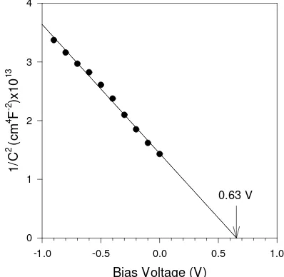
Figure 1 shows a plot of the inverse capacitance per unit area squared versus reverse bias at room temperature. The capacitance was measured at 1 MHz. The doping density calculated from this graph of n = 1.5x1018 cm-3 is in good agreement with the Hall data. This is the highest doping density reported for this material. From the C-V measurement data, the intercept voltage (Vi) was found to be 0.63 eV and the barrier height is calculated using Equation (10) to be 0.64 eV. This value is comparable to that found for Schottky diodes formed by Al deposition on Te-doped GaSb grown using different metalorganic sources (Poole et al., 1987; Roteli et al., 1997; Chen et al., 1996).
Bias Voltage (V)
3.3 Frequency Dependent C-V Measurements Frequency dependent C-V measurement were performed on the Schottky diode as a function of bias. Figure 2 shows typical response curves for a GaSb Schottky diode which indicate that the measured capacitance is dependent on the reverse bias voltage and frequency. The voltage and frequency dependence is due to the ideality factor of the Schottky barrier and due to a high series resistance (Sahin et al., 2005; Tararoglu and Altindal, 2006). At low frequency the measured capacitance is dominated by the depletion capacitance of the Al/n-GaSb Schottky diode which is bias-dependent and frequency-dependent. As the frequency is increased, the total diode capacitance is affected not only by the depletion capacitance but tunnelling which renders the device susceptible to stray inductances (Butcher et al., 1996). Because of these effects, the capacitance-bias dependence becomes less pronounced or disappears. The frequency dependence is weakened for high reverse voltages.
Bias Voltage (V)
-2 -1 0 1 2
Ca
pa
cita
nce (p
F)
0 100 200 300 400 500 600
100 kHz
500 kHz
1 MHz
2 MHz
Figure 2. The frequency dependence of the capacitance of the Al/n-GaSb Schottky diode at room temperature.
3.4 I-V Characteristics and Ideality Factor
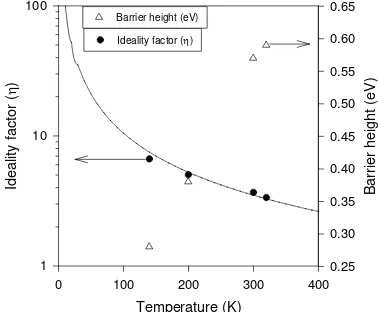
Low-temperature I-V measurements were conducted using a Cryostat system. A semilogarithmic plot of the I-V-T characteristics of a typical Al/n-GaSb diode over a temperature range of 140 - 320K and the linear part of the forward bias plot are shown in Figures 3 and 4 respectively. As shown in Figure 4, the saturation current density Jo (equation 1) is the intercept on the current axis at zero bias. Jo at 300 K was found to be 1.45x10⁻⁴ A/cm2. The room temperature value of barrier height
for the diode determined using equation (2) and was found to be 0.57 eV. The temperature dependence of the barrier height φB for the same sample is shown in Figure 5, where the barrier height of φB gradually decreases when the temperature is lowered. Temperature dependence, of η and φB, similar to that of Figure 5 indicates inhomogeneity at the metal-semiconductor interface (Tyagi, 1984; Saxana, 1969; Werner and Guttler 1991). Literature reports on the temperature dependence of φB are conflicting. Polyakov et al. (1992) showed that the φB for an Au Schottky barrier on GaSb was a decreasing function of temperature with temperature dependence identical to that of the band gap (Eg). Walters and Williams (1988) found that φB for an Au Schottky barrier on GaSb decreased more or less linearly with increasing temperature with a temperature coefficient of about -0.3x10⁻⁴ eV/K. This result is similar to the temperature dependence of φB of Figure 5 with a temperature coefficient of about -0.2x10⁻⁴ eV/K. On the other hand, Spicer et al. (1985) observe that the temperature dependence of φB for a Pd Schottky barrier on GaSb was much less than that of Eg. On theoretical grounds one would expect a temperature dependence of Eg to result in a temperature dependence of φB, because of a change in Eg-φo
where φ
0 is the neutral level for surface states. It is also expected that φB and χs, would change with temperature. The interpretation of the temperature dependence of φB is not clear.
The difference in barrier height as obtained from capacitance-voltage (C-V) and current-voltage (I-V) measurements on Al/n-GaSb Schottky barriers can be explained as follows: when comparing the values obtained for φB, 0.63 and 0.59 eV by C-V characteristics and I-V-T characteristics, respectively, the effects of an insulating layer or charges existing at the semiconductor-metal interface must be considered. Most Schottky diodes have a thin oxide or insulating layer at the metal-semiconductor junction unless all the processing is done in a vacuum. In the case of C-V measurements, an interface layer of several monolayers or so can significantly enlarge the value Vo determined at l/C2 = 0 and the measured barrier potential. Also, deep levels occurring in the GaSb band gap can affect capacitance measurements if they emit carriers to the conduction band at a rate comparable to the testing signal frequency of the capacitance meter.
The effective value of the Richardson coefficient that was used in this analysis, 5.4 A cm-2K-2, is very small compared to that determined theoretically based on the effective mass, 26 A cm-2K-2 using A*=(4πm* qk3/h3) (Tyagi, 1984). This would indicate the presence of a barrier through which the electrons must tunnel. The ideality factor
thin insulating layers on silicon, charged states which exist in equilibrium with the metal tend to hold the barrier height constant, thus the ideality factor η remains low. The present tests indicates that a very thin barrier exists at the junction through which the electrons must tunnel, but the potential drop across it remains fairly constant with applied voltage. The electric potential across this layer, or charges it contains, is a probable cause of the difference in the measured barrier heights by capacitance-voltage and current-voltage techniques.
The ideality factor (η) can be calculated from the linear part of the I-V curves as shown in Figure 4, according to equation (4). The diode shows a strong temperature dependence of ideality factor from approximately 3.6 at room temperature to as high as 6.7 at 140 K. There may be a small portion of the device nonideality attributable to generation-recombination currents due to deep levels in GaSb. Similar results have been reported by Chen et al., (1996). However tunnelling mechanisms probably provide a greater contribution to both the high device currents and device nonideality. Another possibility for the high leakage current is due to oxide layer on the GaSb epilayer as reported by Perotin et al., (1994) on Au/n-GaSb Schottky diode. Even though the removal of oxide layer during Schottky diode fabrication has been conducted, the exposure from the atmosphere was unavoided resulting a native oxide on n-GaSb surface. The oxide layer degraded the rectifying properties of metal contact deposited on the surface.
Voltage (V)
-2.0 -1.5 -1.0 -0.5 0.0 0.5 1.0 1.5 2.0
Curr
ent (A
)
10-7
10-6
10-5
10-4
T=320K T=300K T=200K T=140K
Figure 3. I-V-T characteristics of Al/n-GaSb Schottky diode.
Voltage (V)
0.00 0.04 0.08 0.12 0.16 0.20
Current d
ensity (A/cm
2 )
10-5
10-4
10-3
T = 320 K T = 300 K T = 200 K T = 140 K
Jo=1.45x10
-4 A/cm2
Figure 4. Plot of current density as a function forward bias in the temperature range 140 320 K.
Temperature (K)
0 100 200 300 400
Ideal
ity factor (
η
)
1 10 100
Ideality factor (η)
Barrie
r he
ight (e
V
)
0.25 0.30 0.35 0.40 0.45 0.50 0.55 0.60 0.65
Barrier height (eV)
Figure 5. Plot of ideality factor and barrier height versus temperature. Points are experimental data, the solid line is predicted by equation 13.
For materials with low doping level, nearly ideal diodes with ideality factors close to unity may be expected. In this case, η is insensitive to the temperature. A strong deviation of η from unity is evident for the Al/n-GaSb diodes prepared in this work because the starting material has a moderately high doping level. This is an indication that the tunnelling mechanism is involved in the current transport mechanism and the I-V relationship of equation 1 can then be rewritten in the form
⎥ ⎦ ⎤ ⎢
⎣ ⎡
⎟ ⎠ ⎞ ⎜ ⎝ ⎛− − ⎟⎟ ⎠ ⎞ ⎜⎜ ⎝ ⎛
kT qV
ηkT qV
J=Jsexp 1 exp , (12)
∗ =
=
m N kT
q D
ε ζ
ζ ζ η
2 with
coth h , (13)
where ћ is the reduced Planck constant, ε is the dielectric constant equal to 1.38 × 10⁻¹⁰ Fcm-1 for GaSb, m* is the electron effective mass equal to 0.38 × 1031 kg for GaSb and ND is the donor concentration. The ideality factor as a function of temperature predicted by equation (13) for the Al/n-GaSb Schottky diode is presented in Figure 5 (solid line). The data fit well for an assumed donor density of 2.1 × 1018 cm-3. This value is slightly higher than the value obtained from C-V measurements (see Figure 1). This is not surprising since the tunnelling current penetrates the tip of the barrier, which lies within a few monolayers of the interface where the local donor density may be higher than that in the bulk.
3.5 Sample Annealing
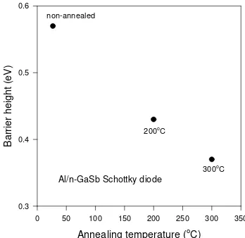
The electrical properties of Al/n-GaSb Schottky barriers were compared following annealing under various conditions. The effect of annealing is clearly observed. The room temperature I-V characteristics of an Al/n-GaSb Schottky diode following different annealing temperature treatments is shown in Figure 6. At room temperature, the diode shows a relatively good forward and reverse characteristics. The I-V characteristic becomes more ohmic with higher annealing temperatures and higher current currents are evident. The barrier height measured from the I-V characteristics, as a function of the annealing temperature, for an Al/n-GaSb diode is shown in Figure 7. The barrier height decreased from 0.57 eV to 0.35 eV for the sample annealed at 300oC for 1 minute. In general, the barrier height was found to decrease with increasing annealing time. The barrier lowering may be partly due to an increase in doping concentration at the metal-semiconductor interface caused by metal in diffusion from the metal barrier. This is confirmed by C-V measurements. Finally, the Schottky diodes become completely ohmic as the annealing temperature is raised to 400oC for 1 minute due to interaction of metal and semiconductor (Su et al., 1990).
Voltage (V)
-2.5 -2.0 -1.5 -1.0 -0.5 0.0 0.5 1.0 1.5
C
u
rrent (A)
-0.0003 -0.0002 -0.0001 0.0000 0.0001 0.0002 0.0003
non-annealed
200o C 300oC
400o C
Figure 6. I-V characteristics of the Al/n-GaSb Schottky diode at different annealing temperatures.
Annealing temperature (oC)
0 50 100 150 200 250 300 350
Barri
er hei
g
ht (eV)
0.3 0.4 0.5 0.6
non-annealed
200o C
300o C Al/n-GaSb Schottky diode
Figure 7. The barrier height as a function of annealing temperature (annealing time at 1 minute). 4. Conclusions
measurements. The Schottky diode capacitance is dependent on the reverse bias voltage and frequency. As the frequency is increased, the total diode capacitance is affected not only by the depletion capacitance but tunnelling which renders the device susceptible to stray inductances. After annealing, the barrier height decreased from 0.57 eV to 0.35 eV for an Al/n-GaSb sample annealed at 300oC for 1 minute. The barrier lowering may be partly due to an increase in doping concentration at the metal-semiconductor interface.
Acknowledgment
The authors would like to acknowledge the assistance of Macquarie University Sydney- Australia for access provided to the clean-room facility and the I-V and C-V measurement instruments.
References
Ahmetoglu M., I. Andreev, E. Kunitsyna, M. Mikhailova, and Y. Yakovlev, 2007, Electrical properties of isotype
n-GaSb/n-GaInAsSb/n-GaAlAsSb type-II heterojunctions, Semiconductors 41,
150-154.
Ait Kaci H., D. Boukredimi, and M. Mebarki, 2001, Current–Voltage Characteristic and Schottky Barrier Height of the GaAlAsSb(p)/GaSb(n+) Heterostructure, Physica Status Solidi (a), 183, 345-351.
Butcher K.S.A, T.L. Tansley and D. Alexiev, 1996, An instrumental solution to the phenomenon of negative capacitances in semiconductors, Solid-State Electron. 39, 333-336.
Chen J.F., N.C. Chen, and H.S. Liu, 1996, Deep levels, electrical and optical characteristics in SnTe-doped GaSb Schottky diodes, J. Electronic Materials, 25, 1790-1800. Crowel C.R. and S.M. Sze, 1966, Current Transport
in Metal-Semiconductor Barrier, Solid-State Electron. 9, 1035-1048.
Dimoulas, A., P. Tsipas, A. Sotiropoulos, and E. K. Evangelou, 2006, Fermi-level pinning and charge neutrality level in germanium, Appl. Phys. Lett. 89, 252110-3.
Li, B.K., M. J. Wang, K. J. Chen, J. N. Wang, 2010, Electroluminescence from a forward biased Ni/Au–AlGaN/GaN Schottky diode: evidence of Fermi level de-pinning at Ni/AlGaN interface, Phys. Stat. Solid. C 7, 1961–1963.
Liu Z.Y., D. A. Saulys, and T. F. Kuecha, 2004, Improved characteristics for Au/n-GaSb Schottky contacts through the use of a nonaqueous sulfide-based passivation, Appl. Phys. Lett. 85, 4391-4393.
Mead C.A., 1966, Metal-semiconductor surface barriers, Solid-State Electron. 9, 1023-1033.
Milnes A.G. and A.Y. Polyakov, 1993, Review GaSb device related properties, Solid State Electron. 36, 803-818.
Mott N.F.,1938, Proc. Comb. Philos. Soc., 34, 568-572.
Padovani F.A. and R. Stratton, 1966, Field and Thermionic-Field Emission in Schottky Barriers, Solid-State. Electronics, 9, 695-707.
Perotin M., P. Coudray, L. Gouskov, H. Luquet, J.J. Bonnet, L. Soonckindt, and B. Lambert, 1994, In situ Schottky contacts to epitaxially grown gallium antimonide, J. Electron. Mater. 23, 7-12.
Polyakov A.Y., M. Stam, A.G. Milnes, and T.E. Schlesinger, 1992, Mater. Sci. Eng. B12, 337-341.
Poole I., M.E. Lee, M.Missous, and K.E. Singer, 1987, In situ Schottky contacts to molecular-beam epitaxy, J. Appl. Phys. 62, 3988-3990.
Rhoderick E.H. and R.H. Williams, 1988, Metal-Semiconductor Contacts, 2nd, Clarendon Press, Oxford.
Rotelli B., L. Tarricone, E. Gombia, R. Mosca, and M. Perotin, 1997, Photoelectric properties of GaSb Schottky diodes , J. Appl. Phys. 81, 1813-1819.
Sahin, B., H. Çetin and E. Ayyildiz, 2005, The effect of series resistance on capacitance–voltage characteristics of Schottky barrier diodes, Solid State Communic. 135, 490-495.
Saxana A.N., 1969, Forward current-voltage characteristics on n-type silicon, Surface Science 13, 151-171.
Schottky W., Halbleitertheorie der Sperrschicht, 1938, Naturwissenschaften, 26, 843-844. Su Y.K., N.Y. Li, F.S. Juang, 1990, The effect of
annealing temperature on electrical properties of Pd/n-GaSb Schottky contacts, and S.C. Wu, J. Appl. Phys. 68, 646 - 648. Sze S.M., 1981, Physics of Semiconductor Devices ,
John Wiley & Son, 259.
Tararoglu, A., S. Altindal, 2006, Characterization of current–voltage (I–V) and capacitance– voltage–frequency (C–V–f) features of Al/SiO2/p-Si (MIS) Schottky diodes, Microelect. Engineering , 83, 582-588. Tyagi M.S., 1984, Metal Semiconductor Schottky
Barrier Junctions and their Application (Edited by Sharama B.L) p. 48, Plenum, New York p. 48.
Walters S.A. and R.H. Williams, 1988, Metals on cleaved gallium antimonide: Schottky barriers and interface reactions ,J. Vac. Sci. Technol. B6, 1421-1426.