A Novel Configuration Circuit Architecture to Speedup Reconfiguration and
Relocation for Partially Reconfigurable Devices
Thomas Marconi, Jae Young Hur, Koen Bertels, Georgi Gaydadjiev
Computer Engineering Laboratory, EEMCS
Delft University of Technology
{
thomas,j.y.hur,koen,georgi
}
@ce.et.tudelft.nl
Abstract—Long reconfiguration times form a major bottleneck
in dynamic reconfigurable systems. Many approaches have been proposed to address this problem. However, improvements in the configuration circuit that introduces this overhead are usually not considered. The high reconfiguration times are due to the large amount of configuration bits sent through a constrained data path. In order to alleviate this, we propose a novel FPGA configuration circuit architecture to speedup bitstream (re)configuration and relocation. Experimental results using the MCNC benchmark set indicate that our proposal reconfigures 4 times faster and relocates 19.8 times more efficient compared to the state of the art approaches. This is achieved by transporting only the data required for the configuration in flight and by avoiding external communication while relocating. Moreover, the configuration bitstream sizes of the evaluated benchmarks are reduced by 65 % on average. In addition, our proposal introduces negligible hardware and communication protocol overheads.
I. INTRODUCTION
Modern FPGA devices support partial reconfiguration that allows runtime changes of the system functionality. Various benefits can be achieved by exploiting this property, e.g., reduced power consumption, minimized hardware cost, im-proved system performance, and more [5]. However, there is a problem related to the reconfiguration time penalties that one has to address in order to fully benefit from the above. This problem is even more restrictive for systems where reconfigurations occurs frequently. This high reconfiguration time overheads can eclipse the overall benefits of FPGA based systems. The major bottleneck is introduced by the configuration circuit since it needs to transport large amounts of configuration data (bitstreams) using a limited configuration data path. FPGAs being fine-grained reconfigurable devices, in general require a large amount of configuration bits. In addition, the overall FPGA sizes are also increasing very fast. As a result, the bitstream sizes are growing. Furthermore, to cope with FPGA area fragmentation during runtime, it is needed to efficiently reorganize the positions of the active hardware cores. Such reorganizing process requires fast bit-stream relocations.
To solve the above problems, in this paper we propose a novel FPGA configuration circuit architecture to speedup bitstream reconfiguration and relocation. The proposal is eval-uated using the Microelectronic Center of North Carolina (MCNC) benchmark circuits [1]. Each benchmark circuit is translated to an equivalent VHDL code before synthesis, mapping, place, and route onto a Xilinx Virtex-4 FPGA. We targeted XC4VLX200-10FF1513 device using Xilinx ISE
8.2.01i PR 5 tools. Based on the MCNC circuits, our proposal is evaluated against the conventional Virtex-4 reconfiguration process. In terms of relocation times, we compare against a system that modifies the reconfiguration data before sending it to the FPGA configuration circuit during relocation as proposed in [24]-[28]. We also investigate the bitstream size reduction and the hardware overhead of our proposal. The required hardware to implement our architecture is described in VHDL and verified using ModelSim simulation. The ver-ified hardware is synthesized in ASIC with 90 nm CMOS technology using Cadence Encounter tools to obtain the hard-ware overhead numbers. Considering the fact that no data is available about the exact size of the Xilinx configuration circuit, we compare our proposal against the overall Virtex-4 die size obtained from [2].
The main contributions of this paper are:
• a novel FPGA configuration circuit architecture to
sup-port fast reconfiguration and relocation with negligible hardware overhead (0.009 % of the overal Virtex-4 area);
• significant improvements in reconfiguration and
reloca-tion times of 4x and 19.8x respectively;
• reduction of reconfiguration bitstream sizes by 65% on
average.
The remainder of this paper is organized as follows. In Section II, we present the problems related to dynamically reconfigurable computing systems and the most relevant state of the art solutions. The proposed architecture aimed to solve the problem is presented in Section III. In Section IV, we evaluate our proposal by comparing it with the contemporary architecture. Finally, in Section V, we summarize the paper.
II. RELATED WORK
FPGAs is another way to deal with long reconfiguration times as proposed by [9] and [10]. However, n-context FPGAs need n times more SRAM memory for saving configuration data. Creating multi-channel configuration circuits to recon-figure FPGAs can also be used for shortening reconfiguration time [4]. Bitstream compression has been also proposed to speedup reconfiguration if the bottleneck is in transferring data from memory to controller to drive configuration circuit (e.g. [11],[12]). However, the maximal configuration speed is still limited by the maximum speed of configuration circuit [12]. Maximizing module overlap to reduce reconfiguration time is presented in [13]. Adding unused configuration frames into cost function during routing can minimize the number of used frames [14]. As a result, the bitstream size is decreased, thereby leading to short reconfiguration times. Combining module reuse and configuration prefetching techniques to minimize reconfiguration time is presented in [15]. Reusing previously communication infrastructure to minimize recon-figuration overhead for task communications is proposed in [16]. To reduce reconfiguration overhead, maximizing com-mon components between two successive configurations is presented in [17]. Combining configuration prefetching and anti-fragmentation techniques to reduce reconfiguration time is proposed in [18]. To minimize reconfiguration overhead in [19], the LUT input orders are permuted such a way that the changing memory bits are located into some common frames. Placing the logic elements into the least slice columns as possible is another solution to reduce reconfiguration overhead [20]. Minimizing the number of reconfigurable regions to be reconfigured during runtime is another way to reduce reconfig-uration time [21]. Loop transformations to reduce the number of needed reconfigurations is presented in [22]. Increasing similarity of logic blocks configuration for subsequent circuits can be used to reduce reconfiguration overhead [23].
All above solutions have a common characteristic that they do not directly target the configuration circuit architecture (the major bottleneck of this high reconfiguration cost). In this paper, we propose a new FPGA configuration circuit architecture to tackle this major bottleneck.
III. PROPOSEDARCHITECTURE
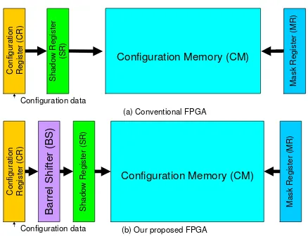
In [29], Young et al. patented an architecture for FPGA partially reconfiguration referred as the conventional FPGA/architecture in this paper. The main difference between our proposal (Figure 1(b)) and the conventional architecture (Figure 1(a)) is the Barrel Shifter (BS). This additional com-ponent is the key idea of our architecture that allows us to overcome the limitation of the conventional architecture by avoiding shifting and transferring of unnecessary configuration bits.
In the conventional FPGA as presented in [29], a frame of configuration data is loaded serially into a shift register (Configuration Register (CR)) at times t=t1 to t=t5 as illus-trated in Figure 2(a). After the entire frame is loaded into CR, it is temporarily transferred to a Shadow Register (SR) (Figure 2(a) at t=t6) so that the CR is free to begin receiving
Configuration Memory (CM)
Configuration Register (CR)
Shadow Register
(SR)
Mask Register (MR)
Configuration data
Configuration Memory (CM)
Configuration Register (CR)
Shadow Register (SR) Mask Register (MR)
Configuration data
Barrel Shifter (BS)
(a) Conventional FPGA
(b) Our proposed FPGA
Fig. 1. Architecture of the conventional FPGA versus our proposed FPGA
t=t1 t=t2 t=t3 t=t4 t=t5
t=t6 t=t7
t=t1 t=t2 t=t3 t=t4
(a) Conventional FPGA
(b) Our proposed FPGA
Fig. 2. Reconfiguration steps of the conventional FPGA versus our proposed FPGA
the next frame of data. An address line is used to transfer the data from the shadow register via the data lines into the selected Configuration Memory (CM) cells as illustrated in Figure 2(a) at t=t7. The Mask Register (MR) selects which memory cells receive the specific configuration data values and which memory cells do not, thereby defining a partial reconfiguration zone as shown in the same figure. In this simple example, we can see that although the reconfiguration circuit of the conventional FPGA can partially reconfigure the selected FPGA area, the needed reconfiguration time is still high. This high reconfiguration time overhead is caused by the shifting of unneeded configuration data (dummy data) along with the needed one.
Frame Height (FH)
CR BS SR
Frame Height Displacement (FHD)
Fig. 3. Mechanism of our proposed architecture
CR as illustrated in Figure 1(b) and Figure 2(b). BS is used to facilitate in transferring the needed configuration data from CR to a specific position in SR. In the proposed FPGA, only the needed configuration data are loaded into CR as shown in Figure 2(b) at t=t1 to t2. After a part of the entire frame (the needed configuration data) is shifted into CR, the configuration data are temporarily transferred to SR through BS (Figure 2(b) at t=t3). Finally, this configuration data are transferred to selected partial reconfiguration zone defined by MR as illustrated in Figure 2(b) at t=t4. Based on this simple example, we can see that our proposed architecture only needs 4 steps instead of 7 steps present in the conventional FPGA in reconfiguring the same partial reconfiguration area.
To support the mechanism of our proposed architecture in shifting configuration data partially from CR register to a specific position in SR register through Barrel Shifter (Figure 3), the proposed architecture needs the additional hardware enclosed between the dashed lines in Figure 4. The hardware needs to know how much configuration data should be shifted (Frame Height (FH)) and how far the configuration data must be shifted (Frame Height Displacement(FHD)). In order to control FH, we add Frame Height Counter (FHC), Frame Height Register (FHR) and Comparator. This simple structure can control the frame height by writing a specific FH value to FHR during the execution of a set frame height command (FHR initialization). The value of FHC is increased every time the configuration data are shifted into the CR register. When the FHC reaches the same value as FHR, the stop signal from this circuit prevents CR shifting configuration data further. The frame height displacement is controlled by setting the Frame Height Displacement Register (FHDR) using a set height displacement command. This way, we can place the configuration data to the right position into SR in order to partially reconfigure the FPGA with minimal configuration time overhead.
Instead of including unnecessary dummy data in
conven-Comparator
Frame Height Register (FHR)
Frame Height Counter (FHC)
Stop Configuration
Register (CR)
Barrel Shifter (BS)
Frame Height Displacement Register (FHDR)
Frame Height Displacement (FHD)
Shadow Register (SR)
Fig. 4. Hardware overhead for supporting fast reconfiguration
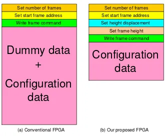
Set number of frames Set start frame address Write frame command
Set number of frames Set start frame address Set height displacement
Dummy data
+
Configuration
data
(a) Conventional FPGA (b) Our proposed FPGA Set frame height Write frame command
Configuration
data
Fig. 5. Bitstream for reconfiguration
tional bitstream for reconfiguration (Figure 5(a)), our proposed architecture only includes the required reconfiguration data in the bitstream (Figure 5(b)). This feature reduces the configu-ration bitstream size, consequently it decreases the required memory/hardware for storing the bitstream. In addition to setting the number of frames and the start frame address, before we can write configuration data, we have to set two additional parameters: frame height displacement and frame height using the corresponding set height displacement (to initialize FHDR) and set frame height (to initialize FHR) commands.
Although our proposal can be generally used for any partially reconfigurable FPGAs, we use Virtex-4 [4] as our case study. There are 22 frames per Virtex-4 CLB column and each frame contains 41 words = 41x32 = 1312 bits. Therefore one column CLB needs 22x1312 = 28864 bits. Since one CLB column of Virtex-4 FPGA consists of 16 CLBs,
one CLB contains 28864/16 = 1804 bits. Based on these
RCBSSconv = (3×32) + (28864× ⌈h/16⌉ ×w). The factor
(3x32) is for set number of frames (32 bits), set start frame ad-dress (32 bits), and write frame command (32 bits) as shown in Figure 5(a). Since the atomic reconfiguration unit in Virtex-4
is a frame, the⌈h/16⌉is used in this equation. Thehandware
the core height and width in number of CLBs. Since the atomic reconfiguration unit in our proposal is a CLB, reconfiguration bitstream size in number of bits for our proposed architecture
is estimated as RCBSSour = (5×32) + (1804×h×w).
The factor (5x32) is for set number of frames (32 bits), set start frame address (32 bits), set height displacement (32 bits), set frame height (32 bits), and write frame command (32 bits) as shown in Figure 5(b). Since Virtex-4 has 32-bit configuration data path, it can transfer 32 32-bits of data per clock cycle. As a result, the reconfiguration time in number of clock cycles for the conventional architecture is
RCTconv = RCBSSconv/32. Using the same assumptions,
the reconfiguration time in number of clock cycles for our
architecture isRCTour =RCBSSour/32.
In this paper, we also propose a new specialized con-figuration command to support core relocations. Instead of modifying target address and resending the modified recon-figuration data in order to do relocation as proposed by several authors (e.g. [24]-[28]) using the conventional FPGA (Figure 6(a)), using the proposed relocation command pro-vides with the opportunity to perform relocation without resending the reconfiguration data since the reconfiguration data are already in configuration memory (Figure 6(b)). To do relocation efficiently, our proposed relocation command copies the relocatable core from configuration memory to the shadow register and then directly writes it back to the target location per frame basis as illustrated in Figure 6(b). This new mechanism of relocation makes core relocation faster since we do not need to resend configuration data outside of the FPGA device. This will significantly reduce the configuration path utilization during relocation. Three additional registers are needed to support fast relocation: source start frame address register (SSFAR), target height displacement register (THDR), and source height displacement register (SHDR). To facilitate fast relocation, we need to set additional parameters:
• source start frame address using a set source start frame
address command;
• target height displacement using a set target height
dis-placement command;
• source height displacement using a set source height
displacement command;
• frame height using a set frame height command.
Since the read back capability is already supported by the Virtex-4 devices, no extra hardware is needed to read back configuration memory.
Based on Virtex-4 FPGA information and Figure 7, the relocation bitstream size in number of bits for the conventional
FPGA can be estimated asRLBSSconv= (3×32)+(28864×
⌈h/16⌉ × w) due to the need to resending configuration
bitstream. The factor (3x32) is for set number of frames (32
Shadow Register
(SR)
Configuration Reg
ister (CR)
Configuration Memory (CM)
Resending configuration data Target start frame address Number of frames
Without resending configuration
data Target start frame address
Number of frames
Relocatio n
Barrel Shifter (BS)
Source start frame address
(b) Our proposed FPGA
Fig. 6. Core relocation
Set number of frames Set target start frame address
Write frame command
Set number of frames Set target start frame address Set source start frame address Set target height displacement Set source height displacement
Relocation command
(a) Conventional FPGA (b) Our proposed FPGA Set frame height
Dummy data
+
Configuration
data
Fig. 7. Bitstream for core relocation
bits), set target start frame address (32 bits), and write frame command (32 bits) as shown in Figure 7(a). Since our archi-tecture does not need to resend configuration bitstream during relocation, the relocation bitstream size in number of bits for
the our FPGA is constant (RLBSSour= 7×32). The factor
(7x32) is for set six parameters (number of frames, target start frame address, source start frame address, target height displacement, source height displacement, frame height), and also for the relocation command as shown in Figure 7(b). Using 32-bit configuration data path, the relocation time in number of clock cycles for the conventional architecture is
RLTconv = RLBSSconv/32. Since our proposed relocation
command needs to read configuration memory (assume one clock cycle) and write configuration memory (assume another clock cycle) per frame for relocation and each CLB column has 22 frames, the reconfiguration time in number of clock
cycles for our architecture is RLTour = (RLBSSour/32) +
TABLE I
SPEEDUP(TIMES)AND BITSTREAM SIZE(BSS)REDUCTION(%)COMPARED TO THE CONVENTIONALFPGA
Circuit name Circuit function Slices Reconfiguration Relocation
RCTconv RCTour Speedup BSSconv BSSour Reduction(%) RLTconv RLTour Speedup
bigkey Key Encription 683 12631 11055 1.14 404192 353744 12.48 12631 623 20.27
clma Bus Interface 1560 36083 22555 1.6 1154656 721760 37.49 36083 1767 20.42
dsip Encription Circuit 475 9925 6827 1.45 317600 218444 31.22 9925 491 20.21
mm30a Minmax Circuit 196 6317 2768 2.28 202144 88556 56.19 6317 315 20.05
mm4a Minmax Circuit 34 2709 513 5.28 86688 16396 81.09 2709 139 19.49
mm9a Minmax Circuit 72 4513 1415 3.19 144416 45260 68.66 4513 227 19.88
mm9b Minmax Circuit 114 5415 2035 2.66 173280 65104 62.43 5415 271 19.98
mult16a Multiplier 41 3611 907 3.98 115552 29024 74.88 3611 183 19.73
mult16b Multiplier 16 1807 231 7.82 57824 7376 87.24 1807 95 19.02
mult32a Multiplier 115 5415 2035 2.66 173280 65104 62.43 5415 271 19.98
sbc Snooping Bus Controller 150 6317 2768 2.28 202144 88556 56.19 6317 315 20.05
s27 Logic 4 905 62 14.6 28960 1964 93.22 905 51 17.75
s208.1 Digital Fractional Multiplier 14 1807 231 7.82 57824 7376 87.24 1807 95 19.02
s298 PLD 340 9023 5643 1.6 288736 180560 37.47 9023 447 20.19
s344 4-bit Multiplier 22 2709 513 5.28 86688 16396 81.09 2709 139 19.49
s349 4-bit Multiplier 22 2709 513 5.28 86688 16396 81.09 2709 139 19.49
s382 Traffic Light Controller 27 2709 513 5.28 86688 16396 81.09 2709 139 19.49
s386 Controller 26 2709 513 5.28 86688 16396 81.09 2709 139 19.49
s400 Traffic Light Controller 26 2709 513 5.28 86688 16396 81.09 2709 139 19.49
s420.1 Digital Fractional Multiplier 28 2709 513 5.28 86688 16396 81.09 2709 139 19.49
s444 Traffic Light Controller 31 2709 513 5.28 86688 16396 81.09 2709 139 19.49
s510 Controller 53 3611 907 3.98 115552 29024 74.88 3611 183 19.73
s526n Traffic Light Controller 24 2709 513 5.28 86688 16396 81.09 2709 139 19.49
s526 Traffic Light Controller 24 2709 513 5.28 86688 16396 81.09 2709 139 19.49
s641 PLD 35 2709 513 5.28 86688 16396 81.09 2709 139 19.49
s713 PLD 43 3611 907 3.98 115552 29024 74.88 3611 183 19.73
s820 PLD 68 4513 1415 3.19 144416 45260 68.66 4513 227 19.88
s832 PLD 79 4513 1415 3.19 144416 45260 68.66 4513 227 19.88
s828.1 Digital Fractional Multiplier 60 3611 907 3.98 115552 29024 74.88 3611 183 19.73
s1196 Logic 112 5415 2035 2.66 173280 65104 62.43 5415 271 19.98
s1423 Logic 156 6317 2768 2.28 202144 88556 56.19 6317 315 20.05
s1488 Controller 138 5415 2035 2.66 173280 65104 62.43 5415 271 19.98
s1494 Controller 143 5415 2035 2.66 173280 65104 62.43 5415 271 19.98
s5378 Logic 276 8121 4572 1.78 259872 146284 43.71 8121 403 20.15
s38417 Logic 2359 45103 35240 1.28 1443296 1127660 21.87 45103 2207 20.44
s9234.1 Logic 193 6317 2768 2.28 202144 88556 56.19 6317 315 20.05
s38584.1 Logic 2127 43299 32477 1.33 1385568 1039264 24.99 43299 2119 20.43
IV. EVALUATION
To evaluate our proposed architecture, we used the Micro-electronic Center of North Carolina (MCNC) benchmark set from [1]. Each benchmark circuit was translated to an equiv-alent VHDL code before it was synthesized, mapped, placed, and routed onto a Xilinx Virtex-4 FPGA with part number XC4VLX200-10FF1513 using Xilinx ISE 8.2.01i PR 5 tools. Using these FPGA-implemented MCNC circuits, the proposal was evaluated against the conventional one (Virtex-4 in this case study) in terms of reconfiguration and relocation times and the bitstream sizes.
We assume that the frame utilization (the ratio between number of required bits in a frame and total number of bits in a frame) is equal to the logic utilization. It is well-known that the wire utilization is much lower than the logic utilization. Therefore we consider that the assumption is conservative in that actual frame utilization is significantly lower than the logic utilization. Since a circuit with a square shape performs the best in terms of area and speed as shown in [30], each benchmark circuit was implemented in a free square-shaped-area of the FPGA.
Table I shows the speedup (times) and bitstream size (BSS) reduction (%) of our proposed architecture compared to the conventional architecture both for reconfiguration and
reloca-tion. From this table, we can see that the proposed architecture has on average 4 times shorter reconfiguration times compared to the conventional approaches. The reconfiguration time re-duction (speedup) can improve up to 14.6 times for a small circuit (s27) since the amount of dummy data increases when the circuit is smaller. In this case, the conventional architecture is very slow in reconfiguring the FPGA, while our proposal becomes very fast since we do not need to feed dummy data. Moreover, the reconfiguration bitstream size is reduced up to 93.22 % compared to the conventional FPGA since we do not include dummy data in our bitstream file.
Table I also shows that our proposal relocates cores faster than the conventional architecture. On average, our proposal can do relocation 19.8 times faster than the conventional FPGA by avoiding resending configuration data during relocation using the proposed specialized relocation command.
TABLE II AREA OVERHEAD
Modules Area(µm2)
Barrel Shifter (BS) 61881
Comparator 450
Frame Height Displacement Register(FHDR) 1092 Frame Height Counter (FHC) 1650 Frame Height Register (FHR) 1092 Source Start Frame Address Register (SSFAR) 1092 Target Height Displacement Register (THDR) 1092 Source Height Displacement Register (SHDR) 1092
Total Area Overhead 69441
To compare our proposal against Virtex-4 in terms of area, the estimated die size of Virtex-4 FPGA was obtained from
[2]. Considering the area(=735mm2) of the targeted Virtex-4
FPGA device (Estimated die size from [2]), the area overhead of the architecture is very small. The total area overhead is only 0.009 % of the Virtex-4 area.
V. CONCLUSIONS
In this paper, we have introduced a novel configuration circuit architecture for partially reconfigurable FPGAs, that supports faster bitstream reconfiguration and relocation. More precisely, our proposal is 4x faster during reconfiguration of the MCNC benchmark circuits compared to Xilinx Virtex-4. In addition, the area overhead of the proposed architecture is only 0.009 % of the overall Virtex-4 area. For fast 2D relocation, we proposed a new specialized command in the configuration protocol. With this new command, hardware core relocation is facilitated without resending configuration data externally. Our experimental results show that our architecture is 19.8x faster during relocation compared to the current state the art (Virtex-4). Moreover, the bitstream sizes of the investigated MCNC benchmarks are reduced by 65 % on average when our approach is applied.
ACKNOWLEDGMENT
This work is supported by the hArtes project (IST-035143) and the STW ARTEMISIA project (number LES.6389).
REFERENCES
[1] S. Yang, ”Logic Synthesis and Optimization Benchmarks User Guide Version 3.0,” Technical Report, Microelectronic Center of North Car-olina (MCNC), 1991.
[2] http://www.fpga-faq.org/
[3] Xilinx, Inc, ”Virtex-II Platform FPGA User Guide,” Xilinx user guide UG002, 2007.
[4] Xilinx, Inc, ”Virtex-4 FPGA Configuration User Guide,” Xilinx user guide UG071, 2008.
[5] C. Kao, ”Benefits of Partial Reconfiguration,” Xilinx Xcell Journal, 2005.
[6] S. Hauck, ”Configuration Prefetch for Single Context Reconfigurable Coprocessors,” Proceedings of International Symposium on Field-Programmable Gate Arrays, pp. 65-74, 1998.
[7] H. Schmit, ”Incremental reconfiguration for pipelined applications,” Proceedings of Symposium on FPGAs for Custom Computing Machines, pp. 47-55, 1997.
[8] Z. Li, K. Compton, S. Hauck, ”Configuration Caching Techniques for FPGA,” Proceedings of Symposium on FPGA for Custom Computing Machines, 2000.
[9] S. Trimberger, ”A Time-Multiplexed FPGA,” Proceedings of Sympo-sium on FPGA-Based Custom Computing Machines, pp. 22-28, 1997.
[10] A. DeHon, ”Dynamically Programmable Gate Arrays: A step toward in-creased computational density,” Proceedings of the Canadian Workshop on Field-Programmable Devices, pp. 47-54, 1996.
[11] R. A. Stefan, S. D. Cotofana, ”Bitstream Compression Techniques for Virtex 4 FPGAs,” Proceedings of International Conference on Field Pro-grammable Logic and Applications, pp. 323-328, Heidelberg, Germany, September 2008.
[12] D. Koch, C. Beckhoff, J. Teich, ”Hardware Decompression Techniques for FPGA-Based Embedded Systems,” ACM Transactions on Reconfig-urable Technology and Systems, Vol. 2, Issue 2, June 2009.
[13] A. Jara-Berrocal and A. Gordon-Ross, ”Runtime Temporal Partitioning Assembly to Reduce FPGA Reconfiguration Time,” Proceedings of International Conference on Reconfigurable Computing and FPGAs, pp.374-379, December 2009.
[14] J. T. Young, J. V. Lindholm, I. L. McEwen, ”Routing with Frame Awareness to Minimize Device Programming Time and Test Cost,” US Patent No. 7149997 B1, 2006.
[15] J. Resano, D. Mozos, D. Verkest, S. Vernalde, and F. Catthoor, ”Run-time Minimization of Reconfiguration Overhead in Dynamically Recon-figurable Systems,” Proceedings of International Conference on Field-Programmable Logic and Applications, pp. 585-594, 2003.
[16] S. Koh, O. Diessel, ”Module Graph Merging and Placement to Reduce Reconfiguration Overheads in Paged FPGA Devices,” Proceedings of In-ternational Conference on Field-Programmable Logic and Applications, pp. 293-298, 2007.
[17] N. Shirazi , W. Luk , P. Y. K. Cheung, ”Automating Production of Run-Time Reconfigurable Designs,” Proceedings of Symposium on FPGAs for Custom Computing Machines, pp. 147-156, April 15-17, 1998. [18] F. Redaelli, M.D. Santambrogio and D. Sciuto , ”Task Scheduling with
Configuration Prefetching and Anti-Fragmentation Techniques on Dy-namically Reconfigurable Systems,” Proceedings of Design, Automation and Test in Europe, pp. 519-522, March 2008.
[19] K. P. Raghuraman, H. Wang, S. Tragoudas, ”A Novel Approach to Minimizing Reconfiguration Cost for LUT-Based FPGAs,” Proceedings of International Conference on VLSI Design, pp. 673-676, 2005. [20] H. Tan, R. F. DeMara, ”A Physical Resource Management Approach
to Minimizing FPGA Partial Reconfiguration Overhead,” Proceedings of International Conference on Reconfigurable Computing and FPGAs, pp. 86-90, 2006.
[21] V. Rana, S. Murali, D. Atienza, M. Santambrogio, L. Benini, D. Sciuto, ”Minimization of the Reconfiguration Latency for the Mapping of Applications on FPGA-based Systems,” Proceedings of International Conference on Hardware/software Codesign and System Synthesis, pp. 325-334, 2009.
[22] T. Degryse, K. Bruneel, H. Devos, D. Stroobandt, ”Loop Transfor-mations to Reduce the Dynamic FPGA Reconfiguration Overhead,” Proceedings of International Conference on Reconfigurable Computing and FPGAs, pp. 133-138, 2008.
[23] W. Chen, Y. Wang, X. Wang, C. Peng, ”A New Placement Approach to Minimizing FPGA Reconfiguration Data,” Proceedings of International Conference on Embedded Software and Systems, pp. 169-174, 2008. [24] T. Becker, W. Luk, P.Y.K. Cheung, ”Enhancing Relocatability of Partial
Bitstreams for Run-Time Reconfiguration,” Proceedings of Symposium on Field-Programmable Custom Computing Machines, pp. 35-44, 2007. [25] H. Kalte, G. Lee, M. Porrmann, U. R¨uckert, ”REPLICA: A Bitstream Manipulation Filter for Module Relocation in Partial Reconfigurable Systems,” Proceedings of International Parallel and Distributed Process-ing Symposium, pp.151b, 2005.
[26] H. Kalte and M. Porrmann, ”REPLICA2Pro: Task Relocation by Bit-stream Manipulation in Virtex-II/Pro FPGAs,” Proceedings of Interna-tional Conference on Computing Frontiers, pp. 403-412, 2006. [27] Edson L. Horta and John W. Lockwood, ”Automated Method to
Generate Bitstream Intellectual Property Cores for Virtex FPGAs,” Proceedings of International Conference on Field-Programmable Logic and Applications, pp. 975-979, 2004.
[28] Y. E. Krasteva, A. B. Jimeno, E. Torre, T. Riesgo, ”Straight Method for Reallocation of Complex Cores by Dynamic Reconfiguration in Virtex II FPGAs,” Proceedings of International Workshop on Rapid System Prototyping, pp. 77-83, 2005.
[29] S. P. Young, T. J. Bauer, ”Architecture and Method for Partially Reconfiguring an FPGA,” US Patent No. 6526557 B1, 2003. [30] P. Hallschmid, S. J. E. Wilton, ”Detailed Routing Architectures for