Effect of plasma surface pre-treatment on plastic substrate for ZnO TFT
Feri Adriyanto
1, Po-Wen Sze
2and Yeong-Her Wang
11Institute of Microelectronics, Department of Electrical Engineering, National Cheng Kung University,
Tainan, 701 Taiwan
Tel: 06-2757575-62400-252/250/248, Fax: 886-6-2080598, E-mail: [email protected]
2Department of Electrical Engineering, Kao-Yuan University of Technology,
Lu-Chu, Kaoshiung, 821 Taiwan
Abstract
Controlling the surface morphologies of ZnO nanostructures is a critical issue for the fabrication of electronic and photonic devices. This study reports the electrical properties of the ZnO nanostructure grown on the plasma surface pre-treated plastic substrates. The ZnO films were grown by using solution method with zinc nitrate hexahydrate Zn(NO3)2•6H2O and hexamethylenetetramine
C12H6N4.as the main solution under various deposition
conditions. The films with plasma surface pre-treatment has stronger (100) peak intensity than that without plasma surface pre-treatment. Also, very uniform grain size of the ZnO nanostructures can be seen. The fabricated enhancement mode ZnO thin film transistors (TFTs) exhibiting good transistor behavior with the drain saturation current of 38.1 µA at VGS = 35 V can be achieved.
Keywords: ZnO nanostructure, plastic substrate, solution method, plasma, surface pre-treatment, TFT.
Introduction
Recently, ZnO semiconductors have been found useful in thin films transistors (TFTs) applications due to its wide band gap of 3.3 eV and a large exciton binding energy of 60 meV at room temperature [1]. So far, most ZnO layer for TFTs have been deposited under high growth temperature, so there is only limited cost production. Solution based processes for ZnO could be low cost, low temperature, mass production and easily fabricated on any substrates. Flexible ZnO TFTs using plastic substrates are lighter and thinners than those based on glass. The quality of the ZnO obtained films, however, is lower than that of VLS- and MOCVD-grown films. Meanwhile, it cannot be post-annealed to improve the quality of the substrate surface. Study the surface pre-treatment on plastic substrate is an alternative to improve the film quality.
In order to improve the adhesion of over-coated layers and reduce the dangling bond on plastic substrate, the plasma pre-treatment at near room temperature is employed. This paper reports a study on the effect of plasma pre-treatment on plastic substrate to the electrical behavior of ZnO nanostructure TFTs.
Experimental
The ZnO films were grown on ITO-laminated PET plastic substrate by using zinc nitrate hexahydrate Zn(NO3)2•6H2O
and hexamethylenetetramine (HMT) C12H6N4 as main
solutions. The solution and the substrate were placed in Teflon vessel and heated at 95 °C during 10 hours deposition. The concentration of zinc nitrate hexahydrate and HMT solution were fixed at 0.10 M and 0.20 M, respectively. The control of the film morphology was also adjusted by using 0.1 M NaOH solution. Finally, the deposited ZnO films were rinsed and dried using deionized water and dry nitrogen, respectively. The adhesion to the following coating [2] can be increased by plasma pre-treatment on plastic substrate. Here, the used RF plasma power was 40 W. The treatment time was fixed at 1 min and 5 min with the pressure of 0.08 Torr and gas flow rate of 15 sccm, respectively.
The crystallinity of the ZnO films were evaluated by X-ray diffractometer (XRD) (Rigaku D/max-b) using Cu Kα radiation (λ = 1.5406 Å) at rating of 40kV, 20mA. Both of the
surface morphology and roughness of the ZnO films were evaluated by atomic force microscopy (AFM) (JEOL – 6500 Japan) and scanning electron microscopy (SEM) (Hitachi - S4100).
The SiO2 gate dielectric layer was prepared by liquid phase
deposition. The SiO2 powder was added to hydrofluorosilicic
acid (H2SiF6) and mixed with deionized water. Then, 0.10 M
H3BO3 was added to the solution and then stirred for 20
minutes. Transistor fabrication began at the ITO bottom gate produced by wet etching on 160 µm thick ITO-laminated of PET substrate. Then, the SiO2 gate dielectric layer was
deposited by using solution method. Finally, before depositing ZnO nanostructure as a TFT channel onto a 200-nm SiO2 gate
dielectric layer, the 175 nm-thick ITO source and drain contacts were sputtered. Meanwhile, the growth temperature was fixed at 95 °C with the concentration of Zn(NO3)2.6H2O
and HMT kept at 0.01 M and 0.20 M, respectively. The growth time was kept for 10 hours. The thickness of the ZnO films was 120 nm. The transistor dimension is 150 µm in channel length (L) and 1500 µm in channel width (W). The electrical properties of TFTs were measured by using HP 4156B semiconductor analyzer under atmospheric conditions.
Results and Discussion
Figure 1 shows the XRD profiles of ZnO films grown on plasma surface pre-treated PET substrate. It can be seen that the ZnO film shows a very strong (100) peak intensity suggesting most grains have a c-axis parallel to the substrate surface. It was also found that the films have Zn(OH)2 peaks
pre-treatment. It implies that most of grain in films with plasma surface pre-treatment lead to significant increase in (100) peaks. The full-width at half maximum (FWHM) of the ZnO films with and without plasma surface pre-treatment is 1568.81 and 2795.03 arcsec, respectively. This indicates the enhancement of ZnO film quality [3].
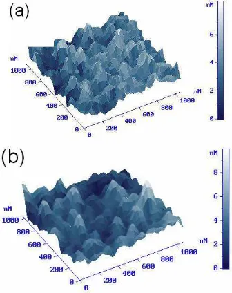
Figure 2 shows the AFM images of ZnO films grown with and without plasma surface pre-treatment. These images were taken at a 1000 x 1000 nm scan size. The corresponding surface roughness is 0.94 nm and 1.15 nm, respectively. It is found that the ZnO nanostructures prepared by plasma surface pre-treatment shows more uniform and smaller grain size as compared to those without the plasma surface pre-treatment. It implies that increasing the quality of surface morphology of films causes the surface becomes more polar are developed on the surface. Consequently, the surface can react more easily with the solution [4], [5], similar to the report of Shi et al.[6].
Applications to the transistors are also demonstrated as the current-voltage output characteristics shown in Fig. 3. The enhancement mode transistor with the threshold voltage of 20V exhibits good saturation transistor behavior. The drain saturation current of 38.1 µA at VGS = 35 V can be achieved. In
the saturation region, the calculated electron mobility is 4.44 cm2/V.s. The obtained I
on/Ioff and subthreshold slope of the transistor are 7.03 x 10⁵ and 2.5 V/dec, respectively. This
indicates that the plasma surface pre-treatment is effective for high quality ZnO films grown on plastic substrates [7].
Conclusions
The plasma surface pre-treatment is effective to improve the preparation of ZnO films on ITO-laminated PET plastic substrate. The enhancement of the ZnO nanostructure quality can be seen. The ZnO nanostructure enhancement mode transistor with good saturation behavior has been demonstrated.
Acknowledgments
This work was supported in part by the National Science Council of Taiwan under contract number NSC-98-2221-E- 006-213-MY3.
References
[1] J.P. Kim, S.A. Lee, J.S. Bae, S.K. Park, U.C. Choi, C.R. Cho, Thin Solid Films, vol. 516, no.16, pp.5223-5226, Jan. 2008.. [2] G. Zhang, M. Adachi, S. Ganjil, A. Nakamura, J. Temmyo, and Y.
Matsui, Jpn. J. Appl. Phys., vol. 46, no. 29, L730-732, July 2007. [3] K. Remashan, D. K. Hwang, S.D. Park, J.W. Bae, G.Y. Yeom, S. J. Park, and J. H. Jang, Electrochem. Solid-State Lett., vol. 11, no. 3, pp. H55-H59, Jan 2008.
[4] C. M Chan, Polymer Surface Modification and Characterization (Munich; Hanser; New York: Hanser), pp.237-238, 1994. [5] C.J. Huang, and W.C. Shih, J. Electronic Mat., vol. 32, no. 6, pp.
478-482, June 2003.
[6] D. Shi, and P. He, Rev. Adv .Mater. Sci., vol. 7, no. 2, pp 97-107, Sep. 2004.
[7] A.C. Mofor, A.S. Bakin, B. Postels, M. Suleiman, A. Elshaer and A. Waag, Thin Solid Films, vol. 516, no.7, pp..1401-1404, Feb.
2008.
Figure 1 X-rays diffraction patterns of 120 nm thick ZnO films deposited with and without plasma surface pre-treatment.
Figure 2 The AFM images of ZnO films (a) with and (b) without plasma surface pre-treatment.
Figure 3 IDS - VDS characteristics for a W/L=1500/150 µm ZnO