LAMPIRAN 1
: GAMBAR ALAT
Gambar 1. Spo2 Mindrey PM50
Gambar 2. Oksimeter
LAMPIRAN 2 : LISTING PROGRAM
CodeWizardAVR V1.25.5 Professional
© Copyright 1998-2007 Pavel Haiduc, HP InfoTech s.r.l.
Date : 05/06/2012
Author : Ook
Company : UNAIR
Chip type : ATmega16
Program type : Application
Clock frequency : 4,000000 MHz
Memory model : Small
External SRAM size : 0
Data Stack size : 256
*****************************************************/
#include <mega16.h>
// Alphanumeric LCD Module functions
#asm
.equ __lcd_port=0x18 ;PORTB
#endasm
#include <lcd.h>
#include <stdio.h>
#include <delay.h>
#define led PORTC.0
#define ir PORTC.1
#define sample_IR PORTC.3
bit t_count;
unsigned char lcd_buffer[33],lcd_buffer2[33],lcd_buffer3[33];
unsigned long temp,tempa,spo,v,vy,vin,vx,r,r1;
char pul1,sat1,kom1,pul,sat,kom,;
interrupt [TIM1_OVF] void timer1_ovf_isr(void)
{
// Reinitialize Timer 1 value
TCNT1H=0xF5;
TCNT1L=0x00;
if (t_count==1) {
led=1;
sample_led=1;
ir=0;
sample_IR=0;
t_count=0;
}
else {
led=0;
sample_led=0;
sample_IR=1;
ir=1;
t_count=1;
}
}
#define ADC_VREF_TYPE 0x00
// Read the AD conversion result
unsigned int read_adc(unsigned char adc_input)
{
ADMUX=adc_input | (ADC_VREF_TYPE & 0xff);
delay_us(10);
ADCSRA|=0x40;
while ((ADCSRA & 0x10)==0);
ADCSRA|=0x10;
return ADCW;
}
void tampilan_awal()
{
lcd_gotoxy(0,0);
lcd_putsf(" LapanTech ");
delay_ms(1500);
lcd_gotoxy(6,1);
lcd_putsf("Present ");
delay_ms(1500);
lcd_clear();
lcd_gotoxy(0,1);
lcd_putsf("PULSE OXYMETRI");
delay_ms(1500);
lcd_clear();
}
{
//===========ADC Sample LED=========//
temp=read_adc(0);
vx=temp*50;
//vy=vx/1024;
vy=temp/2;
pul=(vy/100)%10;
sat=(vy/10)%10;
kom=vy%10;
lcd_gotoxy(0,0);
lcd_putsf("LED:");
//sprintf(lcd_buffer,"%d%d,%d",pul,sat,kom);
sprintf(lcd_buffer,"%d",vy);
lcd_gotoxy(0,1);
lcd_puts(lcd_buffer);
delay_ms(300);
//===========ADC Sample IR==========//
tempa=read_adc(1);
vin=tempa*50;
//v=vin/1024;
v=tempa/20;
pul1=(v/100)%10;
sat1=(v/10)%10;
kom1=v%10;
lcd_putsf("IR:");
//sprintf(lcd_buffer2,"%d%d,%d",pul1,sat1,kom1);
sprintf(lcd_buffer2,"%d",v);
lcd_gotoxy(5,1);
lcd_puts(lcd_buffer2);
delay_ms(300);
//==========rumus=====
r=vy/v;
r1=r*20;
spo=1100-r1;
//===========buzzer=======
if (spo<850) {PORTD.0=1;
}
else {PORTD.0=0;
};
}
// Declare your global variables here
void main(void)
{
// Port A initialization
PORTA=0x00;
DDRA=0x00;
// Port B initialization
PORTB=0x00;
DDRB=0x00;
PORTC=0x00;
DDRC=0xff;
// Port D initialization
PORTD=0x00;
DDRD=0xff;
// Timer/Counter 0 initialization
// OC0 output: Disconnected
TCCR0=0x00;
TCNT0=0x00;
OCR0=0x00;
TCCR1A=0x00;
TCCR1B=0x05;
TCNT1H=0xD5;
TCNT1L=0xD0;
ICR1H=0x00;
ICR1L=0x00;
OCR1AH=0x00;
OCR1AL=0x00;
OCR1BH=0x00;
OCR1BL=0x00;
ASSR=0x00;
TCCR2=0x00;
TCNT2=0x00;
OCR2=0x00;
MCUCSR=0x00;
// Timer(s)/Counter(s) Interrupt(s) initialization
TIMSK=0x04;
ACSR=0x80;
SFIOR=0x00;
ADMUX=ADC_VREF_TYPE & 0xff;
ADCSRA=0x82;
// LCD module initialization
lcd_init(16);
// Global enable interrupts
#asm("sei")
t_count=0;
//tampilan_awal();
while (1)
{
// Place your code here
baca_adc();
//spo=vy/v;
pul=(spo/100)%10;
sat=(spo/10)%10;
kom=spo%10;
lcd_gotoxy(10,0);
sprintf(lcd_buffer3,"%d%d,%d",pul,sat,kom);
//sprintf(lcd_buffer3,"%d",r);
lcd_gotoxy(10,1);
lcd_puts(lcd_buffer3);
delay_ms(1000);
};
LF353
LF353 Wide Bandwidth Dual JFET Input Operational Amplifier
LF353
Wide Bandwidth Dual JFET Input Operational Amplifier
General Description
These devices are low cost, high speed, dual JFET input operational amplifiers with an internally trimmed input offset voltage (BI-FET II™ technology). They require low supply current yet maintain a large gain bandwidth product and fast slew rate. In addition, well matched high voltage JFET input devices provide very low input bias and offset currents. The LF353 is pin compatible with the standard LM1558 allowing designers to immediately upgrade the overall performance of existing LM1558 and LM358 designs.
These amplifiers may be used in applications such as high speed integrators, fast D/A converters, sample and hold circuits and many other circuits requiring low input offset voltage, low input bias current, high input impedance, high slew rate and wide bandwidth. The devices also exhibit low noise and offset voltage drift.
Features
n Internally trimmed offset voltage: 10 mV
n Low input bias current: 50pA
n Low input noise voltage: 25 nV/√Hz
n Low input noise current: 0.01 pA/√Hz
n Wide gain bandwidth: 4 MHz
n High slew rate: 13 V/µs
n Low supply current: 3.6 mA
n High input impedance: 1012Ω
n Low total harmonic distortion : ≤0.02%
n Low 1/f noise corner: 50 Hz
n Fast settling time to 0.01%: 2 µs
Typical Connection
Order Number LF353M, LF353MX or LF353N See NS Package Number M08A or N08E
If Military/Aerospace specified devices are required, please contact the National Semiconductor Sales Office/ Distributors for availability and specifications.
Supply Voltage ±18V
Power Dissipation (Note 2)
Operating Temperature Range 0˚C to +70˚C
Tj(MAX) 150˚C
Differential Input Voltage ±30V
Input Voltage Range (Note 3) ±15V
Output Short Circuit Duration Continuous
Storage Temperature Range −65˚C to +150˚C
Lead Temp. (Soldering, 10 sec.) 260˚C
Soldering Information Dual-In-Line Package
Soldering (10 sec.) 260˚C
Vapor Phase (60 sec.) 215˚C
Infrared (15 sec.) 220˚C
See AN-450 “Surface Mounting Methods and Their Effect on Product Reliability” for other methods of soldering surface mount devices.
ESD Tolerance (Note 8) 1000V
θJAM Package TBD
Note 1: Absolute Maximum Ratings indicate limits beyond which damage to the device may occur. Operating ratings indicate conditions for which the device is functional, but do not guarantee specific performance limits. Elec-trical Characteristics state DC and AC elecElec-trical specifications under particu-lar test conditions which guarantee specific performance limits. This assumes that the device is within the Operating Ratings. Specifications are not guar-anteed for parameters where no limit is given, however, the typical value is a good indication of device performance.
DC Electrical Characteristics
(Note 5)
Symbol Parameter Conditions LF353 Units
MIn Typ Max
VOS Input Offset Voltage RS=10kΩ, TA=25˚C 5 10 mV
Over Temperature 13 mV
∆VOS/∆T Average TC of Input Offset Voltage RS=10 kΩ 10 µV/˚C
Over Temperature 15 V/mV
VO Output Voltage Swing VS=±15V, RL=10kΩ ±12 ±13.5 V
VCM Input Common-Mode Voltage VS=±15V ±11 +15 V
Range −12 V
CMRR Common-Mode Rejection Ratio RS≤10kΩ 70 100 dB
PSRR Supply Voltage Rejection Ratio (Note 7) 70 100 dB
IS Supply Current 3.6 6.5 mA
AC Electrical Characteristics
(Note 5)
Symbol Parameter Conditions LF353 Units
Min Typ Max
Amplifier to Amplifier Coupling TA=25˚C, f=1 Hz−20 kHz −120 dB
(Input Referred)
SR Slew Rate VS=±15V, TA=25˚C 8.0 13 V/µs
GBW Gain Bandwidth Product VS=±15V, TA=25˚C 2.7 4 MHz
en Equivalent Input Noise Voltage TA=25˚C, RS=100Ω, 16
f=1000 Hz
in Equivalent Input Noise Current Tj=25˚C, f=1000 Hz 0.01
(Note 5)
Symbol Parameter Conditions LF353 Units
Min Typ Max
THD Total Harmonic Distortion AV=+10, RL=10k,
VO=20Vp−p, BW=20 Hz-20 kHz
<0.02 %
Note 2: For operating at elevated temperatures, the device must be derated based on a thermal resistance of 115˚C/W typ junction to ambient for the N package, and 158˚C/W typ junction to ambient for the H package.
Note 3: Unless otherwise specified the absolute maximum negative input voltage is equal to the negative power supply voltage. Note 4: The power dissipation limit, however, cannot be exceeded.
Note 5: These specifications apply for VS=±15V and 0˚C≤TA≤+70˚C. VOS, IBand IOSare measured at VCM=0.
Note 6: The input bias currents are junction leakage currents which approximately double for every 10˚C increase in the junction temperature, Tj. Due to the limited
production test time, the input bias currents measured are correlated to junction temperature. In normal operation the junction temperature rises above the ambient temperature as a result of internal power dissipation, PD. Tj=TA+θjAPDwhereθjAis the thermal resistance from junction to ambient. Use of a heat sink is
recommended if input bias current is to be kept to a minimum.
Note 7: Supply voltage rejection ratio is measured for both supply magnitudes increasing or decreasing simultaneously in accordance with common practice. VS
=±6V to±15V.
Note 8: Human body model, 1.5 kΩin series with 100 pF.
Typical Performance Characteristics
Input Bias Current Input Bias Current
00564918 00564919
Supply Current Positive Common-Mode Input Voltage Limit
00564920
Negative Common-Mode Input Voltage Limit Positive Current Limit
00564922 00564923
Negative Current Limit Voltage Swing
00564924 00564925
Output Voltage Swing Gain Bandwidth
00564926 00564927
Bode Plot Slew Rate
00564928 00564929
Distortion vs. Frequency Undistorted Output Voltage Swing
00564930 00564931
Open Loop Frequency Response Common-Mode Rejection Ratio
Power Supply Rejection Ratio Equivalent Input Noise Voltage
00564934 00564935
Open Loop Voltage Gain (V/V) Output Impedance
00564936 00564937
Inverter Settling Time
00564938
Small Signaling Inverting
00564904 Large Signal Inverting
00564906
00564905 Large Signal Non-Inverting
00564907
Current Limit (RL= 100Ω)
00564908
Application Hints
These devices are op amps with an internally trimmed input offset voltage and JFET input devices (BI-FET II). These JFETs have large reverse breakdown voltages from gate to source and drain eliminating the need for clamps across the inputs. Therefore, large differential input voltages can easily be accommodated without a large increase in input current.
supply voltages. However, neither of the input voltages should be allowed to exceed the negative supply as this will cause large currents to flow which can result in a destroyed unit.
since raising the input back within the common-mode range again puts the input stage and thus the amplifier in a normal operating mode.
Exceeding the positive common-mode limit on a single input will not change the phase of the output; however, if both inputs exceed the limit, the output of the amplifier will be forced to a high state.
The amplifiers will operate with a common-mode input volt-age equal to the positive supply; however, the gain band-width and slew rate may be decreased in this condition. When the negative common-mode voltage swings to within 3V of the negative supply, an increase in input offset voltage may occur.
Each amplifier is individually biased by a zener reference which allows normal circuit operation on ±6V power sup-plies. Supply voltages less than these may result in lower gain bandwidth and slew rate.
The amplifiers will drive a 2 kΩload resistance to±10V over the full temperature range of 0˚C to +70˚C. If the amplifier is forced to drive heavier load currents, however, an increase in input offset voltage may occur on the negative voltage swing and finally reach an active current limit on both posi-tive and negaposi-tive swings.
Precautions should be taken to ensure that the power supply for the integrated circuit never becomes reversed in polarity
forward diode within the IC could cause fusing of the internal conductors and result in a destroyed unit.
As with most amplifiers, care should be taken with lead dress, component placement and supply decoupling in order to ensure stability. For example, resistors from the output to an input should be placed with the body close to the input to minimize “pick-up” and maximize the frequency of the feed-back pole by minimizing the capacitance from the input to ground.
A feedback pole is created when the feedback around any amplifier is resistive. The parallel resistance and capacitance from the input of the device (usually the inverting input) to AC ground set the frequency of the pole. In many instances the frequency of this pole is much greater than the expected 3 dB frequency of the closed loop gain and consequently there is negligible effect on stability margin. However, if the feed-back pole is less than approximately 6 times the expected 3 dB frequency a lead capacitor should be placed from the output to the input of the op amp. The value of the added capacitor should be such that the RC time constant of this capacitor and the resistance it parallels is greater than or equal to the original feedback pole time constant.
Detailed Schematic
00564909
Three-Band Active Tone Control
00564939
00564940
Note 1:All controls flat.
Improved CMRR Instrumentation Amplifier
00564941
Fourth Order Low Pass Butterworth Filter
00564942
Fourth Order High Pass Butterworth Filter
Ohms to Volts Converter
00564944
Order Number LF353M or LF353MX NS Package Number M08A
Molded Dual-In-Line Package Order Number LF353N
LIFE SUPPORT POLICY
NATIONAL’S PRODUCTS ARE NOT AUTHORIZED FOR USE AS CRITICAL COMPONENTS IN LIFE SUPPORT DEVICES OR SYSTEMS WITHOUT THE EXPRESS WRITTEN APPROVAL OF THE PRESIDENT AND GENERAL COUNSEL OF NATIONAL SEMICONDUCTOR CORPORATION. As used herein:
1. Life support devices or systems are devices or systems which, (a) are intended for surgical implant into the body, or (b) support or sustain life, and whose failure to perform when properly used in accordance with instructions for use provided in the labeling, can be reasonably expected to result in a significant injury to the user.
2. A critical component is any component of a life support device or system whose failure to perform can be reasonably expected to cause the failure of the life support device or system, or to affect its safety or effectiveness.
BANNED SUBSTANCE COMPLIANCE
National Semiconductor certifies that the products and packing materials meet the provisions of the Customer Products Stewardship Specification (CSP-9-111C2) and the Banned Substances and Materials of Interest Specification (CSP-9-111S2) and contain no ‘‘Banned Substances’’ as defined in CSP-9-111S2.
National Semiconductor Americas Customer Support Center
Email: [email protected]
National Semiconductor Europe Customer Support Center
Fax: +49 (0) 180-530 85 86 Email: [email protected]
National Semiconductor Asia Pacific Customer Support Center
Email: [email protected]
National Semiconductor Japan Customer Support Center
Fax: 81-3-5639-7507 Email: [email protected]
LF353
W
ide
Bandwidth
Dual
JFET
Input
Operational
IMPORTANT NOTICE
Texas Instruments Incorporated and its subsidiaries (TI) reserve the right to make corrections, modifications, enhancements, improvements, and other changes to its products and services at any time and to discontinue any product or service without notice. Customers should obtain the latest relevant information before placing orders and should verify that such information is current and complete. All products are sold subject to TI’s terms and conditions of sale supplied at the time of order acknowledgment.
TI warrants performance of its hardware products to the specifications applicable at the time of sale in accordance with TI’s standard warranty. Testing and other quality control techniques are used to the extent TI deems necessary to support this warranty. Except where mandated by government requirements, testing of all parameters of each product is not necessarily performed.
TI assumes no liability for applications assistance or customer product design. Customers are responsible for their products and applications using TI components. To minimize the risks associated with customer products and applications, customers should provide adequate design and operating safeguards.
TI does not warrant or represent that any license, either express or implied, is granted under any TI patent right, copyright, mask work right, or other TI intellectual property right relating to any combination, machine, or process in which TI products or services are used. Information published by TI regarding third-party products or services does not constitute a license from TI to use such products or services or a warranty or endorsement thereof. Use of such information may require a license from a third party under the patents or other intellectual property of the third party, or a license from TI under the patents or other intellectual property of TI.
Reproduction of TI information in TI data books or data sheets is permissible only if reproduction is without alteration and is accompanied by all associated warranties, conditions, limitations, and notices. Reproduction of this information with alteration is an unfair and deceptive business practice. TI is not responsible or liable for such altered documentation. Information of third parties may be subject to additional restrictions.
Resale of TI products or services with statements different from or beyond the parameters stated by TI for that product or service voids all express and any implied warranties for the associated TI product or service and is an unfair and deceptive business practice. TI is not responsible or liable for any such statements.
TI products are not authorized for use in safety-critical applications (such as life support) where a failure of the TI product would reasonably be expected to cause severe personal injury or death, unless officers of the parties have executed an agreement specifically governing such use. Buyers represent that they have all necessary expertise in the safety and regulatory ramifications of their applications, and acknowledge and agree that they are solely responsible for all legal, regulatory and safety-related requirements concerning their products and any use of TI products in such safety-critical applications, notwithstanding any applications-related information or support that may be provided by TI. Further, Buyers must fully indemnify TI and its representatives against any damages arising out of the use of TI products in such safety-critical applications.
TI products are neither designed nor intended for use in military/aerospace applications or environments unless the TI products are specifically designated by TI as military-grade or"enhanced plastic."Only products designated by TI as military-grade meet military specifications. Buyers acknowledge and agree that any such use of TI products which TI has not designated as military-grade is solely at the Buyer's risk, and that they are solely responsible for compliance with all legal and regulatory requirements in connection with such use. TI products are neither designed nor intended for use in automotive applications or environments unless the specific TI products are designated by TI as compliant with ISO/TS 16949 requirements. Buyers acknowledge and agree that, if they use any non-designated products in automotive applications, TI will not be responsible for any failure to meet such requirements.
Following are URLs where you can obtain information on other Texas Instruments products and application solutions:
Products Applications
Audio www.ti.com/audio Communications and Telecom www.ti.com/communications Amplifiers amplifier.ti.com Computers and Peripherals www.ti.com/computers Data Converters dataconverter.ti.com Consumer Electronics www.ti.com/consumer-apps DLP®Products www.dlp.com Energy and Lighting www.ti.com/energy
DSP dsp.ti.com Industrial www.ti.com/industrial
Clocks and Timers www.ti.com/clocks Medical www.ti.com/medical
Interface interface.ti.com Security www.ti.com/security
Logic logic.ti.com Space, Avionics and Defense www.ti.com/space-avionics-defense Power Mgmt power.ti.com Transportation and Automotive www.ti.com/automotive
Microcontrollers microcontroller.ti.com Video and Imaging www.ti.com/video
RFID www.ti-rfid.com
OMAP Mobile Processors www.ti.com/omap
Wireless Connectivity www.ti.com/wirelessconnectivity
TI E2E Community Home Page e2e.ti.com
SCHS051D – NOVEMBER 1998 – REVISED SEPTEMBER 2003
D
15-V Digital or ±7.5-V Peak-to-PeakSwitching
D
125-Ω Typical On-State Resistance for 15-VOperation
D
Switch On-State Resistance Matched toWithin 5 Ω Over 15-V Signal-Input Range
D
On-State Resistance Flat Over FullPeak-to-Peak Signal Range
D
High On/Off Output-Voltage Ratio: 80 dBTypical at fis = 10 kHz, RL = 1 kΩ
D
High Degree of Linearity: <0.5% DistortionTypical at fis = 1 kHz, Vis = 5 V p-p, VDD – VSS≥ 10 V, RL = 10 kΩ
D
Extremely Low Off-State Switch Leakage,Resulting in Very Low Offset Current and High Effective Off-State Resistance: 10 pA Typical at VDD – VSS = 10 V, TA = 25°C
D
Extremely High Control Input Impedance(Control Circuit Isolated From Signal Circuit): 1012 Ω Typical
D
Low Crosstalk Between Switches: –50 dBTypical at fis = 8 MHz, RL = 1 kΩ
D
Matched Control-Input to Signal-OutputCapacitance: Reduces Output Signal Transients
D
Frequency Response, Switch On = 40 MHzTypical
D
100% Tested for Quiescent Current at 20 VD
5-V, 10-V, and 15-V Parametric RatingsD
Meets All Requirements of JEDEC TentativeStandard No. 13-B, Standard Specifications
for Description of “B” Series CMOS Devices
D
Applications:– Analog Signal Switching/Multiplexing: Signal Gating, Modulator, Squelch Control, Demodulator, Chopper, Commutating Switch
– Digital Signal Switching/Multiplexing – Transmission-Gate Logic Implementation – Analog-to-Digital and Digital-to-Analog
Conversion
– Digital Control of Frequency, Impedance, Phase, and Analog-Signal Gain
description/ordering information
The CD4066B is a quad bilateral switch intended for the transmission or multiplexing of analog or digital signals. It is pin-for-pin compatible with the CD4016B, but exhibits a much lower on-state resistance. In addition, the on-state resistance is relatively constant over the full signal-input range.
The CD4066B consists of four bilateral switches, each with independent controls. Both the p and the n devices in a given switch are biased on or off simultaneously by the control signal. As shown in Figure 1, the well of the n-channel device on each switch is tied to either the input (when the switch is on) or to VSS (when the switch is off). This configuration eliminates the variation of the switch-transistor threshold voltage with input signal and, thus, keeps the on-state resistance low over the full operating-signal range.
The advantages over single-channel switches include peak input-signal voltage swings equal to the full supply voltage and more constant on-state impedance over the input-signal range. However, for sample-and-hold applications, the CD4016B is recommended.
Please be aware that an important notice concerning availability, standard warranty, and use in critical applications of Texas Instruments semiconductor products and disclaimers thereto appears at the end of this data sheet.
SCHS051D – NOVEMBER 1998 – REVISED SEPTEMBER 2003
description/ordering information (continued)
ORDERING INFORMATION
TA PACKAGE† ORDERABLE
PART NUMBER
TOP-SIDE MARKING
–55 C to 125 C
CDIP – F Tube of 25 CD4066BF3A CD4066BF3A
–55 C to 125 C
PDIP – E Tube of 25 CD4066BE CD4066BE
–55 C to 125 C SOIC – M
Tube of 50 CD4066BM
CD4066BM
–55°C to 125°C SOIC – M Reel of 2500 CD4066BM96 CD4066BM
–55°C to 125°C
Reel of 250 CD4066BMT
SOP – NS Reel of 2000 CD4066BNSR CD4066B
TSSOP – PW Tube of 90 CD4066BPW CM066B
TSSOP – PW
Reel of 2000 CD4066BPWR CM066B
† Package drawings, standard packing quantities, thermal data, symbolization, and PCB design guidelines are available at www.ti.com/sc/package.
† All control inputs are protected by the CMOS protection network. NOTES: A. All p substrates are connected to VDD.
B. Normal operation control-line biasing: switch on (logic 1), VC = VDD; switch off (logic 0), VC = VSS
C. Signal-level range: VSS ≤Vis ≤ VDD
Control VC†
VDD VSS
VSS
n
n
p
Out Vos Control
Switch
In
92CS-29113 n
p
Vis
SCHS051D – NOVEMBER 1998 – REVISED SEPTEMBER 2003
absolute maximum ratings over operating free-air temperature (unless otherwise noted)
†DC supply-voltage range, VDD (voltages referenced to VSS terminal) . . . –0.5 V to 20 V Input voltage range, Vis (all inputs) . . . –0.5 V to VDD+ 0.5 V DC input current, IIN (any one input) . . . ±10 mA Package thermal impedance, θJA (see Note 1): E package . . . 80°C/W M package . . . 86°C/W NS package . . . 76°C/W PW package . . . 113°C/W Lead temperature (during soldering):
At distance 1/16 ±1/32 inch (1,59 ±0,79 mm) from case for 10 s max . . . 265°C Storage temperature range, Tstg –65. . . °C to 150°C
† Stresses beyond those listed under “absolute maximum ratings” may cause permanent damage to the device. These are stress ratings only, and functional operation of the device at these or any other conditions beyond those indicated under “recommended operating conditions” is not implied. Exposure to absolute-maximum-rated conditions for extended periods may affect device reliability.
NOTE 1: The package thermal impedance is calculated in accordance with JESD 51-7.
recommended operating conditions
MIN MAX UNIT
VDD Supply voltage 3 18 V
SCHS051D – NOVEMBER 1998 – REVISED SEPTEMBER 2003
electrical characteristics
PARAMETER TEST CONDITIONS
LIMITS AT INDICATED TEMPERATURES
UNIT
PARAMETER TEST CONDITIONS VIN VDD
–55°C –40°C 85°C 125°C 25°C UNIT
IDD Quiescent devicecurrent
0, 15 15 1 1 30 30 0.01 1 µA
0, 20 20 5 5 150 150 0.02 5
Signal Inputs (Vis) and Outputs (Vos)
r On-state resistance
VC = VDD,
RL = 10 kΩ returned 5 800 850 1200 1300 470 1050
ron On-state resistance(max)
RL = 10 k returned
Propagation delay RL = 200 k
Ω, VC = VDD,
(square wave centered on 5 V),
10 10 20 ns
signal output) (square wave centered on 5 V),
tr, tf = 20 ns 15 7 15
Cis Input capacitance VDD = 5 V, VC = VSS = –5 V 8 pF
Cos Output capacitance VDD = 5 V, VC = VSS = –5 V 8 pF
SCHS051D – NOVEMBER 1998 – REVISED SEPTEMBER 2003
electrical characteristics (continued)
CHARACTERISTIC TEST CONDITIONS
LIMITS AT INDICATED TEMPERATURES
UNIT
CHARACTERISTIC TEST CONDITIONS VDD
–55°C –40°C 85°C 125°C 25°C UNIT VILC Control input, low voltage (max) |Iis| < 10
µA,
Vis = VSS, VOS = VDD, and
V = V , V = V
10 2 2 2 2 2 V
ILC low voltage (max) is SS OS DD
Vis = VDD, VOS = VSS 15 2 2 2 2 2
V Control input, See Figure 6
5 3.5 (MIN)
V
VIHCIHC Control input, high voltage See Figure 6 10 7 (MIN) V
high voltage
CI Input capacitance 5 7.5 pF
switching characteristics
Iis (mA) OUTPUT, Vos(V)
SCHS051D – NOVEMBER 1998 – REVISED SEPTEMBER 2003
TYPICAL CHARACTERISTICS
Vis – Input Signal Voltage – V 600
TYPICAL ON-STATE RESISTANCE vs
INPUT SIGNAL VOLTAGE (ALL TYPES)
92CS-27326RI
– Channel On-State Resistance –
on
INPUT SIGNAL VOLTAGE (ALL TYPES)
300
Vis – Input Signal Voltage – V +25°C
–55°C
92CS-27327RI
– Channel On-State Resistance –
on
Ω
r
Vis – Input Signal Voltage – V TYPICAL ON-STATE RESISTANCE
vs
INPUT SIGNAL VOLTAGE (ALL TYPES)
Figure 4
– Channel On-State Resistance –
on
Ω
r
Vis – Input Signal Voltage – V
Figure 5
TYPICAL ON-STATE RESISTANCE vs
INPUT SIGNAL VOLTAGE (ALL TYPES)
600
– Channel On-State Resistance –
on
Ω
SCHS051D – NOVEMBER 1998 – REVISED SEPTEMBER 2003
TYPICAL CHARACTERISTICS
CD4066B 1 of 4 Switches Iis
Figure 6. Determination of ron as a Test Condition for Control-Input High-Voltage (VIHC) Specification
X-Y
Figure 7. Channel On-State Resistance Measurement Circuit
Figure 8
TYPICAL ON CHARACTERISTICS FOR 1 OF 4 CHANNELS
3
All unused terminals are connected to VSS
f – Switching Frequency – kHz POWER DISSIPATION PER PACKAGE
vs
SWITCHING FREQUENCY
TA = 25°C
Power Dissipation Per Package – W
SCHS051D – NOVEMBER 1998 – REVISED SEPTEMBER 2003
Measured on Boonton capacitance bridge, model 75a (1 MHz); test-fixture capacitance nulled out.
92CS-30921
Figure 10. Typical On Characteristics for One of Four Channels
VDD
Figure 11. Off-Switch Input or Output Leakage
All unused terminals are connected to VSS.
VDD
Figure 12. Propagation Delay Time Signal Input (Vis) to Signal Output (Vos)
All unused terminals are connected to VSS.
VDD
Figure 13. Crosstalk-Control Input to Signal Output
SCHS051D – NOVEMBER 1998 – REVISED SEPTEMBER 2003
TYPICAL CHARACTERISTICS
VDD VC = VDD
Vos
VSS CD4066B
1 of 4 Switches VDD
92CS-30925 1 kΩ
50 pF VDD
NOTES: A. All unused terminals are connected to VSS.
B. Delay is measured at Vos level of +10% from ground (turn-on) or on-state output level (turn-off). tr = tf = 20 ns
Figure 14. Propagation Delay, tPLH, tPHL Control-Signal Output
VDD = 10 V VC
VSS CD4066B
1 of 4 Switches Vis = 10 V
92CS-30925 1 kΩ
50 pF tr = tf = 20 ns
VC
Vos
90% 10%
All unused terminals are connected to VSS.
VOS+VOSat 1 kHz
2
VOS+VOS at 1 kHz
2 Repetition
Rate 50%
tr tf
10 V
0 V
SCHS051D – NOVEMBER 1998 – REVISED SEPTEMBER 2003
TYPICAL CHARACTERISTICS
Inputs
VSS
Measure inputs sequentially to both VDD and VSS. Connect all unused inputs to either VDD or VSS. Measure control inputs only.
I
VSS VDD
92CS-27555
Figure 16. Input Leakage-Current Test Circuit
VDD
1/6 CD4049B 10 k
Signal
SCHS051D – NOVEMBER 1998 – REVISED SEPTEMBER 2003
TYPICAL CHARACTERISTICS
SWA
SWB
SWC
SWD
92CS-30927 Analog Inputs (±5 V)
VDD = 5 V VDD = 5 V
5 V
–5 V
5 V CD4066B
Analog Outputs (±5 V) VSS = –5 V CD4054B
VSS = 0 V VEE = –5 V IN
0
Digital Control Inputs
0
SCHS051D – NOVEMBER 1998 – REVISED SEPTEMBER 2003
APPLICATION INFORMATION
In applications that employ separate power sources to drive VDD and the signal inputs, the VDD current capability should exceed VDD/RL (RL = effective external load of the four CD4066B bilateral switches). This provision avoids any permanent current flow or clamp action on the VDD supply when power is applied or removed from the CD4066B.
In certain applications, the external load-resistor current can include both VDD and signal-line components. To avoid drawing VDD current when switch current flows into terminals 1, 4, 8, or 11, the voltage drop across the bidirectional switch must not exceed 0.8 V (calculated from ron values shown).
PACKAGING INFORMATION
Orderable Device Status(1) Package Type
Package Drawing
Pins Package Qty
Eco Plan(2) Lead/Ball Finish MSL Peak Temp(3)
CD4066BE ACTIVE PDIP N 14 25 Pb-Free
(RoHS)
CU NIPDAU Level-NC-NC-NC
CD4066BEE4 ACTIVE PDIP N 14 25 Pb-Free
(RoHS)
CU NIPDAU Level-NC-NC-NC
CD4066BF ACTIVE CDIP J 14 1 TBD Call TI Level-NC-NC-NC
CD4066BF3A ACTIVE CDIP J 14 1 TBD Call TI Level-NC-NC-NC
CD4066BM ACTIVE SOIC D 14 50 Green (RoHS &
no Sb/Br)
CU NIPDAU Level-1-260C-UNLIM
CD4066BM96 ACTIVE SOIC D 14 2500 Green (RoHS &
no Sb/Br)
CU NIPDAU Level-1-260C-UNLIM CD4066BM96E4 ACTIVE SOIC D 14 2500 Green (RoHS &
no Sb/Br)
CU NIPDAU Level-1-260C-UNLIM
CD4066BME4 ACTIVE SOIC D 14 50 Green (RoHS &
no Sb/Br)
CU NIPDAU Level-1-260C-UNLIM
CD4066BMT ACTIVE SOIC D 14 250 Green (RoHS &
no Sb/Br)
CU NIPDAU Level-1-260C-UNLIM
CD4066BMTE4 ACTIVE SOIC D 14 250 Green (RoHS &
no Sb/Br)
CU NIPDAU Level-1-260C-UNLIM
CD4066BNSR ACTIVE SO NS 14 2000 Green (RoHS &
no Sb/Br)
CU NIPDAU Level-1-260C-UNLIM CD4066BNSRE4 ACTIVE SO NS 14 2000 Green (RoHS &
no Sb/Br)
CU NIPDAU Level-1-260C-UNLIM
CD4066BPW ACTIVE TSSOP PW 14 90 Green (RoHS &
no Sb/Br)
CU NIPDAU Level-1-260C-UNLIM CD4066BPWG4 ACTIVE TSSOP PW 14 90 Green (RoHS &
no Sb/Br)
CU NIPDAU Level-1-260C-UNLIM CD4066BPWR ACTIVE TSSOP PW 14 2000 Green (RoHS &
no Sb/Br)
CU NIPDAU Level-1-260C-UNLIM CD4066BPWRG4 ACTIVE TSSOP PW 14 2000 Green (RoHS &
no Sb/Br)
CU NIPDAU Level-1-260C-UNLIM
JM38510/05852BCA ACTIVE CDIP J 14 1 TBD Call TI Level-NC-NC-NC
(1)The marketing status values are defined as follows:
ACTIVE:Product device recommended for new designs.
LIFEBUY:TI has announced that the device will be discontinued, and a lifetime-buy period is in effect.
NRND:Not recommended for new designs. Device is in production to support existing customers, but TI does not recommend using this part in a new design.
PREVIEW:Device has been announced but is not in production. Samples may or may not be available. OBSOLETE:TI has discontinued the production of the device.
(2)
Eco Plan - The planned eco-friendly classification: Pb-Free (RoHS) or Green (RoHS & no Sb/Br) - please check http://www.ti.com/productcontentfor the latest availability information and additional product content details.
TBD:The Pb-Free/Green conversion plan has not been defined.
Pb-Free (RoHS):TI's terms "Lead-Free" or "Pb-Free" mean semiconductor products that are compatible with the current RoHS requirements for all 6 substances, including the requirement that lead not exceed 0.1% by weight in homogeneous materials. Where designed to be soldered at high temperatures, TI Pb-Free products are suitable for use in specified lead-free processes.
Green (RoHS & no Sb/Br):TI defines "Green" to mean Pb-Free (RoHS compatible), and free of Bromine (Br) and Antimony (Sb) based flame retardants (Br or Sb do not exceed 0.1% by weight in homogeneous material)
(3) MSL, Peak Temp. -- The Moisture Sensitivity Level rating according to the JEDEC industry standard classifications, and peak solder
temperature.
Important Information and Disclaimer:The information provided on this page represents TI's knowledge and belief as of the date that it is provided. TI bases its knowledge and belief on information provided by third parties, and makes no representation or warranty as to the accuracy of such information. Efforts are underway to better integrate information from third parties. TI has taken and continues to take reasonable steps to provide representative and accurate information but may not have conducted destructive testing or chemical analysis on incoming materials and chemicals. TI and TI suppliers consider certain information to be proprietary, and thus CAS numbers and other limited information may not be available for release.
In no event shall TI's liability arising out of such information exceed the total purchase price of the TI part(s) at issue in this document sold by TI to Customer on an annual basis.
MTSS001C – JANUARY 1995 – REVISED FEBRUARY 1999
PW (R-PDSO-G**) PLASTIC SMALL-OUTLINE PACKAGE
14 PINS SHOWN
NOTES: A. All linear dimensions are in millimeters. B. This drawing is subject to change without notice.
IMPORTANT NOTICE
Texas Instruments Incorporated and its subsidiaries (TI) reserve the right to make corrections, modifications, enhancements, improvements, and other changes to its products and services at any time and to discontinue any product or service without notice. Customers should obtain the latest relevant information before placing orders and should verify that such information is current and complete. All products are sold subject to TI’s terms and conditions of sale supplied at the time of order acknowledgment.
TI warrants performance of its hardware products to the specifications applicable at the time of sale in accordance with TI’s standard warranty. Testing and other quality control techniques are used to the extent TI deems necessary to support this warranty. Except where mandated by government requirements, testing of all parameters of each product is not necessarily performed.
TI assumes no liability for applications assistance or customer product design. Customers are responsible for their products and applications using TI components. To minimize the risks associated with customer products and applications, customers should provide adequate design and operating safeguards.
TI does not warrant or represent that any license, either express or implied, is granted under any TI patent right, copyright, mask work right, or other TI intellectual property right relating to any combination, machine, or process in which TI products or services are used. Information published by TI regarding third-party products or services does not constitute a license from TI to use such products or services or a warranty or endorsement thereof. Use of such information may require a license from a third party under the patents or other intellectual property of the third party, or a license from TI under the patents or other intellectual property of TI.
Reproduction of information in TI data books or data sheets is permissible only if reproduction is without alteration and is accompanied by all associated warranties, conditions, limitations, and notices. Reproduction of this information with alteration is an unfair and deceptive business practice. TI is not responsible or liable for such altered documentation.
Resale of TI products or services with statements different from or beyond the parameters stated by TI for that product or service voids all express and any implied warranties for the associated TI product or service and is an unfair and deceptive business practice. TI is not responsible or liable for any such statements.
Following are URLs where you can obtain information on other Texas Instruments products and application solutions:
Products Applications
Amplifiers amplifier.ti.com Audio www.ti.com/audio
Data Converters dataconverter.ti.com Automotive www.ti.com/automotive
DSP dsp.ti.com Broadband www.ti.com/broadband
Interface interface.ti.com Digital Control www.ti.com/digitalcontrol
Logic logic.ti.com Military www.ti.com/military
Power Mgmt power.ti.com Optical Networking www.ti.com/opticalnetwork
Microcontrollers microcontroller.ti.com Security www.ti.com/security
Telephony www.ti.com/telephony
Video & Imaging www.ti.com/video
Wireless www.ti.com/wireless
Mailing Address: Texas Instruments
Post Office Box 655303 Dallas, Texas 75265
Features
• High-performance, Low-power Atmel® AVR® 8-bit Microcontroller
• Advanced RISC Architecture
– 131 Powerful Instructions – Most Single-clock Cycle Execution – 32 x 8 General Purpose Working Registers
– Fully Static Operation
– Up to 16 MIPS Throughput at 16 MHz – On-chip 2-cycle Multiplier
• High Endurance Non-volatile Memory segments
– 16 Kbytes of In-System Self-programmable Flash program memory – 512 Bytes EEPROM
– 1 Kbyte Internal SRAM
– Write/Erase Cycles: 10,000 Flash/100,000 EEPROM
– Data retention: 20 years at 85°C/100 years at 25°C(1)
– Optional Boot Code Section with Independent Lock Bits In-System Programming by On-chip Boot Program True Read-While-Write Operation
– Programming Lock for Software Security
• JTAG (IEEE std. 1149.1 Compliant) Interface
– Boundary-scan Capabilities According to the JTAG Standard – Extensive On-chip Debug Support
– Programming of Flash, EEPROM, Fuses, and Lock Bits through the JTAG Interface
• Peripheral Features
– Two 8-bit Timer/Counters with Separate Prescalers and Compare Modes
– One 16-bit Timer/Counter with Separate Prescaler, Compare Mode, and Capture Mode
– Real Time Counter with Separate Oscillator – Four PWM Channels
– 8-channel, 10-bit ADC 8 Single-ended Channels
7 Differential Channels in TQFP Package Only
2 Differential Channels with Programmable Gain at 1x, 10x, or 200x – Byte-oriented Two-wire Serial Interface
– Programmable Serial USART – Master/Slave SPI Serial Interface
– Programmable Watchdog Timer with Separate On-chip Oscillator – On-chip Analog Comparator
• Special Microcontroller Features
– Power-on Reset and Programmable Brown-out Detection – Internal Calibrated RC Oscillator
– External and Internal Interrupt Sources
– Six Sleep Modes: Idle, ADC Noise Reduction, Power-save, Power-down, Standby and Extended Standby
• I/O and Packages
– 32 Programmable I/O Lines
– 40-pin PDIP, 44-lead TQFP, and 44-pad QFN/MLF
• Operating Voltages
– 2.7V - 5.5V for ATmega16L – 4.5V - 5.5V for ATmega16
• Speed Grades
– 0 - 8 MHz for ATmega16L – 0 - 16 MHz for ATmega16
• Power Consumption @ 1 MHz, 3V, and 25°C for ATmega16L
– Active: 1.1 mA – Idle Mode: 0.35 mA – Power-down Mode: < 1 µA
8-bit
Microcontroller
Pin
Configurations
Figure 1. Pinout ATmega16
Disclaimer
Typical values contained in this datasheet are based on simulations and characterization of other AVR microcontrollers manufactured on the same process technology. Min and Max values will be available after the device is characterized.(XCK/T0) PB0
Overview
The ATmega16 is a low-power CMOS 8-bit microcontroller based on the AVR enhanced RISC architecture. By executing powerful instructions in a single clock cycle, the ATmega16 achieves throughputs approaching 1 MIPS per MHz allowing the system designer to optimize power con-sumption versus processing speed.Block Diagram
Figure 2. Block DiagramThe AVR core combines a rich instruction set with 32 general purpose working registers. All the 32 registers are directly connected to the Arithmetic Logic Unit (ALU), allowing two independent registers to be accessed in one single instruction executed in one clock cycle. The resulting architecture is more code efficient while achieving throughputs up to ten times faster than con-ventional CISC microcontrollers.
The ATmega16 provides the following features: 16 Kbytes of In-System Programmable Flash Program memory with Read-While-Write capabilities, 512 bytes EEPROM, 1 Kbyte SRAM, 32 general purpose I/O lines, 32 general purpose working registers, a JTAG interface for Boundary-scan, On-chip Debugging support and programming, three flexible Timer/Counters with com-pare modes, Internal and External Interrupts, a serial programmable USART, a byte oriented Two-wire Serial Interface, an 8-channel, 10-bit ADC with optional differential input stage with programmable gain (TQFP package only), a programmable Watchdog Timer with Internal Oscil-lator, an SPI serial port, and six software selectable power saving modes. The Idle mode stops the CPU while allowing the USART, Two-wire interface, A/D Converter, SRAM, Timer/Counters, SPI port, and interrupt system to continue functioning. The Power-down mode saves the register contents but freezes the Oscillator, disabling all other chip functions until the next External Inter-rupt or Hardware Reset. In Power-save mode, the Asynchronous Timer continues to run, allowing the user to maintain a timer base while the rest of the device is sleeping. The ADC Noise Reduction mode stops the CPU and all I/O modules except Asynchronous Timer and ADC, to minimize switching noise during ADC conversions. In Standby mode, the crystal/reso-nator Oscillator is running while the rest of the device is sleeping. This allows very fast start-up combined with low-power consumption. In Extended Standby mode, both the main Oscillator and the Asynchronous Timer continue to run.
The device is manufactured using Atmel’s high density nonvolatile memory technology. The On-chip ISP Flash allows the program memory to be reprogrammed in-system through an SPI serial interface, by a conventional nonvolatile memory programmer, or by an On-chip Boot program running on the AVR core. The boot program can use any interface to download the application program in the Application Flash memory. Software in the Boot Flash section will continue to run while the Application Flash section is updated, providing true Read-While-Write operation. By combining an 8-bit RISC CPU with In-System Self-Programmable Flash on a monolithic chip, the Atmel ATmega16 is a powerful microcontroller that provides a highly-flexible and cost-effec-tive solution to many embedded control applications.
The ATmega16 AVR is supported with a full suite of program and system development tools including: C compilers, macro assemblers, program debugger/simulators, in-circuit emulators, and evaluation kits.
Pin Descriptions
VCC Digital supply voltage.
GND Ground.
Port A (PA7..PA0) Port A serves as the analog inputs to the A/D Converter.
Port B (PB7..PB0) Port B is an 8-bit bi-directional I/O port with internal pull-up resistors (selected for each bit). The Port B output buffers have symmetrical drive characteristics with both high sink and source capability. As inputs, Port B pins that are externally pulled low will source current if the pull-up resistors are activated. The Port B pins are tri-stated when a reset condition becomes active, even if the clock is not running.
Port B also serves the functions of various special features of the ATmega16 as listed on page 58.
Port C (PC7..PC0) Port C is an 8-bit bi-directional I/O port with internal pull-up resistors (selected for each bit). The Port C output buffers have symmetrical drive characteristics with both high sink and source capability. As inputs, Port C pins that are externally pulled low will source current if the pull-up resistors are activated. The Port C pins are tri-stated when a reset condition becomes active, even if the clock is not running. If the JTAG interface is enabled, the pull-up resistors on pins PC5(TDI), PC3(TMS) and PC2(TCK) will be activated even if a reset occurs.
Port C also serves the functions of the JTAG interface and other special features of the ATmega16 as listed on page 61.
Port D (PD7..PD0) Port D is an 8-bit bi-directional I/O port with internal pull-up resistors (selected for each bit). The Port D output buffers have symmetrical drive characteristics with both high sink and source capability. As inputs, Port D pins that are externally pulled low will source current if the pull-up resistors are activated. The Port D pins are tri-stated when a reset condition becomes active, even if the clock is not running.
Port D also serves the functions of various special features of the ATmega16 as listed on page 63.
RESET Reset Input. A low level on this pin for longer than the minimum pulse length will generate a reset, even if the clock is not running. The minimum pulse length is given in Table 15 on page 38. Shorter pulses are not guaranteed to generate a reset.
XTAL1 Input to the inverting Oscillator amplifier and input to the internal clock operating circuit.
XTAL2 Output from the inverting Oscillator amplifier.
AVCC AVCC is the supply voltage pin for Port A and the A/D Converter. It should be externally con-nected to VCC, even if the ADC is not used. If the ADC is used, it should be connected to VCC through a low-pass filter.
Resources
A comprehensive set of development tools, application notes and datasheets are available for download on http://www.atmel.com/avr.Note: 1.
About Code
Examples
AVR CPU Core
Introduction
This section discusses the AVR core architecture in general. The main function of the CPU coreis to ensure correct program execution. The CPU must therefore be able to access memories, perform calculations, control peripherals, and handle interrupts.
Architectural
Overview
Figure 3. Block Diagram of the AVR MCU Architecture
In order to maximize performance and parallelism, the AVR uses a Harvard architecture – with separate memories and buses for program and data. Instructions in the program memory are executed with a single level pipelining. While one instruction is being executed, the next instruc-tion is pre-fetched from the program memory. This concept enables instrucinstruc-tions to be executed in every clock cycle. The program memory is In-System Reprogrammable Flash memory.
The fast-access Register File contains 32 × 8-bit general purpose working registers with a single clock cycle access time. This allows single-cycle Arithmetic Logic Unit (ALU) operation. In a typ-ical ALU operation, two operands are output from the Register File, the operation is executed, and the result is stored back in the Register File – in one clock cycle.
Six of the 32 registers can be used as three 16-bit indirect address register pointers for Data Space addressing – enabling efficient address calculations. One of the these address pointers can also be used as an address pointer for look up tables in Flash Program memory. These added function registers are the 16-bit X-register, Y-register, and Z-register, described later in this section.
The ALU supports arithmetic and logic operations between registers or between a constant and a register. Single register operations can also be executed in the ALU. After an arithmetic opera-tion, the Status Register is updated to reflect information about the result of the operation.
Flash
Direct Addressing Indirect Addressing
Program flow is provided by conditional and unconditional jump and call instructions, able to directly address the whole address space. Most AVR instructions have a single 16-bit word for-mat. Every program memory address contains a 16-bit or 32-bit instruction.
Program Flash memory space is divided in two sections, the Boot program section and the Application Program section. Both sections have dedicated Lock bits for write and read/write protection. The SPM instruction that writes into the Application Flash memory section must reside in the Boot Program section.
During interrupts and subroutine calls, the return address Program Counter (PC) is stored on the Stack. The Stack is effectively allocated in the general data SRAM, and consequently the Stack size is only limited by the total SRAM size and the usage of the SRAM. All user programs must initialize the SP in the reset routine (before subroutines or interrupts are executed). The Stack Pointer SP is read/write accessible in the I/O space. The data SRAM can easily be accessed through the five different addressing modes supported in the AVR architecture.
The memory spaces in the AVRarchitecture are all linear and regular memory maps.
A flexible interrupt module has its control registers in the I/O space with an additional global interrupt enable bit in the Status Register. All interrupts have a separate interrupt vector in the interrupt vector table. The interrupts have priority in accordance with their interrupt vector posi-tion. The lower the interrupt vector address, the higher the priority.
The I/O memory space contains 64 addresses for CPU peripheral functions as Control Regis-ters, SPI, and other I/O functions. The I/O Memory can be accessed directly, or as the Data Space locations following those of the Register File, $20 - $5F.
ALU – Arithmetic
Logic Unit
The high-performance AVR ALU operates in direct connection with all the 32 general purpose working registers. Within a single clock cycle, arithmetic operations between general purpose registers or between a register and an immediate are executed. The ALU operations are divided into three main categories – arithmetic, logical, and bit-functions. Some implementations of the architecture also provide a powerful multiplier supporting both signed/unsigned multiplication and fractional format. See the “Instruction Set” section for a detailed description.
Status Register
The Status Register contains information about the result of the most recently executedarithme-tic instruction. This information can be used for altering program flow in order to perform conditional operations. Note that the Status Register is updated after all ALU operations, as specified in the Instruction Set Reference. This will in many cases remove the need for using the dedicated compare instructions, resulting in faster and more compact code.
The Status Register is not automatically stored when entering an interrupt routine and restored when returning from an interrupt. This must be handled by software.
The AVR Status Register – SREG – is defined as:
• Bit 7 – I: Global Interrupt Enable
The Global Interrupt Enable bit must be set for the interrupts to be enabled. The individual inter-rupt enable control is then performed in separate control registers. If the Global Interinter-rupt Enable Register is cleared, none of the interrupts are enabled independent of the individual interrupt enable settings. The I-bit is cleared by hardware after an interrupt has occurred, and is set by the RETI instruction to enable subsequent interrupts. The I-bit can also be set and cleared by the application with the SEI and CLI instructions, as described in the instruction set reference.
Bit 7 6 5 4 3 2 1 0
I T H S V N Z C SREG
Read/Write R/W R/W R/W R/W R/W R/W R/W R/W
• Bit 6 – T: Bit Copy Storage
The Bit Copy instructions BLD (Bit LoaD) and BST (Bit STore) use the T-bit as source or desti-nation for the operated bit. A bit from a register in the Register File can be copied into T by the BST instruction, and a bit in T can be copied into a bit in a register in the Register File by the BLD instruction.
• Bit 5 – H: Half Carry Flag
The Half Carry Flag H indicates a Half Carry in some arithmetic operations. Half Carry is useful in BCD arithmetic. See the “Instruction Set Description” for detailed information.
• Bit 4 – S: Sign Bit, S = N
⊕
VThe S-bit is always an exclusive or between the Negative Flag N and the Two’s Complement Overflow Flag V. See the “Instruction Set Description” for detailed information.
• Bit 3 – V: Two’s Complement Overflow Flag
The Two’s Complement Overflow Flag V supports two’s complement arithmetics. See the “Instruction Set Description” for detailed information.
• Bit 2 – N: Negative Flag
The Negative Flag N indicates a negative result in an arithmetic or logic operation. See the “Instruction Set Description” for detailed information.
• Bit 1 – Z: Zero Flag
The Zero Flag Z indicates a zero result in an arithmetic or logic operation. See the “Instruction Set Description” for detailed information.
• Bit 0 – C: Carry Flag
General Purpose
Register File
The Register File is optimized for the AVR Enhanced RISC instruction set. In order to achieve the required performance and flexibility, the following input/output schemes are supported by the Register File:
• One 8-bit output operand and one 8-bit result input • Two 8-bit output operands and one 8-bit result input • Two 8-bit output operands and one 16-bit result input • One 16-bit output operand and one 16-bit result input
Figure 4 shows the structure of the 32 general purpose working registers in the CPU.
Figure 4. AVR CPU General Purpose Working Registers
Most of the instructions operating on the Register File have direct access to all registers, and most of them are single cycle instructions.
As shown in Figure 4, each register is also assigned a data memory address, mapping them directly into the first 32 locations of the user Data Space. Although not being physically imple-mented as SRAM locations, this memory organization provides great flexibility in access of the registers, as the X-, Y-, and Z-pointer Registers can be set to index any register in the file.
7 0 Addr.
R0 $00
R1 $01
R2 $02
…
R13 $0D
General R14 $0E
Purpose R15 $0F
Working R16 $10
Registers R17 $11
…
R26 $1A X-register Low Byte
R27 $1B X-register High Byte
R28 $1C Y-register Low Byte
R29 $1D Y-register High Byte
R30 $1E Z-register Low Byte
The X-register, Y-register and Z-Y-register
The registers R26..R31 have some added functions to their general purpose usage. These reg-isters are 16-bit address pointers for indirect addressing of the Data Space. The three indirect address registers X, Y, and Z are defined as described in Figure 5.
Figure 5. The X-register, Y-register, and Z-register
In the different addressing modes these address registers have functions as fixed displacement, automatic increment, and automatic decrement (see the Instruction Set Reference for details).
Stack Pointer
The Stack is mainly used for storing temporary data, for storing local variables and for storingreturn addresses after interrupts and subroutine calls. The Stack Pointer Register always points to the top of the Stack. Note that the Stack is implemented as growing from higher memory loca-tions to lower memory localoca-tions. This implies that a Stack PUSH command decreases the Stack Pointer. If software reads the Program Counter from the Stack after a call or an interrupt, unused bits (15:13) should be masked out.
The Stack Pointer points to the data SRAM Stack area where the Subroutine and Interrupt Stacks are located. This Stack space in the data SRAM must be defined by the program before any subroutine calls are executed or interrupts are enabled. The Stack Pointer must be set to point above $60. The Stack Pointer is decremented by one when data is pushed onto the Stack with the PUSH instruction, and it is decremented by two when the return address is pushed onto the Stack with subroutine call or interrupt. The Stack Pointer is incremented by one when data is popped from the Stack with the POP instruction, and it is incremented by two when data is popped from the Stack with return from subroutine RET or return from interrupt RETI.
The AVR Stack Pointer is implemented as two 8-bit registers in the I/O space. The number of bits actually used is implementation dependent. Note that the data space in some implementa-tions of the AVR architecture is so small that only SPL is needed. In this case, the SPH Register will not be present.
15 XH XL 0
X - register 7 0 7 0
R27 ($1B) R26 ($1A)
15 YH YL 0
Y - register 7 0 7 0
R29 ($1D) R28 ($1C)
15 ZH ZL 0
Z - register 7 0 7 0
R31 ($1F) R30 ($1E)
Bit 15 14 13 12 11 10 9 8
SP15 SP14 SP13 SP12 SP11 SP10 SP9 SP8 SPH
SP7 SP6 SP5 SP4 SP3 SP2 SP1 SP0 SPL
7 6 5 4 3 2 1 0
Read/Write R/W R/W R/W R/W R/W R/W R/W R/W
R/W R/W R/W R/W R/W R/W R/W R/W
Initial Value 0 0 0 0 0 0 0 0
Instruction
Execution Timing
This section describes the general access timing concepts for instruction execution. The AVR CPU is driven by the CPU clock clkCPU, directly generated from the selected clock source for the chip. No internal clock division is used.
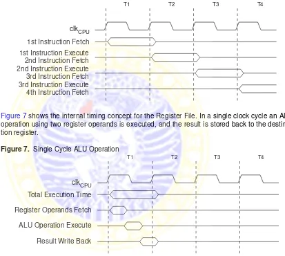
Figure 6 shows the parallel instruction fetches and instruction executions enabled by the Har-vard architecture and the fast-access Register File concept. This is the basic pipelining concept to obtain up to 1 MIPS per MHz with the corresponding unique results for functions per cost, functions per clocks, and functions per power-unit.
Figure 6. The Parallel Instruction Fetches and Instruction Executions
Figure 7 shows the internal timing concept for the Register File. In a single clock cycle an ALU operation using two register operands is executed, and the result is stored back to the destina-tion register.
Figure 7. Single Cycle ALU Operation
Reset and
Interrupt Handling
The AVR provides several different interrupt sources. These interrupts and the separate reset vector each have a separate program vector in the program memory space. All interrupts are assigned individual enable bits which must be written logic one together with the Global Interrupt Enable bit in the Status Register in order to enable the interrupt. Depending on the Program Counter value, interrupts may be automatically disabled when Boot Lock bits BLB02 or BLB12 are programmed. This feature improves software security. See the section “Memory Program-ming” on page 259 for details.
The lowest addresses in the program memory space are by default defined as the Reset and Interrupt Vectors. The complete list of vectors is shown in “Interrupts” on page 45. The list also determines the priority levels of the different interrupts. The lower the address the higher is the priority level. RESET has the highest priority, and next is INT0 – the External Interrupt Request
clk
1st Instruction Fetch 1st Instruction Execute 2nd Instruction Fetch 2nd Instruction Execute 3rd Instruction Fetch 3rd Instruction Execute 4th Instruction Fetch
T1 T2 T3 T4
CPU
Total Execution Time
Register Operands Fetch
ALU Operation Execute
Result Write Back
T1 T2 T3 T4