SECOND EDITION
Alexander Miczo
A JOHN WILEY & SONS, INC., PUBLICATION
Published by John Wiley & Sons, Inc., Hoboken, New Jersey. Published simultaneously in Canada.
No part of this publication may be reproduced, stored in a retrieval system, or transmitted in any form or by any means, electronic, mechanical, photocopying, recording, scanning, or otherwise, except as permitted under Section 107 or 108 of the 1976 United States Copyright Act, without either the prior written permission of the Publisher, or authorization through payment of the appropriate per-copy fee to the Copyright Clearance Center, Inc., 222 Rosewood Drive, Danvers, MA 01923, 978-750-8400, fax 978-750-4470, or on the web at
www.copyright.com. Requests to the Publisher for permission should be addressed to the Permissions Department, John Wiley & Sons, Inc., 111 River Street, Hoboken, NJ 07030, (201) 748-6011, fax (201) 748-6008, e-mail: [email protected].
Limit of Liability/Disclaimer of Warranty: While the publisher and author have used their best efforts in preparing this book, they make no representations or warranties with respect to the accuracy or completeness of the contents of this book and specifically disclaim any implied warranties of merchantability or fitness for a particular purpose. No warranty may be created or extended by sales representatives or written sales materials. The advice and strategies contained herein may not be suitable for your situation. You should consult with a professional where appropriate. Neither the publisher nor author shall be liable for any loss of profit or any other commercial damages, including but not limited to special, incidental, consequential, or other damages.
For general information on our other products and services please contact our Customer Care Department within the U.S. at 877-762-2974, outside the U.S. at 317-572-3993 or
fax 317-572-4002.
Wiley also publishes its books in a variety of electronic formats. Some content that appears in print, however, may not be available in electronic format.
Library of Congress Cataloging-in-Publication Data: Miczo, Alexander.
Digital logic testing and simulation / Alexander Miczo—2nd ed. p. cm.
Rev. ed. of: Digital logic testing and simulation. c1986. Includes bibliographical references and index. ISBN 0-471-43995-9 (cloth)
1. Digital electronics—Testing. I. Miczo, Alexander. Digital logic testing and simulation II. Title.
TK7868.D5M49 2003 621.3815′48—dc21
2003041100
Printed in the United States of America
v
CONTENTS
Preface xvii
1 Introduction 1
1.1 Introduction 1
1.2 Quality 2
1.3 The Test 2
1.4 The Design Process 6
1.5 Design Automation 9
1.6 Estimating Yield 11
1.7 Measuring Test Effectiveness 14
1.8 The Economics of Test 20
1.9 Case Studies 23
1.9.1 The Effectiveness of Fault Simulation 23 1.9.2 Evaluating Test Decisions 24 1.10 Summary 26
Problems 29
References 30
2 Simulation 33
2.1 Introduction 33
2.2 Background 33
2.3 The Simulation Hierarchy 36
2.4 The Logic Symbols 37
2.5 Sequential Circuit Behavior 39
2.6 The Compiled Simulator 44
2.6.2 Sequential Circuit Simulation 48
2.6.3 Timing Considerations 50
2.6.4 Hazards 50
2.6.5 Hazard Detection 52
2.7 Event-Driven Simulation 54
2.7.1 Zero-Delay Simulation 56
2.7.2 Unit-Delay Simulation 58
2.7.3 Nominal-Delay Simulation 59
2.8 Multiple-Valued Simulation 61
2.9 Implementing the Nominal-Delay Simulator 64
2.9.1 The Scheduler 64
2.9.2 The Descriptor Cell 67
2.9.3 Evaluation Techniques 70
2.9.4 Race Detection in Nominal-Delay Simulation 71
2.9.5 Min–Max Timing 72
2.10 Switch-Level Simulation 74
2.11 Binary Decision Diagrams 86
2.11.1 Introduction 86
2.11.2 The Reduce Operation 91
2.11.3 The Apply Operation 96
2.12 Cycle Simulation 101
2.13 Timing Verification 106
2.13.1 Path Enumeration 107
2.13.2 Block-Oriented Analysis 108 2.14 Summary 110
Problems 111
References 116
3 Fault Simulation 119
3.1 Introduction 119
3.2 Approaches to Testing 120
3.3 Analysis of a Faulted Circuit 122 3.3.1 Analysis at the Component Level 122
3.3.2 Gate-Level Symbols 124
CONTENTS vii
3.4 The Stuck-At Fault Model 125
3.4.1 The AND Gate Fault Model 127 3.4.2 The OR Gate Fault Model 128 3.4.3 The Inverter Fault Model 128 3.4.4 The Tri-State Fault Model 128 3.4.5 Fault Equivalence and Dominance 129 3.5 The Fault Simulator: An Overview 131
3.6 Parallel Fault Processing 134
3.6.1 Parallel Fault Simulation 134 3.6.2 Performance Enhancements 136 3.6.3 Parallel Pattern Single Fault Propagation 137 3.7 Concurrent Fault Simulation 139 3.7.1 An Example of Concurrent Simulation 139 3.7.2 The Concurrent Fault Simulation Algorithm 141 3.7.3 Concurrent Fault Simulation: Further Considerations 146
3.8 Delay Fault Simulation 147
3.9 Differential Fault Simulation 149 3.10 Deductive Fault Simulation 151 3.11 Statistical Fault Analysis 152 3.12 Fault Simulation Performance 155 3.13 Summary 157
Problems 159
References 162
4 Automatic Test Pattern Generation 165
4.1 Introduction 165
4.2 The Sensitized Path 165
4.2.1 The Sensitized Path: An Example 166 4.2.2 Analysis of the Sensitized Path Method 168
4.3 The D-Algorithm 170
4.3.1 The D-Algorithm: An Analysis 171 4.3.2 The Primitive D-Cubes of Failure 174
4.3.3 Propagation D-Cubes 177
4.3.4 Justification and Implication 179
4.4 Testdetect 182 4.5 The Subscripted D-Algorithm 184
4.6 PODEM 188
4.7 FAN 193
4.8 Socrates 202
4.9 The Critical Path 205
4.10 Critical Path Tracing 208
4.11 Boolean Differences 210
4.12 Boolean Satisfiability 216
4.13 Using BDDs for ATPG 219
4.13.1 The BDD XOR Operation 219
4.13.2 Faulting the BDD Graph 220 4.14 Summary 224
Problems 226
References 230
5 Sequential Logic Test 233
5.1 Introduction 233
5.2 Test Problems Caused by Sequential Logic 233
5.2.1 The Effects of Memory 234
5.2.2 Timing Considerations 237
5.3 Sequential Test Methods 239
5.3.1 Seshu’s Heuristics 239
5.3.2 The Iterative Test Generator 241
5.3.3 The 9-Value ITG 246
5.3.4 The Critical Path 249
5.3.5 Extended Backtrace 250
CONTENTS ix
5.7 Summary 277
Problems 278
References 280
6 Automatic Test Equipment 283
6.1 Introduction 283
6.2 Basic Tester Architectures 284
6.2.1 The Static Tester 284
6.2.2 The Dynamic Tester 286
6.3 The Standard Test Interface Language 288
6.4 Using the Tester 293
6.5 The Electron Beam Probe 299
6.6 Manufacturing Test 301
6.7 Developing a Board Test Strategy 304
6.8 The In-Circuit Tester 307
6.9 The PCB Tester 310
6.9.1 Emulating the Tester 311
6.9.2 The Reference Tester 312
6.9.3 Diagnostic Tools 313
6.10 The Test Plan 315
6.11 Visual Inspection 316
6.12 Test Cost 319
6.13 Summary 319
Problems 320
References 321
7 Developing a Test Strategy 323
7.1 Introduction 323
7.2 The Test Triad 323
7.3 Overview of the Design and Test Process 325
7.4 A Testbench 327
7.5 Fault Modeling 331
7.5.1 Checkpoint Faults 331
7.5.2 Delay Faults 333
7.5.3 Redundant Faults 334
7.5.4 Bridging Faults 335
7.5.5 Manufacturing Faults 337
7.6 Technology-Related Faults 337
7.6.1 MOS 338
7.6.2 CMOS 338
7.6.3 Fault Coverage Results in Equivalent Circuits 340
7.7 The Fault Simulator 341
7.7.1 Random Patterns 342
7.7.2 Seed Vectors 343
7.7.3 Fault Sampling 346
7.7.4 Fault-List Partitioning 347 7.7.5 Distributed Fault Simulation 348 7.7.6 Iterative Fault Simulation 348 7.7.7 Incremental Fault Simulation 349
7.7.8 Circuit Initialization 349
7.7.9 Fault Coverage Profiles 350
7.7.10 Fault Dictionaries 351
7.7.11 Fault Dropping 352
7.8 Behavioral Fault Modeling 353
7.8.1 Behavioral MUX 354
7.8.2 Algorithmic Test Development 356 7.8.3 Behavioral Fault Simulation 361
7.8.4 Toggle Coverage 364
7.8.5 Code Coverage 365
7.9 The Test Pattern Generator 368
7.9.1 Trapped Faults 368
7.9.2 SOFTG 369
7.9.3 The Imply Operation 369
7.9.4 Comprehension Versus Resolution 371 7.9.5 Probable Detected Faults 372 7.9.6 Test Pattern Compaction 372
7.9.7 Test Counting 374
CONTENTS xi
7.10.2 ATPG User Controls 380
7.10.3 Fault-List Management 381
7.11 Summary 382
Problems 383
References 385
8 Design-For-Testability 387
8.1 Introduction 387
8.2 Ad Hoc Design-for-Testability Rules 388 8.2.1 Some Testability Problems 389
8.2.2 Some Ad Hoc Solutions 393
8.3 Controllability/Observability Analysis 396
8.3.1 SCOAP 396
8.3.2 Other Testability Measures 403 8.3.3 Test Measure Effectiveness 405 8.3.4 Using the Test Pattern Generator 406
8.4 The Scan Path 407
8.4.1 Overview 407
8.4.2 Types of Scan-Flops 410
8.4.3 Level-Sensitive Scan Design 412
8.4.4 Scan Compliance 416
8.4.5 Scan-Testing Circuits with Memory 418
8.4.6 Implementing Scan Path 420
8.5 The Partial Scan Path 426
8.6 Scan Solutions for PCBs 432
8.6.1 The NAND Tree 433
8.6.2 The 1149.1 Boundary Scan 434
8.7 Summary 443
Problems 444
References 449
9 Built-In Self-Test 451
9.1 Introduction 451
9.2 Benefits of BIST 452
9.3.1 A Mathematical Basis for Self-Test 455
9.3.2 Implementing the LFSR 459
9.3.3 The Multiple Input Signature Register (MISR) 460
9.3.4 The BILBO 463
9.4 Random Pattern Effectiveness 464
9.4.1 Determining Coverage 464
9.4.2 Circuit Partitioning 465
9.4.3 Weighted Random Patterns 467
9.4.4 Aliasing 470
9.4.5 Some BIST Results 471
9.5 Self-Test Applications 471
9.5.1 Microprocessor-Based Signature Analysis 471 9.5.2 Self-Test Using MISR/Parallel SRSG (STUMPS) 474 9.5.3 STUMPS in the ES/9000 System 477 9.5.4 STUMPS in the S/390 Microprocessor 478
9.5.5 The Macrolan Chip 480
9.5.6 Partial BIST 482
9.6 Remote Test 484
9.6.1 The Test Controller 484
9.6.2 The Desktop Management Interface 487
9.7 Black-Box Testing 488
9.7.1 The Ordering Relation 489
9.7.2 The Microprocessor Matrix 493
9.7.3 Graph Methods 494
9.8 Fault Tolerance 495
9.8.1 Performance Monitoring 496
9.8.2 Self-Checking Circuits 498
9.8.3 Burst Error Correction 499
9.8.4 Triple Modular Redundancy 503 9.8.5 Software Implemented Fault Tolerance 505
9.9 Summary 505
Problems 507
References 510
10 Memory Test 513
CONTENTS xiii 10.2 Semiconductor Memory Organization 514
10.3 Memory Test Patterns 517
10.4 Memory Faults 521
10.5 Memory Self-Test 524
10.5.1 A GALPAT Implementation 525 10.5.2 The 9N and 13N Algorithms 529
10.5.3 Self-Test for BIST 531
10.5.4 Parallel Test for Memories 531
10.5.5 Weak Read–Write 533
10.6 Repairable Memories 535
10.7 Error Correcting Codes 537
10.7.1 Vector Spaces 538
10.7.2 The Hamming Codes 540
10.7.3 ECC Implementation 542
10.7.4 Reliability Improvements 543
10.7.5 Iterated Codes 545
10.8 Summary 546
Problems 547
References 549
11 IDDQ 551
11.1 Introduction 551 11.2 Background 551
11.3 Selecting Vectors 553
11.3.1 Toggle Count 553
11.3.2 The Quietest Method 554
11.4 Choosing a Threshold 556
11.5 Measuring Current 557
11.6 IDDQ Versus Burn-In 559
11.7 Problems with Large Circuits 562 11.8 Summary 564
Problems 565
12 Behavioral Test and Verification 567
12.1 Introduction 567 12.2 Design Verification: An Overview 568 12.3 Simulation 570 12.3.1 Performance Enhancements 570 12.3.2 HDL Extensions and C++ 572 12.3.3 Co-design and Co-verification 573 12.4 Measuring Simulation Thoroughness 575
12.4.1 Coverage Evaluation 575
12.4.2 Design Error Modeling 578
12.5 Random Stimulus Generation 581
12.6 The Behavioral ATPG 587
12.6.1 Overview 587
12.6.2 The RTL Circuit Image 588
12.6.3 The Library of Parameterized Modules 589 12.6.4 Some Basic Behavioral Processing Algorithms 593 12.7 The Sequential Circuit Test Search System (SCIRTSS) 597 12.7.1 A State Traversal Problem 597
12.7.2 The Petri Net 602
12.8 The Test Design Expert 607
12.8.1 An Overview of TDX 607
12.8.2 DEPOT 614
12.8.3 The Fault Simulator 616
12.8.4 Building Goal Trees 617
12.8.5 Sequential Conflicts in Goal Trees 618 12.8.6 Goal Processing for a Microprocessor 620 12.8.7 Bidirectional Goal Search 624 12.8.8 Constraint Propagation 625 12.8.9 Pitfalls When Building Goal Trees 626 12.8.10 MaxGoal Versus MinGoal 627
12.8.11 Functional Walk 629
12.8.12 Learn Mode 630
12.8.13 DFT in TDX 633
12.9 Design Verification 635
12.9.1 Formal Verification 636
CONTENTS xv
12.9.3 Equivalence Checking 638
12.9.4 Model Checking 640
12.9.5 Symbolic Simulation 648
12.10 Summary 650
Problems 652
References 653
xvii
PREFACE
About one and a half decades ago the state of the art in DRAMs was 64K bytes, a typical personal computer (PC) was implemented with about 60 to 100 dual in-line packages (DIPs), and the VAX11/780 was a favorite platform for electronic design automation (EDA) developers. It delivered computational power rated at about one MIP (million instructions per second), and several users frequently shared this machine through VT100 terminals.
Now, CPU performance and DRAM capacity have increased by more than three orders of magnitude. The venerable VAX11/780, once a benchmark for performance comparison and host for virtually all EDA programs, has been relegated to muse-ums, replaced by vastly more powerful PCs, implemented with fewer than a half dozen integrated circuits (ICs), at a fraction of the cost. Experts predict that shrink-ing geometries, and resultant increase in performance, will continue for at least another 10 to 15 years.
Already, it is becoming a challenge to use the available real estate on a die. Whereas in the original Pentium design various teams vied for a few hundred addi-tional transistors on the die,1 it is now becoming increasingly difficult for a design team to use all of the available transistors.2
The ubiquitous 8-bit microcontroller appears in entertainment products and in automobiles; billions are sold each year. Gordon Moore, Chairman Emeritus of Intel Corp., observed that these less glamorous workhorses account for more than 98% of Intel’s unit sales.3 More complex ICs perform computation, control, and communi-cations in myriad applicommuni-cations. With contemporary EDA tools, one logic designer can create complex digital designs that formerly required a team of a half dozen logic designers or more. These tools place logic design capability into the hands of an ever-growing number of users. Meanwhile, these development tools themselves continue to evolve, reducing turn-around time from design of logic circuit to receipt of fabricated parts.
The increase in size and complexity of circuits on a chip, often with little or no increase in the number of I/O pins, creates a testing bottleneck. Much more logic must be controlled and observed with the same number of I/O pins, making it more difficult to test the chip. Yet, the need for testing continues to grow in importance. The test must detect failures in individual units, as well as failures caused by defec-tive manufacturing processes. Random defects in individual units may not signifi-cantly impact a company’s balance sheet, but a defective manufacturing process for a complex circuit, or a design error in some obscure function, could escape detec-tion until well after first customer shipments, resulting in a very expensive product recall.
Public safety must also be taken into account. Digital logic devices have become pervasive in products that affect public safety, including applications such as trans-portation and human implants. These products must be thoroughly tested to ensure that they are designed and fabricated correctly. Where design and test shared tools in the past, there is a steadily growing divergence in their methodologies. Formal veri-fication techniques are emerging, and they are of particular importance in applica-tions involving public safety.
Each new generation of EDA tools makes it possible to design and fabricate chips of greater complexity at lower cost. As a result, testing consumes a greater percent-age of total production cost. It requires more effort to create a test program and requires more stimuli to exercise the chip. The difficulty in creating test programs for new designs also contributes to delays in getting products to the marketplace. Product managers must balance the consequences of delaying shipment of a product for which adequate test programs have not yet been developed against the conse-quences of shipping product and facing the prospect of wholesale failure and return of large quantities of defective products.
New test strategies are emerging in response to test problems arising from these increasingly complex devices, and greater emphasis is placed on finding defects as early as possible in the manufacturing cycle. New algorithms are being devised to create tests for logic circuits, and more attention is being given to design-for-test (DFT) techniques that require participation by logic designers, who are being asked to adhere to design rules that facilitate design of more testable circuits.
Built-in self-test (BIST) is a logical extension of DFT. It embeds test mechanisms directly into the product being designed, often using DFT structures. The goal is to place stimulus generation and response evaluation circuits closer to the logic being tested.
PREFACE xix Remote diagnostics are yet another strategy employed in the quest for reliable computing. Some manufacturers of personal computers provide built-in diagnostics. If problems occur during operation and if the problem does not interfere with the ability to communicate via the modem, then the computer can dial a remote com-puter that is capable of analyzing and diagnosing the cause of the problem.
It should be obvious from the preceding paragraphs that there is no single solu-tion to the test problem. There are many solusolu-tions, and a solusolu-tion may be appropri-ate for one application but not for another. Furthermore, the best solution for a particular application may be a combination of available solutions. This requires that designers and test engineers understand the strengths and weaknesses of the various approaches.
THE ROADMAP
This textbook contains 12 chapters. The first six chapters can be viewed as building blocks. Topics covered include simulation, fault simulation, combinational and sequential test pattern generation, and a brief introduction to tester architectures. The last six chapters build on the first six. They cover design-for-test (DFT), built-in self-test (BIST), fault tolerance, memory test, IDDQ test, and, finally, behavioral test and verification. This dichotomy represents a natural partition for a two-semester course. Some examples make use of the Verilog hardware design language (HDL). For those readers who do not have access to a commercial Verilog product, a quite good (and free) Verilog compiler/simulator can be downloaded from http:// www.icarus.com. Every effort was made to avoid relying on advanced HDL con-cepts, so that the student familiar only with programming languages, such as C, can follow the Verilog examples.
PART I
Chapter 1 begins with some general observations about design, test, and quality. Acceptable quality level (AQL) depends both on the yield of the manufacturing pro-cesses and on the thoroughness of the test programs that are used to identify defec-tive product. Process yield and test thoroughness are focal points for companies trying to balance quality, product cost, and time to market in order to remain profit-able in a highly competitive industry.
represents one end of the simulation spectrum. Behavioral simulation and cycle simulation represent the other end. Binary decision diagrams (BDDs), used in support of cycle simulation, are introduced in this chapter. Timing analysis in syn-chronous designs is also discussed.
Chapter 3 concentrates on fault simulation algorithms, including parallel, deductive, and concurrent fault simulation. The chapter begins with a discussion of fault modeling, including, of course, the stuck-at fault model. The basic algorithms are examined, with a look at ways in which excess computations can be squeezed out of the algorithms in order to improve performance. The relationship between algorithms and the design environment is also examined: For example, how are the different algorithms affected by the choice of synchronous or asynchronous design environment?
The topic for Chapter 4 is automatic test pattern generation (ATPG) for combi-national circuits. Topological, or path tracing, methods, including the D-algorithm with its formal notation, along with PODEM, FAN, and the critical path, are examined. The subscripted D-algorithm is examined; it represents an example of symbolic propagation. Algebraic methods are described next; these include Bool-ean difference and BoolBool-ean satisfiability. Finally, the use of BDDs for ATPG is discussed.
Sequential ATPG merits a chapter of its own. The search for an effective sequential ATPG has continued unabated for over a quarter-century. The problem is complicated by the presence of memory, races, and hazards. Chapter 5 focuses on some of the methods that have evolved to deal with sequential circuits, including the iterative test generator (ITG), the 9-value ITG, and the extended backtrace (EBT). We also look at some experiments on state machines, including homing sequences, distinguishing sequences, and so on, and see how these lead to circuits which, although testable, require more information than is available from the netlist.
Chapter 6 focuses on automatic test equipment. Testers in use today are extraor-dinarily complex; they have to be in order to keep up with the ICs and PCBs in pro-duction; hence this chapter can be little more than a brief overview of the subject. Testers are used to test circuits in production environments, but they are also used to characterize ICs and PCBs. In order to perform characterization, the tester must be able to operate fast enough to clock the circuit at its intended speed, it must be able to accurately measure current and voltage, and it must be possible to switch input levels and strobe output pins in a matter of picoseconds. The Standard Test Interface Language (STIL) is also examined in this chapter. Its goal it to give a uniform appearance to the many different tester architectures on the marketplace.
PART II
PREFACE xxi and in conjunction with other tools, in order to create a successful test strategy. This often requires an understanding of the environment in which they function, includ-ing such thinclud-ings as design methodologies, HDLs, circuit models, data structures, and fault modeling strategies. Different technologies and methodologies require very different tools.
The focus up to this point has been on the traditional approach to test—that is, apply stimuli and measure response at the output pins. Unfortunately, existing algorithms, despite decades of research, remain ineffective for general sequential logic. If the algorithms cannot be made powerful enough to test sequential logic, then circuit complexity must be reduced in order to make it testable. Chapters 8 and 9 look at ways to improve testability by altering the design in order to improve access to its inner workings. The objectives are to make it easier to apply a test (improve controllability) and make it easier to observe test results (improve observability). Design-for-test (DFT) makes it easier to develop and apply tests via conventional testers. Built-in self-test (BIST) attempts to replace the tester, or at least offload many of its tasks. Both methodologies make testing easier by reducing the amount and/or complexity of logic through which a test must travel either to stimulate the logic being tested or to reach an observable output whereby the test can be monitored.
Memory test is covered in Chapter 10. These structures have their own problems and solutions as a result of their regular, repetitive structure and we examine some algorithms designed to exploit this regularity. Because memories keep growing in size, the memory test problem continues to escalate. The problem is further exac-erbated by the fact that increasingly larger memories are being embedded in microprocessors and other devices. In fact, it has been suggested that as micropro-cessors grow in transistor count, they are becoming de facto memories with a little logic wrapped around them. A growing trend in memories is the use of memory BIST (MBIST). This chapter contains two Verilog implementations of memory test algorithms.
Complementary metal oxide semiconductor (CMOS) circuits draw little or no current except when clocked. Consequently, excessive current observed when an IC is in the quiescent state is indicative of either a hard failure or a potential reliability problem. A growing number of investigators have researched the implications of this observation, and determined how to leverage this potentially powerful test strategy. IDDQ will be the focus of Chapter 11.
The goal of this textbook is to cover a representative sample of algorithms and practices used in the IC industry to identify faulty product and prevent, to the extent possible, tester escapes—that is, faulty devices that slip through the test process and make their way into the hands of customers. However, digital test is not a “one size fits all” industry.
Given two companies with similar digital products, test practices may be as dif-ferent as day and night, and yet both companies may have rational test plans. Minor nuances in product manufacturing practices can dictate very different strategies. Choices must be made everywhere in the design and test cycle. Different individuals within the same project may be using simulators ranging from switch-level to cycle-based. Testability enhancements may range from ad hoc techniques, to partial-scan, to full-scan. Choices will be dictated by economics, the capabilities of the available tools, the skills of the design team, and other circumstances.
One of the frustrations faced over the years by those responsible for product qual-ity has been the reluctance on the part of product planners to face up to and address test issues. Nearly 500 years ago Nicolo Machiavelli, in his book The Prince, observed that “fevers, as doctors say, at their beginning are easy to cure but difficult to recognise, but in course of time when they have not at first been recognised, and treated, become easy to recognise and difficult to cure.5” In a similar vein, in the early stages of a design, test problems are difficult to recognize but easy to solve; further into the process, test problems become easier to recognize but more difficult to cure.
REFERENCES
1. Brandt, R., The Birth of Intel’s Pentium Chip—and the Labor Pains, Business Week, March 29, 1993, pp. 94–95.
2. Bass, Michael J., and Clayton M. Christensen, The Future of the Microprocessor Business,
IEEE Spectrum, Vol. 39, No. 4, April 2002, pp. 34–39.
3. Port, O., Gordon Moore’s Crystal Ball, Business Week, June 23, 1997, p. 120.
4. Foderaro, J. K., K. S. Van Dyke, and D. A. Patterson, Running RISCs, VLSI Des., September–October 1982, pp. 27–32.
1
Digital Logic Testing and Simulation, Second Edition, by Alexander Miczo ISBN 0-471-43995-9 Copyright © 2003 John Wiley & Sons, Inc.
CHAPTER 1
Introduction
1.1 INTRODUCTION
Things don’t always work as intended. Some devices are manufactured incorrectly, others break or wear out after extensive use. In order to determine if a device was manufactured correctly, or if it continues to function as intended, it must be tested. The test is an evaluation based on a set of requirements. Depending on the complex-ity of the product, the test may be a mere perusal of the product to determine whether it suits one’s personal whims, or it could be a long, exhaustive checkout of a complex system to ensure compliance with many performance and safety criteria. Emphasis may be on speed of performance, accuracy, or reliability.
Consider the automobile. One purchaser may be concerned simply with color and styling, another may be concerned with how fast the automobile accelerates, yet another may be concerned solely with reliability records. The automobile manufac-turer must be concerned with two kinds of test. First, the design itself must be tested for factors such as performance, reliability, and serviceability. Second, individual units must be tested to ensure that they comply with design specifications.
Testing will be considered within the context of digital logic. The focus will be on technical issues, but it is important not to lose sight of the economic aspects of the problem. Both the cost of developing tests and the cost of applying tests to individual units will be considered. In some cases it becomes necessary to make trade-offs. For example, some algorithms for testing memories are easy to create; a computer pro-gram to generate test vectors can be written in less than 12 hours. However, the set of test vectors thus created may require several millenia to apply to an actual device. Such a test is of no practical value. It becomes necessary to invest more effort into initially creating a test in order to reduce the cost of applying it to individual units.
2 INTRODUCTION
assemblies can be better appreciated when viewed within the context of the overall design process. Within this process we note design stages where testing is required. We then look at design aids that have evolved over the years for designing and testing digital devices. Finally, we examine the economics of testing.
1.2 QUALITY
Quality frequently surfaces as a topic for discussion in trade journals and periodi-cals. However, it is seldom defined. Rather, it is assumed that the target audience understands the intended meaning in some intuitive way. Unfortunately, intuition can lead to ambiguity or confusion. Consider the previously mentioned automobile. For a prospective buyer it may be deemed to possess quality simply because it has a soft leather interior and an attractive appearance. This concept of quality is clearly subjective: It is based on individual expectations. But expectations are fickle: They may change over time, sometimes going up, sometimes going down. Furthermore, two customers may have entirely different expectations; hence this notion of quality does not form the basis for a rigorous definition.
In order to measure quality quantitatively, a more objective definition is needed. We choose to define quality as the degree to which a product meets its requirements. More precisely, it is the degree to which a device conforms to applicable specifica-tions and workmanship standards.1 In an integrated circuit (IC) manufacturing envi-ronment, such as a wafer fab area, quality is the absence of “drift”—that is, the absence of deviation from product specifications in the production process. For digi-tal devices the following equation, which will be examined in more detail in a later section, is frequently used to quantify quality level:2
AQL = Y( 1 −T) (1.1) In this equation, AQL denotes acceptable quality level, it is a function of Y (product yield) and T (test thoroughness). If no testing is done, AQL is simply the yield—that is, the number of good devices divided by the total number of devices made. Con-versely, if a complete test were created, then T = 1, and all defects are detected so no bad devices are shipped to the customer.
Equation (1.1) tells us that high quality can be realized by improving product yield and/or the thoroughness of the test. In fact, if Y ≥ AQL, testing is not required. That is rarely the case, however. In the IC industry a high yield is often an indication that the process is not aggressive enough. It may be more economically rewarding to shrink the geometry, produce more devices, and screen out the defective devices through testing.
1.3 THE TEST
THE TEST 3 Figure 1.1 depicts a test configuration in which stimuli are applied to a device-under-test (DUT), and the response is evaluated. If we know what the expected response is from the correctly operating device, we can compare it to the response of the DUT to determine if the DUT is responding correctly.
When the DUT is a digital logic device, the stimuli are called test patterns or test vectors. In this context a vector is an ordered n-tuple; each bit of the vector is applied to a specific input pin of the DUT. The expected or predicted outcome is usually observed at output pins of the device, although some test configurations per-mit monitoring of test points within the circuit that are not normally accessible dur-ing operation. A tester captures the response at the output pins and compares that response to the expected response determined by applying the stimuli to a known good device and recording the response, or by creating a model of the circuit (i.e., a representation or abstraction of selected features of the system3) and simulating the input stimuli by means of that model. If the DUT response differs from the expected response, then an error is said to have occurred. The error results from a defect in the circuit.
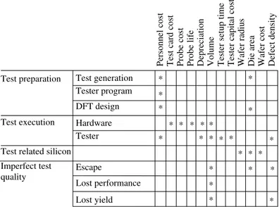
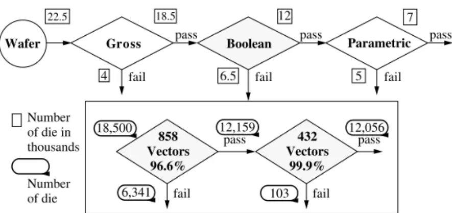
The next step in the process depends on the type of test that is to be applied. A taxonomy of test types4 is shown in Table 1.1. The classifications range from testing die on a bare wafer to tests developed by the designer to verify that the design is cor-rect. In a typical manufacturing environment, where tests are applied to die on a wafer, the most likely response to a failure indication is to halt the test immediately and discard the failing part. This is commonly referred to as a go–nogo test. The object is to identify failing parts as quickly as possible in order to reduce the amount of time spent on the tester.
If several functional test programs were developed for the part, a common prac-tice is to arrange them so that the most effective test program—that is, the one that uncovers the most defective parts—is run first. Ranking the effectiveness of the test programs can be done through the use of a fault simulator, as will be explained in a subsequent chapter. The die that pass the wafer test are packaged and then retested. Bonding a chip to a package has the potential to introduce additional defects into the process, and these must be identified.
Binning is the practice of classifying chips according to the fastest speed at which they can operate. Some chips, such as microprocessors, are priced according to their clock speed. A chip with a 10% performance advantage may bring a 20–50% premium in the marketplace. As a result, chips are likely to first be tested at their maximum rated speed. Those that fail are retested at lower clock speeds until either they pass the test or it is determined that they are truly defective. It is, of course, pos-sible that a chip may run successfully at a clock speed lower than any for which it was tested. However, such chips can be presumed to have no market value.
Figure 1.1 Typical test configuration.
DUT
Stimulus
4 INTRODUCTION
Diagnosis may be called for when there is a yield crash—that is, a sudden, signif-icant drop in the number of devices that pass a test. To aid in investigating the causes, it may be necessary to create additional test vectors specifically for the pur-pose of isolating the source of the crash. For ICs it may be necessary to resort to an e-beam probe to identify the source. Production diagnostic tests are more likely to be created for a printed circuit board (PCB), since they are often repairable and gen-erally represent a larger manufacturing cost. Tests for memory arrays are thorough and methodical, thus serving both as go–no-go tests and as diagnostic tests. These tests permit substitution of spare rows or columns in order to repair the memory array, thereby significantly improving the yield.
Products tend to be more susceptible to yield problems in the early stages of their existence, since manufacturing processes are new and unfamiliar to employees. As a result, there are likely to be more occasions when it is necessary to investigate prob-lems in order to diagnose causes. For mature products, yield is frequently quite high, and testing may consist of sampling by randomly selecting parts for test. This is also a reasonable strategy for low complexity parts, such as a chip that goes into a wristwatch.
To protect against yield problems, particularly in the early phases of a project, burn-in is commonly employed. Burn-in stresses semiconductor products in order to
TABLE 1.1 Types of Tests
Type of Test Purpose of Test
Production
Wafer Sort or Probe Final or Package
Test of manufactured parts to sort out those that are faulty Test of each die on the wafer.
Test of packaged chips and separation into bins (mili-tary, commercial, industrial).
Acceptance Test to demonstrate the degree of compliance of a device with purchaser’s requirements.
Sample Test of some but not all parts.
Go–nogo Test to determine whether device meets specifications. Characterization or
engineering
Test to determine actual values of AC and DC parameters and the interaction of parameters. Used to set final specifications and to identify areas to improve pro-cess to increase yield.
Stress screening (burn-in) Test with stress (high temperature, temperature cycling, vibration, etc.) applied to eliminate short life parts. Reliability (accelerated
life)
Test after subjecting the part to extended high temperature to estimate time to failure in normal operation. Diagnostic (repair) Test to locate failure site on failed part.
Quality Test by quality assurance department of a sample of each lot of manufactured parts. More stringent than final test.
THE TEST 5 identify and eliminate marginal performers. The goal is to ensure the shipment of parts having an acceptably low failure rate and to potentially improve product reli-ability.5 Products are operated at environmental extremes, with the duration of this operation determined by product history. Manufacturers institute programs, such as Intel’s ZOBI (zero hour burn-in), for the purpose of eliminating burn-in and the resulting capital equipment costs.6
When stimuli are simulated against the circuit model, the simulator pro-duces a file that contains the input stimuli and expected response. This informa-tion goes to the tester, where the stimuli are applied to manufactured parts. However, this information does not provide any indication of just how effec-tive the test is at detecting defects internal to the circuit. Furthermore, if an erroneous response should occur at any of the output pins during testing of manufactured parts, there is no insight into the location of the defect that induced the incorrect response. Further testing may be necessary to distinguish which of several possible defects produced the response. This is accomplished through the use of fault models.
The process is essentially the same; that is, vectors are simulated against a model of the circuit, except that the computer model is modified to make it appear as though a fault were present. By simulating the correct model and the faulted model, responses from the two models can be compared. Furthermore, by injecting several faults into the model, one at a time, and then simulating, it is possible to compare the response of the DUT to that of the various faulted models in order to determine which faulted model either duplicates or most closely approximates the behavior of the DUT.
If the DUT responds correctly to all applied stimuli, confidence in the DUT increases. However, we cannot conclude that the device is fault-free! We can only conclude that it does not contain any of the faults for which it was tested, but it could contain other faults for which an effective test was not applied.
From the preceding paragraphs it can be seen that there are three major aspects of the test problem:
1. Specification of test stimuli 2. Determination of correct response
3. Evaluation of the effectiveness of the stimuli
Furthermore, this approach to testing can be used both to detect the presence of faults and to distinguish between several faults for repair purposes.
6 INTRODUCTION
ineffective stimuli will not uncover many defects. Hence, measuring the effective-ness of test stimuli, using an accepted metric, is another very important task.
1.4 THE DESIGN PROCESS
Table 1.1 identifies several types of tests, ranging from design verification, whose purpose is to ensure that a design conforms to the designer’s intent, to various kinds of tests directed toward identifying units with manufacturing defects, and tests whose purpose is to identify units that develop defects during normal usage. The goal during product design is to develop comprehensive test programs before a design is released to manufacturing. In reality, test programs are not always ade-quate and may have to be enhanced due to an excessive number of faulty units reaching end users. In order to put test issues into proper perspective, it will be helpful here to take a brief look at the design process, starting with initial product conception.
A digital device begins life as a concept whose eventual goal is to fill a perceived need. The concept may flow from an original idea or it may be the result of market research aimed at obtaining suggestions for enhancements to an existing product. Four distinct product development classifications have been identified:7
First of a kind Me too with a twist Derivative
Next-generation product
The “first of a kind” is a product that breaks new ground. Considerable innovation is required before it is implemented. The “me too with a twist” product adds incre-mental improvements to an existing product, perhaps a faster bus speed or a wider data path. The “derivative” is a product that is derived from an existing product. An example would be a product that adds functionality such as video graphics to a core microprocessor. Finally, the “next-generation product” replaces a mature product. A 64-bit microprocessor may subsume op-codes and basic capabilities, but also substantially improve on the performance and capabilities of its 32-bit predecessor.
THE DESIGN PROCESS 7
Figure 1.2 Design flow.
After a product has been defined and a decision has been made to manufacture and market the device, a number of activities must occur, as illustrated in Figure 1.2. These activities are shown as occurring sequentially, but frequently the activities overlap because, once a commitment to manufacture has been made, the objective is to get the product out the door and into the marketplace as quickly as possible. Obvi-ously, nothing happens until a development team is put in place. Sometimes the larg-est single factor influencing the time-to-market is the time required to allocate resources, including staff to implement the project and the necessary tools by which the staff can complete the design and put a manufacturing flow into place. For a device with a given level of performance, time of delivery will frequently determine if the product is competitive; that is, does it fall above or below the performance– time plot illustrated in Figure 1.3?
Once the behavioral specification has been completed, a functional design must be created. This is actually a continuous flow; that is, the behavior is identified, and then, based on available technology, architects identify functional units. At that stage of development an important decision must be made as to whether or not the product can meet the stated performance objectives, given the architecture and tech-nology to be used. If not, alternatives must be examined. During this phase the logic is partitioned into physical units and assigned to specific units such as chips, boards, or cabinets. The partitioning process attempts to minimize I/O pins and cabling between chips, boards, and units. Partitioning may also be used to advantage to sim-plify such things as test, component placement, and wire routing.
The use of hardware design languages (HDLs) for the design process has become virtually universal.Two popular HDLs, VHDL (VHSIC Hardware Description Lan-guage) and Verilog, are used to
Specify an architecture
Partition the architecture into smaller modules Synthesize an RTL description
Verify that a structural implementation corresponds to the architectural design Check out microcode and/or diagnostic programs
Serve as documentation
Figure 1.3 Performance–time plot.
Concept Behavioral design
RTL design
Logic design
Physical
design Mfg. Allocate
resources
Performance
Time Too late
8 INTRODUCTION
A behavioral description specifies what a design must do. There is usually little or no indication as to how it must be done. For example, a large case statement might identify operations to be performed by an ALU in response to different values applied to a control field. The RTL design refines the behavioral description. Opera-tions identified at the behavioral level are elaborated upon in more detail. RTL design is followed by logic design. This stage may be generated by synthesis pro-grams, or it may be created manually, or, more often, some modules are synthesized while others are manually designed or included from a library of predesigned mod-ules, some or all of which may have been purchased from an outside vendor. The use of predesigned, or core, modules may require selecting and/or altering components and specifying the interconnection of these components. At the end of the process, it may be the case that the design will not fit on a piece of silicon, or there may not be enough I/O pins to accommodate the signals, in which case it becomes necessary to reevaluate the design.
Physical design specifies the physical placement of components and the routing of wires between components. Placement may assign circuits to specific areas on a piece of silicon, it may specify the placement of chips on a PCB, or it may specify the assignment of PCBs to a cabinet. The routing task specifies the physical connec-tion of devices after they have been placed. In some applicaconnec-tions, only one or two connection layers are permitted. Other applications may permit PCBs with 20 or more interconnection layers, with alternating layers of metal interconnects and insu-lating material.
The final design is sent to manufacturing, where it is fabricated. Engineering changes must frequently be accommodated due to logic errors or other unexpected problems such as noise, timing, heat buildup, electrical interference, and so on, or inability to mass produce some critical parts.
In these various design stages there is a continuing need for testing. Require-ments analysis attempts to determine whether the product will fulfill its objectives, and testing techniques are frequently based on marketing studies. Early attempts to introduce more rigor into this phase included the use of design languages such as PSL/PSA (Problem Statement Language/Problem Statement Analyzer).8 It provided a way both to rigorously state the problem and to analyze the resulting design. PMS (Processors, Memories, Switches)9 was another early attempt to introduce rigor into the initial stages of a design project, permitting specification of a design via a set of consistent and systematic rules. It was often used to evaluate architec-tures at the system level, measuring data throughput and looking for design bottle-necks. Verilog and VHDL have become the standards for expressing designs at all levels of abstraction, although investigation into specification languages continues to be an active area of research. Its importance is seen from such statements as “requirements errors typically comprise over 40% of all errors in a software project”10 a n d “the really serious mistakes occur in the first day.”3
DESIGN AUTOMATION 9 chosen to confirm correctness of the design or to expose design errors. The design verification vectors must be sufficient to confirm that the design satisfies the behav-ior expressed in the product specification. Development of effective test stimuli at this state is highly iterative; a discrepancy between designer intent and simulation results often indicates the need for more stimuli to diagnose the underlying reason for the discrepancy. A growing trend at this level is the use of formal verification techniques (cf. Chapter 12.)
The logic design is tested in a manner similar to the functional design. A major difference is that the circuit description is more detailed; hence thorough analysis requires that simulations be more exhaustive. At the logic level, timing is of greater concern, and stimuli that were effective at the register transfer level (RTL) may not be effective in ferreting out critical timing problems. On the other hand, stimuli that produced correct or expected response from the RTL circuit may, when simulated by a timing simulator, indicate incorrect response or may indicate marginal perfor-mance, or the simulator may simply indicate that it cannot predict the correct response.
The testing of physical structure is probably the most formal test level. The test engineer works from a detailed design document to create tests that determine if response of the fabricated device corresponds to response of the design. Studies of fault behavior of the selected circuit family or technology permit the creation of fault models. These fault models are then used to create specific test stimuli that attempt to distinguish between the correctly operating device and a device with the fault.
This last category, which is the most highly developed of the design stages, due to its more formal and well-defined environment, is where we will concentrate our attention. However, many of the techniques that have been developed for structural testing can be applied to design verification at the logic and functional levels.
1.5 DESIGN AUTOMATION
Many of the activities performed by architects and logic designers were long ago recognized to be tedious, repetitious, error prone, and time-consuming, and hence could and should be automated. The mechanization of tedious design processes reduces the potential for errors caused by human fatigue, boredom, and inattention to mundane details. Early elimination of errors, which once was a desirable objec-tive, has now become a virtual necessity. The market window for new products is sometimes so small that much of that window will have evaporated in the time that it takes to correct an error and push the design through the entire fabrication cycle yet another time.
10 INTRODUCTION
automation (EDA). It does not replace the designer but, rather, enables the designer to be more productive and more creative. In addition, it provides access to IC design for many logic designers who know very little about the intricacies of laying out an IC design. It is one of the major factors responsible for taking cost out of digital products.
Depending on whether it is an IC, a PCB, or a system comprised of several PCBs, a typical EDA system supports some or all of the following capabilities:
Data management Record data Retrieve data Define relationships Perform rules checks Design analysis/verification
Evaluate performance/capabilities Simulate
Check timing Design fabrication
Perform placement and routing Create tests for structural defects Identify qualified vendors Documentation
Extract parts list
Create/update product specification
The data management system supports a data base that serves as a central repository for all design data. A data management program accepts data from the designer, for-mats it, and stores it in the data base. Some validity checks can be performed at this time to spot obvious errors. Programs must be able to retrieve specific records from the data base. Different applications require different records or combinations or records. As an example, one that we will elaborate on in a later chapter, a test pro-gram needs information concerning the specific ICs used in the design of a board, it needs information concerning their interconnections, and it needs information con-cerning their physical location on a board.
ESTIMATING YIELD 11 The data management system must be able to handle multiple revisions of a design or multiple physical implementations of a single architecture. This is true for manu-facturers who build a range of machines all of which implement the same architecture. It may not be necessary to maintain an architectural level copy with each physical implementation. The system must be able to control access and update to a design, both to protect proprietary design information from unauthorized disclosure and to protect the data base from inadvertent damage. A lock-out mechanism is useful to pre-vent simultaneous updates that could result in one or both of the updates being lost.
Design analysis and verification includes simulation of a design after it is recorded in the data base to verify that it is functionally correct. This may include RTL simulation using a hardware design language and/or simulation at a gate level with a logic simulator. Precise relationships must be satisfied between clock and data paths. After a logic board with many components is built, it is usually still pos-sible to alter the timing of critical paths by inserting delays on the board. On an IC there is no recourse but to redesign the chip. This evaluation of timing can be accomplished by simulating input vectors with a timing simulator, or it can be done by tracing specific paths and summing up the delays of elements along the way.
After a design has stabilized and has been entered into a data base, it can be fab-ricated. This involves placement either of chips on a board or of circuits on a die and then interconnecting them. This is usually accomplished by placement and routing programs. The process can be fully automated for simple devices, or for complex devices it may require an interactive process whereby computer programs do most of the task, but require the assistance of an engineer to complete the task. Checking programs are used after placement and routing.
Typical checks look for things such as runs too close to one another, and possible opens or shorts between runs. After placement and routing, other kinds of analysis can be performed. This includes such things as computing heat concentration on an IC or PCB and computing the reliability of an assembly based on the reliability of individual components and manufacturing processes. Testing the structure involves creation of test stimuli that can be applied to the manufactured IC or PCB to deter-mine if it has been fabricated correctly.
Documentation includes the extraction of parts lists, the creation of logic dia-grams and printing of RTL code. The parts list is used to maintain an inventory of parts in order to fabricate assemblies. The parts list may be compared against a mas-ter list that includes information such as preferred vendors, second sources, or almas-ter- alter-nate parts which may be used if the original part is unavailable. Preferred vendors may be selected based on an evaluation of their timeliness in delivering parts and the quality of parts received from them in the past. Logic diagrams are used by techni-cians and field engineers to debug faulty circuits as well as by the original designer or another designer who must modify or debug a logic design at some future date.
1.6 ESTIMATING YIELD
12 INTRODUCTION
situation in which a company was invited to submit a bid to manufacture a large CMOS custom logic chip. The chip had already been designed at another company and was to have a die area of 2.3 cm2. The company had experience making CMOS parts, but never one this large. Hence, they were uncertain as to how to estimate yield for a chip of this size.
When they extrapolated from existing data, using a computer-generated best-fit model, they obtained a yield estimate Y = 1.4%. Using a Poisson model with D0 = 2.1, where D0 is the average number of defects per unit area A, they obtained an estimate Y = 0.8%. They then calculated the yield using Seeds’ model,13 which gave Y = 17%. That was followed by Murphy’s model.14 It gave Y = 4%. They decided to average Seeds’ model and Murphy’s model and submit a bid based on 11% die sort yield. A year later they were producing chips with a yield of 6%, even though D0 had fallen from 2.1 to 1.9 defects/cm2. The company had started to evaluate the neg-ative binomial yield model Y = (1 + D0A/α)−α. A value of α = 3 produced a good fit for their yield data. Unfortunately, the company could not sustain losses on the prod-uct and dropped it from prodprod-uction, leaving the customer without a supply of parts.
Probability distribution functions are used to estimate the probability of an event occurring. The binomial probability distribution is a discrete distribution, which is expressed as
(1.2)
If P is the probability of a defect on a die, then P(k) is the probability of k defects on the die, when there are a total of n = D0Aw defects, where Aw is the area of the wafer. The probability P is D0A/D0Aw = A/Aw. Substituting into Eq. (1.2) yields
(1.3)
To derive the equation for a die with no defects, set k = 0. This yields
(1.4)
The first distribution that was frequently used to estimate yields was the Poisson distribution, which is expressed as
for k = 0, 1, 2, ... (1.5)
where λ0 is the average number of defects per die. For die with no defects (k = 0), the equation becomes . If λ0 = .5, the yield is predicted to be .607. In general, the Poisson distribution requires that defects be uniformly and randomly distributed. Hence, it tends to be pessimistic for larger die sizes. Considering again
ESTIMATING YIELD 13 the binomial distribution, if the number of trials, n, is large, and the probability p of occurrence of an event is close to zero, then the binomial distribution is closely approximated by the Poisson distribution with λ = n⋅p.
Another distribution commonly used to estimate yield is the normal distribution, also known as the Gaussian distribution. It is the familiar bell-shaped curve and is expressed as
(−∞ < k < ∞) (1.6)
The variable µ represents the mean, σ represents the standard deviation, and σ2 represents the variance. If n is large and if neither p or q is too close to zero, the binomial distribution can be closely approximated by a normal distribution. This can be expressed as
(1.7)
where np represents the mean for the binomial distribution, is the standard deviation, npq is the variance, and x is the number of successful trials.
When Murphy investigated the yield problem in 1964, he observed that defect and particle densities vary widely among chips, wafers, and runs. Under these cir-cumstances, the Poisson model is likely to underestimate yield, so he chose to use the normalized probability distribution function. To derive a yield equation, Murphy multiplied the probability distribution function with the probability p that the device was good, for a given defect density D, and then summed that over all values of D, that is,
(1.8)
He substituted for the probability that the device was good. However, he could not integrate the bell-shaped curve, so he approximated it with a triangle func-tion. This gave
(1.9)
By substituting other expressions for f(D) in Eq. (1.8), other yield equations result. Seeds used an exponential distribution function . Substituting this into Eq. (1.8), he obtained
(1.10)
In 1973 Charles Stapper15 derived a yield equation that is often referred to as a negative binomial distribution. By substituting and the gamma
distribution function into Murphy’s equation [Eq. (1.8)] and integrating, he obtained
(1.11) The mean of the gamma function is given by µ = α/λ, whereas the variance is given by α/λ2. Compare these with the mean and variance of the negative binomial distribution, sometimes referred to as Pascal’s distribution: mean = nq/p and variance = nq/p2.
The parameter α in Eq. (1.11) is referred to as the cluster parameter. By selecting appropriate values of α, the other yield equations can be approximated by Eq. (1.11). The value of α can be determined through statistical analysis of defect distribution data, permitting an accurate yield model to be obtained.
1.7 MEASURING TEST EFFECTIVENESS
In this chapter the intent has been to survey some of the many approaches to digital logic test. The objective is to illustrate how these approaches fit together to produce a program targeted toward product quality. Hence, we have touched only briefly on many topics that will be covered in greater detail in subsequent chapters. One of the topics examined here is fault modeling. It has been the practice, for over three decades, to resort to the use of stuck-at models to imitate the effects of defects. This model was more realistic when (small-scale integration) (SSI) was predominant. However, the stuck-at model, for practical reasons, is still widely used by commer-cial tools. Basically put, this model assumes that an input or output of a logic gate (e.g., an inverter, an AND gate, an OR gate, etc.) is stuck to a logic value 0 or 1 and is insensitive to signal changes from the signal that drives it.
With this faulting mechanism the process, in rather general terms, proceeds as follows: Computer models of digital circuits are created, and faults are injected into the model. The fault-free circuit and the faulted circuit are simulated. If there is a difference in response at an observable I/O pin, the fault is classified as detected. After many faults are evaluated in this manner, fault coverage is computed as
Fault coverage = No. faults detected / No.faults modeled
Given a fault coverage number, there are two questions that occur: How accurate is it, and for a given fault coverage, how many defective chips are likely to become tester escapes? Accuracy of fault coverage will depend on the faults selected and the accuracy of the fault model relative to real defect mechanisms. Fault selection requires a statistically meaningful random sample, although it is often the practice to
f( )λ 1 Γ( )βα α
---λα–1e–λ β⁄ =
MEASURING TEST EFFECTIVENESS 15 fault simulate a universal sample of faults, meaning faults applied to all logic ele-ments in a circuit. The fault model, like any model, is an imperfect replica. It is rather simplistic when compared to the various, complex kinds of defects that can occur in a circuit; therefore, predictions of test effectiveness based on the stuck-at model are prone to error and imprecision. The number of tester escapes will depend on the thoroughness of the test—that is, the fault coverage, the accuracy of that fault coverage, and the process yield.
The term defect level (DL) is used to denote the fraction of shipped ICs that are bad. It is computed as
DL = Number of faulty units shipped / Total no. units shipped (1.12)
It has also been variously referred to as field reject rate and reject ratio. In this sec-tion we adhere to the terminology used by the original authors in their derivasec-tions.
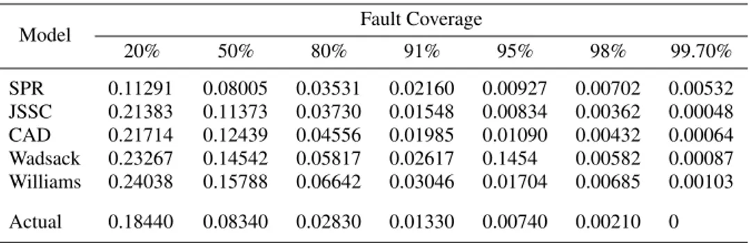
Over the past two decades a number of attempts have been made to quantify the effectiveness of test programs—that is, determine how many defective chips will be detected by the tester and how many will slip through the test process and reach the end user. Different researchers have come up with different equations for comput-ing defect level. The discrepancies are based on the fact that they start with differ-ent assumptions about fault distributions. Some of it is a result of basing results on different technologies, and some of it is a result of working with processes that have different quality levels, different failure mechanisms, and/or different defect distributions. We present here a survey of some of the equations that have been derived over the years to compute defect level as a function of process yields and test coverage.
In 1978 Wadsack16 derived the following equation:
yr = (1 − f)⋅(1 − y) (1.13)
where yr denotes the field reject rate—that is, the fraction of defective chips that passed the test and were shipped to the customer. The variable y, 0 ≤ y ≤ 1, denotes the actual yield of the process, and f, 0 ≤ f ≤ 1, denotes the fault coverage. In 1981 Williams and Brown developed the following equation:
DL = 1 − Y(1− T) (1.14)
In this equation the field reject rate is DL (defect level), the variable Y represents the yield of the manufacturing process, and the variable T represents the test percentage where, as in Eq. (1.13), each of these is a fraction between 0 and 1.
Example If it were possible to test for all defects, then
On the other hand, if no defective units were manufactured, then y = 1 and yr = (1 − f)⋅(1 − 1) = 0 from Eq. (1.13) Y = 1 and DL = 1 − 1(1−T) = 0 from Eq. (1.14)
In either situation, no defective units are shipped, regardless of which equation is
used.
For either of these equations, if the yield is known, it is possible to find the fault coverage required to achieve a desired defect level. Using Eq. (1.14), the test frac-tion T is
(1.15)
Example Integrated circuits (ICs) are manufactured on wafers—round, thin silicon substrates. After processing, individual ICs are tested. The wafer is diced and the die that tested bad are discarded. If the yield of good die is 60%, and we want a defect level not to exceed 0.1%, what level of testing must we achieve? Using Eq. (1.15), we get
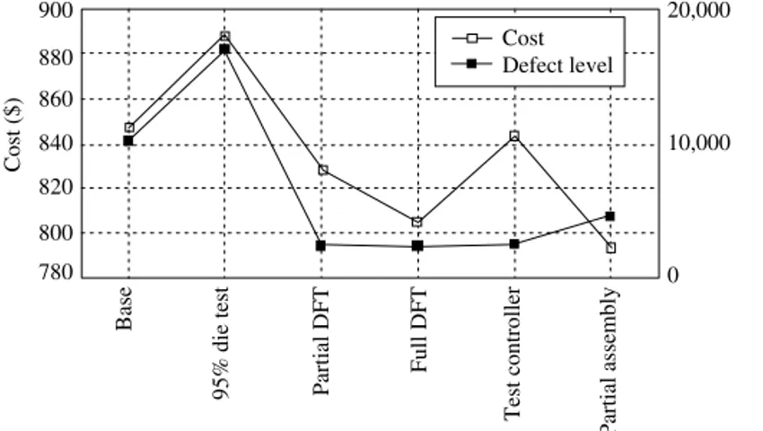
This equation is pessimistic for VLSI. In later paragraphs we will look at other equations that, based on clustering of faults, give more favorable results. Neverthe-less, this equation illustrates an important concept. Test cost is not a linear function. Experience indicates that test cost follows the curve illustrated in Figure 1.4.
This curve tells us that we reach a point where substantial expenditures provide only marginal improvement in testability. At some point, additional gains become exorbitantly expensive and may negate any hope for profitability of the product. However, looking again at Eq. (1.14), we see that the defect level is a function of both testability and yield. Therefore, we may be able to achieve a desired defect level by improving yield.
Figure 1.4 Typical cost curve for testing.
T 1 log(1–DL)
Y ( )
log
---– =
T 1 log(1–0.001) 0.6
( )
log
---– 1–0.001956 0.9980
= = =
Cost
Percent tested
100%
MEASURING TEST EFFECTIVENESS 17
Example Yield is improved to Y = 70%; what percentage of testing must be achieved to hold DL below 0.1%?
Equations (1.13) and (1.14) give the same results at the endpoints, but slightly different results between the endpoints. To understand why, it is necessary to look at the assumptions behind the derivations. Wadsack assumes that yi = (1 − y)i, where yi represents the chips with i faults and y represents the actual functional yield. Williams and Brown assume the existence of n faults, that all faults have equal prob-ability Pn of occurrence, and that the number of chips with i faults is
Working out the derivations from these different starting points results in the differ-ent equations. However, regardless of which equation is used, the key point is that, in order to achieve an acceptable quality level AQL (= 1 − DL), the fault coverage has to be nearly perfect. In the words of Williams and Brown, the equations are intended to “give estimates for quick calculations.” Wadsack, in his paper, points out that even in a circuit with 100% fault coverage, a failure occurred on the tester after the point where the test program had achieved 100% coverage of the faults. But then he points out that, in general, his derivation tends to be pessimistic.
Other authors have found the equations to be pessimistic; that is, even with fault coverage significantly less than that required by the equations, the quality level is better than predicted by the equations. For instance, Wiscombe17 states that the Williams–Brown model “predicts higher defect levels than seen in practice.” Max-well et al. point out that for a defect level of less than 0.1%, the Williams–Brown equation required fault coverage in excess of 99.6%. However, they were able to realize those defect levels with about 96% fault coverage.18
The question of fault coverage versus defect levels was studied by Agrawal et al. in 1982.19 Their study was motivated by the observation that the defect level equa-tions “produced satisfactory results for chips with high yield (typically, SSI and MSI), but the predictions were too pessimistic for larger chips with lower yield.” The authors hypothesize the existence of n faults for a faulty chip, and then examine the consequences of that assumption. They derive the following equation:
(1.16)
In this equation, y is the yield, n0 is the average number of faults on a faulty chip, f is the fault coverage, and r(f) is the field reject rate for f. If the fault coverage is held fixed, then the defect level goes down as n0 increases. The papers cited here suggest that the value n0 = 3 appears to give reasonably good results at predicting defect level. The model that was used to develop Eq. (1.16), referred to as the JSCC model, was subsequently refined using what the authors called the CAD model.20 A Poisson